• Acta Optica Sinica
  • Vol. 39, Issue 11, 1124002 (2019)
Ruxue Wei1、3, Yanwei Wang2、4, Liwen Jiang1, Xuqing Sun1, Hongyao Liu1, Chang Wang1、3, Xinchao Lu1、*, Weier Lu2、5、6、**, Yang Xia2、5、6, and Chengjun Huang1
Author Affiliations
  • 1Health Electronics Center, Institute of Microelectronics, Chinese Academy of Sciences, Beijing 100029, China
  • 2Microelectronic Instrument and Equipment Center, Institute of Microelectronics, Chinese Academy of Sciences, Beijing 100029, China
  • 3University of Chinese Academy of Sciences, Beijing 100049, China
  • 4Beijing Jiaotong University, Beijing 100044, China
  • 5Beijing Research Center of Engineering and Technology of Instrument and Equipment for Microelectronics Fabrication, Beijing 100029, China
  • 6Beijing Key Laboratory of Integrated Circuit Test Technology, Beijing 100088, China
  • show less
    DOI: 10.3788/AOS201939.1124002 Cite this Article Set citation alerts
    Ruxue Wei, Yanwei Wang, Liwen Jiang, Xuqing Sun, Hongyao Liu, Chang Wang, Xinchao Lu, Weier Lu, Yang Xia, Chengjun Huang. Detection of Chemical Vapor Deposition-Prepared Graphene by Surface Plasmon Polariton Imaging[J]. Acta Optica Sinica, 2019, 39(11): 1124002 Copy Citation Text show less
    Surface detection of transferred graphene. (a) Dark-field microscopy; (b) SEM
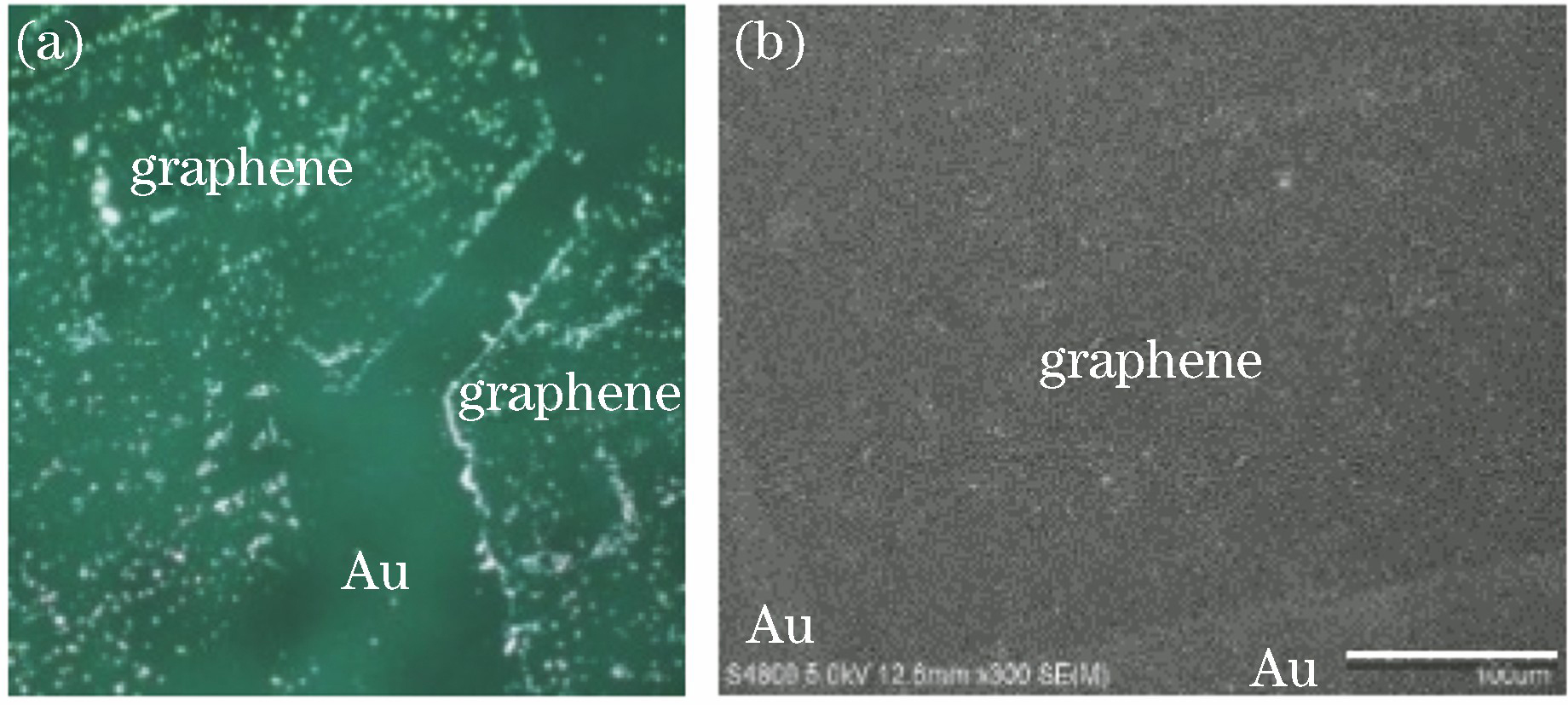
    Fig. 1. Surface detection of transferred graphene. (a) Dark-field microscopy; (b) SEM
    Schematic of optical path of SPP microscopic imaging
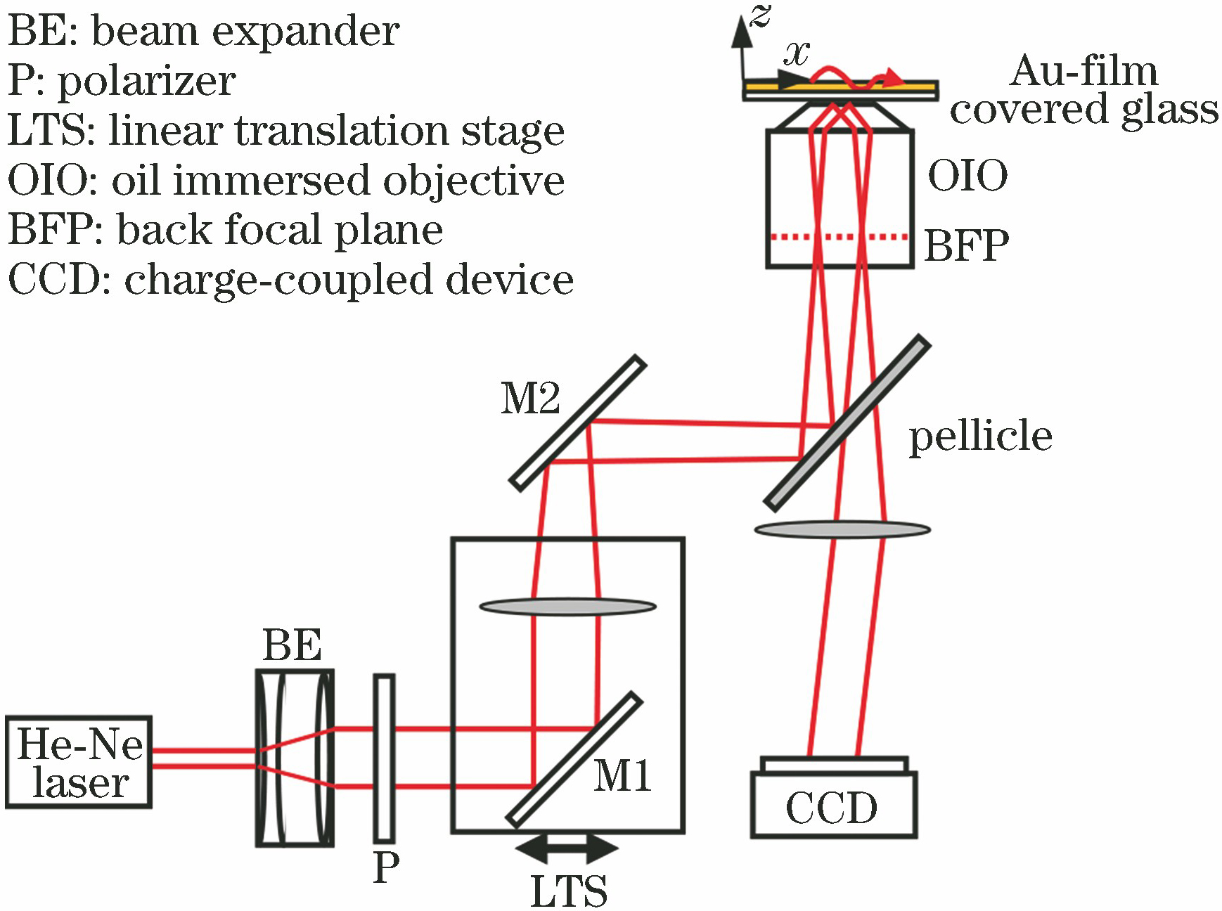
    Fig. 2. Schematic of optical path of SPP microscopic imaging
    Principle of graphene detection by SPP. (a) Schematic of SPP excited by Kretschmann configuration; (b) change of reflectance introduced by refractive index of graphene at interface; (c) change of SPP field distribution on interface induced by defects (dot: defect; straight line: incident SPP; dashed line: scattered SPP)
    Fig. 3. Principle of graphene detection by SPP. (a) Schematic of SPP excited by Kretschmann configuration; (b) change of reflectance introduced by refractive index of graphene at interface; (c) change of SPP field distribution on interface induced by defects (dot: defect; straight line: incident SPP; dashed line: scattered SPP)
    SPP imaging of different graphene edges and propagation direction of SPP is shown as arrow
    Fig. 4. SPP imaging of different graphene edges and propagation direction of SPP is shown as arrow
    Internal imaging of graphene and propagation direction of SPP is shown as arrow. (a) SPP imaging; (b) SEM imaging
    Fig. 5. Internal imaging of graphene and propagation direction of SPP is shown as arrow. (a) SPP imaging; (b) SEM imaging
    Imaging of wrinkles and break on edge of transferred graphene and propagation direction of SPP is shown as arrow. (a) SPP imaging; (b) SEM imaging
    Fig. 6. Imaging of wrinkles and break on edge of transferred graphene and propagation direction of SPP is shown as arrow. (a) SPP imaging; (b) SEM imaging
    Imaging of impurity nanoparticles on transferred graphene and propagation direction of SPP is shown as arrow. (a) SPP imaging; (b) SEM imaging
    Fig. 7. Imaging of impurity nanoparticles on transferred graphene and propagation direction of SPP is shown as arrow. (a) SPP imaging; (b) SEM imaging
    Imaging of other impurities on transferred graphene and propagation direction of SPP is shown as arrow. (a) SPP imaging; (b) SEM imaging
    Fig. 8. Imaging of other impurities on transferred graphene and propagation direction of SPP is shown as arrow. (a) SPP imaging; (b) SEM imaging
    Ruxue Wei, Yanwei Wang, Liwen Jiang, Xuqing Sun, Hongyao Liu, Chang Wang, Xinchao Lu, Weier Lu, Yang Xia, Chengjun Huang. Detection of Chemical Vapor Deposition-Prepared Graphene by Surface Plasmon Polariton Imaging[J]. Acta Optica Sinica, 2019, 39(11): 1124002
    Download Citation