• Journal of Semiconductors
  • Vol. 41, Issue 1, 011301 (2020)
Chao Zhao1、2、3、4, Bo Xu3、4, Zhijie Wang3、4, and Zhanguo Wang3、4
Author Affiliations
  • 1JARA-Fundamentals of Future Information Technology (JARA-FIT) and RWTH Aachen University, 52074 Aachen, Germany
  • 2Peter Grünberg Institute (PGI-9), Forschungszentrum Jülich, 52425 Jülich, Germany
  • 3Key Laboratory of Semiconductor Materials Science, Institute of Semiconductors, Chinese Academy of Sciences and Beijing Key Laboratory of Low Dimensional Semiconductor Materials and Devices, Beijing 100083, China
  • 4College of Materials Science and Opto-Electronic Technology, University of Chinese Academy of Sciences, Beijing 101804, China
  • show less
    DOI: 10.1088/1674-4926/41/1/011301 Cite this Article
    Chao Zhao, Bo Xu, Zhijie Wang, Zhanguo Wang. Boron-doped III–V semiconductors for Si-based optoelectronic devices[J]. Journal of Semiconductors, 2020, 41(1): 011301 Copy Citation Text show less
    (Color online) The bandgap energy versus lattice constant of the III–V semiconductor material system. Reproduced with permission from Ref. [10]. Copyright 2013, Miguel ángel Caro Bayo.
    Fig. 1. (Color online) The bandgap energy versus lattice constant of the III–V semiconductor material system. Reproduced with permission from Ref. [10]. Copyright 2013, Miguel ángel Caro Bayo.
    (Color online) (a) The number of publications and (b) times cited on BGaAs per year since 2000. Keyword: “BGaAs”. Web of Science search conducted: August 9, 2019.
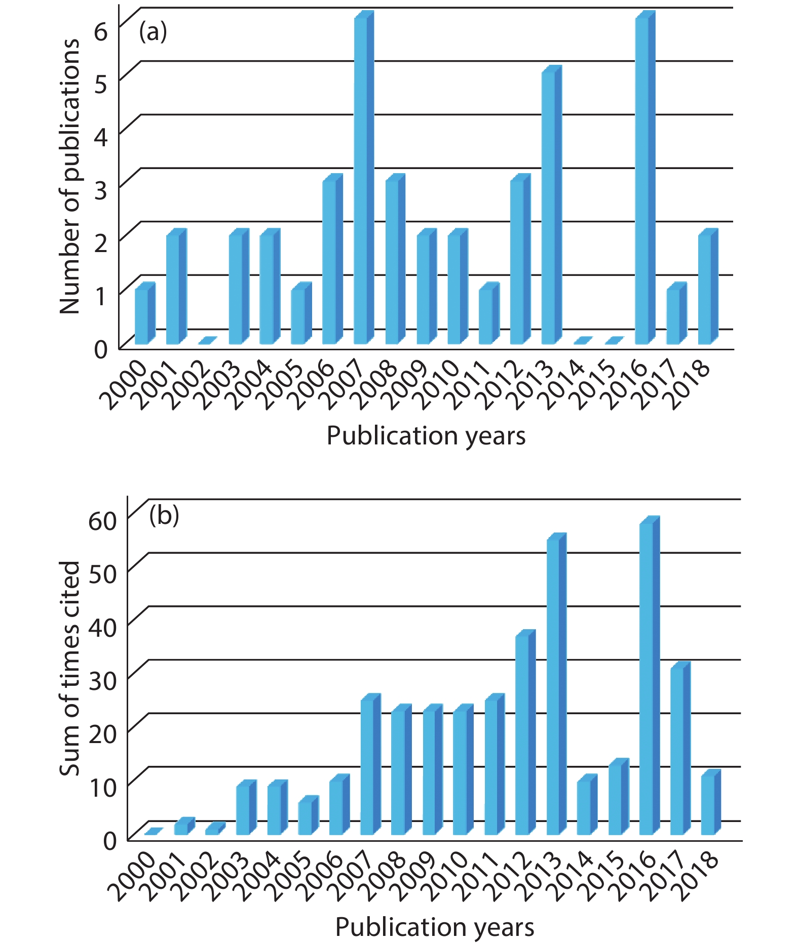
    Fig. 2. (Color online) (a) The number of publications and (b) times cited on BGaAs per year since 2000. Keyword: “BGaAs”. Web of Science search conducted: August 9, 2019.
    (Color online) Calculated bandgap versus lattice-constant for III–V compounds including B-doped alloy. Reproduced with permission from Ref. [26]. Copyright 2019, OSA Publishing.
    Fig. 3. (Color online) Calculated bandgap versus lattice-constant for III–V compounds including B-doped alloy. Reproduced with permission from Ref. [26]. Copyright 2019, OSA Publishing.
    Rocking curves of BGaAs and BxGa1–x–yInyAs. Reproduced with permission from Ref. [27]. Copyright 2000, AIP Publishing.
    Fig. 4. Rocking curves of BGaAs and BxGa1–xyInyAs. Reproduced with permission from Ref. [27]. Copyright 2000, AIP Publishing.
    (Color online) XRD rocking curves of the (004) peak for a GaAsBi ternary alloy and BGaAsBi alloy with different boron content. Reproduced with permission from Ref. [29]. Copyright 2012, Elsevier.
    Fig. 5. (Color online) XRD rocking curves of the (004) peak for a GaAsBi ternary alloy and BGaAsBi alloy with different boron content. Reproduced with permission from Ref. [29]. Copyright 2012, Elsevier.
    (Color online) (a) Apparent boron concentration and (b) surface roughness versus Bi flux for samples. Reproduced with permission from Ref. [30]. Copyright 2012, Elsevier.
    Fig. 6. (Color online) (a) Apparent boron concentration and (b) surface roughness versus Bi flux for samples. Reproduced with permission from Ref. [30]. Copyright 2012, Elsevier.
    AFM images of the surface with increasing boron content. Reproduced with permission from Refs. [17, 22]. Copyright 2003, AIP Publishing.
    Fig. 7. AFM images of the surface with increasing boron content. Reproduced with permission from Refs. [17, 22]. Copyright 2003, AIP Publishing.
    (a) Temperature dependence of PL peak energy of BGaAs epilayers. Reproduced with permission from Ref. [36]. Copyright 2010, Elsevier. (b) Low-temperature PL spectra of BInGaAs epilayer and quantum well. Reproduced with permission from Ref. [39]. Copyright 2012, Elsevier.
    Fig. 8. (a) Temperature dependence of PL peak energy of BGaAs epilayers. Reproduced with permission from Ref. [36]. Copyright 2010, Elsevier. (b) Low-temperature PL spectra of BInGaAs epilayer and quantum well. Reproduced with permission from Ref. [39]. Copyright 2012, Elsevier.
    (Color online) Schematic of spatial potential fluctuation and possible paths of carrier movement. Reproduced with permission from Ref. [41]. Copyright 2016, Elsevier.
    Fig. 9. (Color online) Schematic of spatial potential fluctuation and possible paths of carrier movement. Reproduced with permission from Ref. [41]. Copyright 2016, Elsevier.
    AFM images of 200 nm BGaAs/GaAs epilayers with various diborane flow-rates. Reproduced with permission from Ref. [44]. Copyright 2008, Elsevier.
    Fig. 10. AFM images of 200 nm BGaAs/GaAs epilayers with various diborane flow-rates. Reproduced with permission from Ref. [44]. Copyright 2008, Elsevier.
    Boron composition of BGaAs as a function of boron concentration in the gas phase. Reproduced with permission from Ref. [50]. Copyright 2008, Elsevier.
    Fig. 11. Boron composition of BGaAs as a function of boron concentration in the gas phase. Reproduced with permission from Ref. [50]. Copyright 2008, Elsevier.
    Cross-sectional TEM images of (a) InGaAs/GaAs and (b) BInGaAs/GaAs. Reproduced with permission from Ref. [24]. Copyright 2013, AIP Publishing.
    Fig. 12. Cross-sectional TEM images of (a) InGaAs/GaAs and (b) BInGaAs/GaAs. Reproduced with permission from Ref. [24]. Copyright 2013, AIP Publishing.
    (a) X-ray rocking curve of a BGaAs ternary. (b) Boron composition as a function of substrate temperature. Reproduced with permission from Ref. [54]. Copyright 2004, Elsevier.
    Fig. 13. (a) X-ray rocking curve of a BGaAs ternary. (b) Boron composition as a function of substrate temperature. Reproduced with permission from Ref. [54]. Copyright 2004, Elsevier.
    (Color online) AFM images for BGaAs grown at different conditions. Reproduced with permission from Ref. [50]. Copyright 2017, Elsevier.
    Fig. 14. (Color online) AFM images for BGaAs grown at different conditions. Reproduced with permission from Ref. [50]. Copyright 2017, Elsevier.
    (Color online) (a) I–V measurements on nanowires with and without boron; (b) TEM image of nanowires. Reproduced with permission from Ref. [50]. Copyright 2019, John Wiley and Sons.
    Fig. 15. (Color online) (a) I–V measurements on nanowires with and without boron; (b) TEM image of nanowires. Reproduced with permission from Ref. [50]. Copyright 2019, John Wiley and Sons.
    (Color online) (a) ω–2θ scans of BGaAs films grown on a GaP buffer. (b) Reciprocal space mapping (RSM) of BGaAs layers grown on a GaP buffer. Reproduced with permission from Ref. [50]. Copyright 2018, IEEE.
    Fig. 16. (Color online) (a) ω–2θ scans of BGaAs films grown on a GaP buffer. (b) Reciprocal space mapping (RSM) of BGaAs layers grown on a GaP buffer. Reproduced with permission from Ref. [50]. Copyright 2018, IEEE.
    (Color online) XRD of BGaAs films grown on GaAs substrates. Reproduced with permission from Ref. [26]. Copyright 2019, OSA Publishing.
    Fig. 17. (Color online) XRD of BGaAs films grown on GaAs substrates. Reproduced with permission from Ref. [26]. Copyright 2019, OSA Publishing.
    (Color online) Room temperature photoluminescence of BGaAs and BGaInAs alloy. Reproduced with permission from Ref. [26]. Copyright 2019, OSA Publishing.
    Fig. 18. (Color online) Room temperature photoluminescence of BGaAs and BGaInAs alloy. Reproduced with permission from Ref. [26]. Copyright 2019, OSA Publishing.
    Comparison of the boron concentration in GaP and GaAs. Reproduced with permission Ref. [50]. Copyright 2013, Elsevier.
    Fig. 19. Comparison of the boron concentration in GaP and GaAs. Reproduced with permission Ref. [50]. Copyright 2013, Elsevier.
    A comparison of calculated mixing enthalpies for GaAs1−xNx and BxGa1−xAs. Reproduced with permission from Ref. [59]. Copyright 2000, AIP Publishing.
    Fig. 20. A comparison of calculated mixing enthalpies for GaAs1−xNx and BxGa1−xAs. Reproduced with permission from Ref. [59]. Copyright 2000, AIP Publishing.
    SystembVDbCEbSRbtotbthebexp
    Mixed cation
    BAlN4.881.62–1.055.45
    BGaN7.471.47–1.667.284.3 (x = 0.6)
    BInN14.732.03–3.2913.48
    BAlP4.411.20–0.954.65
    BGaP4.611.04–1.004.65
    BInP8.741.61–1.928.43
    BAlAs2.771.17–0.593.35
    BGaAs3.031.02–0.663.393.5 (x < 0.6) 2.3 (x < 0.4)
    BInAs6.081.58–1.346.32
    BAlSb0.151.07–0.031.18
    BGaSb–0.170.92–0.090.65
    BInSb0.701.48–0.082.10
    Mixed anion
    BNP2.101.943.897.949.92
    BNAs5.132.294.8712.309.33
    BNSb14.303.521.9619.7810.27, 21.19
    BPSb4.480.561.766.800.038
    BPAs0.520.340.000.87–0.06
    BAsSb1.940.471.103.500.10
    Table 1. Calculated bowing btot as well as its three contributions in eV. Reproduced with permission from Ref. [23]. Copyright 2007, Elsevier.
    Chao Zhao, Bo Xu, Zhijie Wang, Zhanguo Wang. Boron-doped III–V semiconductors for Si-based optoelectronic devices[J]. Journal of Semiconductors, 2020, 41(1): 011301
    Download Citation