
Chao Zhao, Bo Xu, Zhijie Wang, Zhanguo Wang. Boron-doped III–V semiconductors for Si-based optoelectronic devices[J]. Journal of Semiconductors, 2020, 41(1): 011301
- Journal of Semiconductors
- Vol. 41, Issue 1, 011301 (2020)
Abstract
1. Introduction
Silicon-based optoelectronic devices offer a solution for the increasing demand for high speed and high amount of data transmission. However, the bottleneck for the development turns out to be the lack of suitable light source on silicon due to the indirect bandgap of the material. In the meantime, group III–V semiconductor-based light sources are mature. Different light-emitting diodes and lasers have been realized by either GaAs or GaN[
Compared to their antecessor Si, III–V compound semiconductors have versatile properties such as direct bandgap, higher carrier mobility, and smaller electron effective mass, making them highly attractive for microelectronic and optoelectronic applications in solid-state lighting, wireless communication, artificial intelligence, high-speed train, clean energy generation, and radar systems[
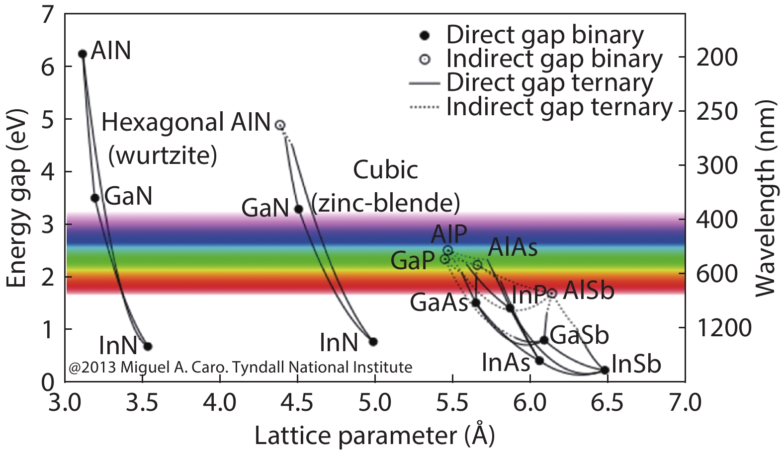
![]()
Figure 1.(Color online) The bandgap energy versus lattice constant of the III–V semiconductor material system. Reproduced with permission from Ref. [
The natural solution is to integrate III–V lasers on Si substrates by heterogeneous or monolithic ways. In heterogeneous integration, the III–V laser is wafer bonded to a Si substrate. The heat dissipation problem may deteriorate the device performance. John Bower et al. from the University of California, Santa Barbara demonstrated the on-chip and inter-chip optical interconnects using light-emitting devices bonded onto silicon substrates[
Besides light emitters, a photodetector, especially in the infrared range on Si, will enable widespread applications on military action, artificial intelligence, and so on. A wafer-scale fabrication process will lead to the large-area photodetector, which also makes it affordable. Although silicon itself is an efficient photodetector, it can only cover up to ~1.1 μm. III–V materials grown by metamorphic approaches lead to excessive dark currents. Therefore, a lattice-matching way of growing III–V materials on Si is needed.
In the early days, boron was introduced to remove the defect states in AlGaAs. In 1992, B-doped (Al, Ga)As was investigated by Tischler from IBM T. J. Watson Research Center to study the possibility to eliminate the DX centers in (Al, Ga)As[
Furthermore, the BGaInAs alloy was found can be tuned to be lattice-matched to GaAs and Si with a bandgap smaller than GaAs[
Because of the problems in the epitaxy such as B surface segregation, deteriorated surface, and B antisite formation, the research on B-doped III–V semiconductors is sparse[
![]()
Figure 2.(Color online) (a) The number of publications and (b) times cited on BGaAs per year since 2000. Keyword: “BGaAs”. Web of Science search conducted: August 9, 2019.
Until now, we lack a useful review that appropriately summarizes the development, problems, and current situation of these boron-doped III–V semiconductors, along with their various applications. In this review, we focus on the epitaxy of BGaAs semiconductors and discuss the broad potential optoelectronic applications, including light emitters and photodetectors. The growth mechanisms, growth techniques, including metal-organic chemical vapor deposition (MOCVD) and molecular-beam epitaxy (MBE), and the optical properties of BGaAs are summarized in Section 2. In Section 3, we discuss different BGaAs compounds, investigating their characteristics and applications, followed by an elaboration on challenges and problems of boron-doped III–V semiconductors in Section 4. Finally, we give a summary and future perspectives of these materials in Section 5.
2. Properties and growth techniques of boron-doped III–V semiconductors
Since boron has highly different properties than other III and V elements, it is expected its incorporation into III–V semiconductors will induce a huge change in the properties of III–V semiconductors[
Because of the lattice constant, BGaAs has been suggested as a strain-compensation barrier in InGaAs(N) system. Although there are still arguments on the bandgap variation of BGaAs with boron composition, it is clear it can be a replacement for InGaAs(N) in the infrared wavelength range when adding indium to the compounds[
![]()
Figure 3.(Color online) Calculated bandgap versus lattice-constant for III–V compounds including B-doped alloy. Reproduced with permission from Ref. [
2.1. MOCVD
Similar to GaAs, BGaAs has been grown both by MOCVD and MBE. In the initial work, B-doped (Al, Ga)As was grown in a low-pressure metalorganic vapor phase epitaxy (MOVPE) system. In these systems, trimethylgallium (TMGa), trimethylaluminum (TMAl), and arsine (AsH3) were used as precursors for Ga, Al, and As. Diborane (B2H6) and trimethyl boron have been used as boron precursors[
2.2. MBE
BGaAs was first grown by Hoke from Raytheon Research Division using MBE in 1993[
3. Boron-doped III–V semiconductors: materials and devices
In this part, we will review the development and research progress of boron-doped III–V semiconductors from various groups. Since most groups reported the growth using MOCVD, we will introduce the progress in this field, then also cover MBE related growth and a few theoretical works.
The early study mainly focused on the growth conditions optimization and characterization of B(In)GaAs layers on GaAs substrates. In 2000, Geisz et al. from National Renewable Energy Laboratory reported the growth of BGaInAs alloys with boron concentration up to 4%, which has a lattice matched to GaAs[
![]()
Figure 4.Rocking curves of BGaAs and B
To further improve the boron incorporation, the precursors used in MOCVD were studied systematically. In 2001, they first analyzed the boron incorporation into BxGa1–xAs using different Ga precursors (TEG and TMG) in MOCVD, although they behave differently, the incorporation efficiency and maximum achievable boron concentration both decrease when growth temperatures are higher than 600 °C[
Bi has been used as a conventional surfactant in other material systems. To further improve the growth, the lab studied the growth of quaternary BGaAsBi lattice-matched to GaAs substrates in 2012[
![]()
Figure 5.(Color online) XRD rocking curves of the (004) peak for a GaAsBi ternary alloy and BGaAsBi alloy with different boron content. Reproduced with permission from Ref. [
Similar to other reports, the amount of substitutional boron decreases with increasing substrate temperatures. However, the addition of a bismuth surfactant appears to force boron onto substitutional sites (see Fig. 6(a)), and makes the epilayers smoother (see Fig. 6(b))[
![]()
Figure 6.(Color online) (a) Apparent boron concentration and (b) surface roughness versus Bi flux for samples. Reproduced with permission from Ref. [
In 2003, H. Dumont from Université Claude Bernard Lyon 1 studied the growth of BGaAs on GaAs substrates[
![]()
Figure 7.AFM images of the surface with increasing boron content. Reproduced with permission from Refs. [
Besides surface morphology, the group also studied the optical properties of these BGaAs epilayers in 2004, which is necessary for their applications in optoelectronic devices. The temperature-dependent photoluminescence peak position showed an S-shaped behavior, which is a sign of the localized states due to nonuniform doping of boron atoms within the BGaAs epilayer. Similar behavior is also common in InGaAs layers grown on GaAs where indium segregation is observed. This is also verified by the large broadening of the BGaAs PL peak[
![]()
Figure 8.(a) Temperature dependence of PL peak energy of BGaAs epilayers. Reproduced with permission from Ref. [
The group also investigated the BInGaAs single quantum well (SQW) grown by MOVPE[
Furthermore, BInGaAs/GaAs quantum well with high indium composition was studied, it shows that a BInGaAs can be grown lattice-matched to GaAs as predicted. The temperature dependence of the PL peak energy showed an S-shaped behavior as a result of the competition process between localized and delocalized states of boron clusters. A model of carrier dynamics model was developed, as shown in Fig. 9. It explains the potential fluctuation caused by clusters, localized states, and possible paths for carrier transport and recombination in the material when the temperature increases[
![]()
Figure 9.(Color online) Schematic of spatial potential fluctuation and possible paths of carrier movement. Reproduced with permission from Ref. [
Besides, the group also studied the influence of boron surface enrichment on the growth of BGaAs by MOVPE[
![]()
Figure 10.AFM images of 200 nm BGaAs/GaAs epilayers with various diborane flow-rates. Reproduced with permission from Ref. [
Besides the AFM, PL characterization, photo-thermal deflection (PTD) technique was adopted to study the nonradiative recombination process in BGaAs/GaAs alloy in 2013. It was found with the increase of the boron composition, the induced localized states, clusters at BGaAs/GaAs interface, and roughness and imperfection of the surface change the transport properties of the BGaAs epilayer. Moreover, the thermal conductivity of BGaAs layers was found to decrease due to the allowing effects[
In 2008, Xiaomin Ren’s group from Beijing University of Posts and Telecommunications studied the growth of BGaAs on GaAs using LP-MOCVD[
![]()
Figure 11.Boron composition of BGaAs as a function of boron concentration in the gas phase. Reproduced with permission from Ref. [
In 2013, the group further studied the effect of boron incorporation on the InGaAs/GaAs MQWs[
![]()
Figure 12.Cross-sectional TEM images of (a) InGaAs/GaAs and (b) BInGaAs/GaAs. Reproduced with permission from Ref. [
Compared to MOCVD, the study on BGaAs grown by MBE is relatively less. Gupta et al. from the University of Rochester reported BGaAs single crystal layer with boron composition up to 0.25% grown by MBE in 2000[
In 2004, Groenert from Infineon Technologies AG in Germany studied the growth of BGaAs by MBE, where the boron was provided by a high-temperature effusion cell. It was found that by reducing the growth temperature below 540 °C and increasing the V/III ratio above 20 it would improve the boron incorporation in the epitaxial layers; in the meantime, high temperature and low V/III ratio would lead to the B incorporation on interstitial lattice sites. The peak splitting in Fig. 13(a) was used to calculate the boron composition. As shown in the discrepancy of the boron composition at high temperature in Fig. 13(b), a large fraction of B atoms were not on Ga lattice sites at high temperatures. Because of the slow boron surface migration on GaAs and high cohesive energy of binary BAs compared to GaAs[
![]()
Figure 13.(a) X-ray rocking curve of a BGaAs ternary. (b) Boron composition as a function of substrate temperature. Reproduced with permission from Ref. [
In 2017, Detz et al. from TU Wien studied the boron incorporation depending on the growth rate of GaAs. In their system, a pyrolytic graphite crucible operating at 1725–1800 °C was used for the boron source. It was found that a higher GaAs growth rate leads to a higher BAs growth rate[
![]()
Figure 14.(Color online) AFM images for BGaAs grown at different conditions. Reproduced with permission from Ref. [
In 2019, Lancaster et al. from TU Wien also studied BGaAs but in the nanowire form. It was found that the surface segregation led to the high boron concentration at the edge. Its incorporation on antisites explains its p-type behavior[
![]()
Figure 15.(Color online) (a)
In 2018, Bank from the University of Texas at Austin reported exciting progress in this field. The growth of BGaAs on GaP using their high kinetically-limited growth regime with a high growth rate, a low substrate temperature, and using bismuth as a surfactant to limit surface diffusion of boron and showed promoted boron substitutional incorporation. The further increase of boron for lattice-matching BGaAs to GaP leads to the XRD peaks broadening and absence of fringes due to the phase segregation, as shown in Fig. 16. This happened because of the lack of a P-terminated surface during deoxidation and a GaP buffer layer to screen defects from the substrates[
![]()
Figure 16.(Color online) (a)
In 2019, Bank’s group further demonstrated 1.31 μm room temperature emission of BGaInAs alloy on GaAs substrates[
![]()
Figure 17.(Color online) XRD of BGaAs films grown on GaAs substrates. Reproduced with permission from Ref. [
To further extend the emission wavelength, indium was added into BGaAs alloy. Although BGaAs is a poor emitter due to the boron cluster states. The incorporation of indium atoms lowers the conduction band edge down to boron cluster states[
![]()
Figure 18.(Color online) Room temperature photoluminescence of BGaAs and BGaInAs alloy. Reproduced with permission from Ref. [
In comparison to boron-doped arsenides, Sommer et al. from Philipps-Universitat investigated the phosphorus-based materials doped with boron. The quaternary system (BGa)(AsP) was also discussed in their report[
![]()
Figure 19.Comparison of the boron concentration in GaP and GaAs. Reproduced with permission Ref. [
Besides experimental work, few theoretical works have been reported to predict and study the properties of these materials. The National Renewable Energy Laboratory also studied the electronic structure of boron-doped III–V semiconductor alloys[
![]()
Figure 20.A comparison of calculated mixing enthalpies for GaAs1−
Zaoui from Université des Sciences et de la Technologie de Lille studied the bandgap bowing of boron-doped III–V semiconductors[
In 2007, Jenichen et al. from Leibniz-Institute for Surface Modification in Germany studied the stabilities and band gaps of B-doped III–V semiconductors using density-functional supercell calculations by considering the arrangement and composition of (B, In) atoms. It was found that in the case of boron antisite instead of isovalent substitution, the bandgap would strongly reduce[
4. Challenges and problems
Until now, different groups have reported the growth of boron-doped III–V semiconductors by MBE or MOCVD; the properties of the materials were also predicted by different theoretical groups. However, there are still many challenges to their development and applications. First, although researchers tried to improve the boron composition doped in these materials, it only reaches 12% on GaAs and 15.5% on GaP recently. A new growth regime is needed to increase the boron composition further and extend the wavelength range of BInGaAs, and make it more practical for infrared applications. Second, the bandgap theory and growth mechanism are still not clear; researchers reported contradictory results on these materials. Moreover, most of the works still focus on material characterization; the material quality is still not at a level ready for different optoelectronic devices. Until now, only very few device results from this material system was reported.
5. Summary and perspectives
To summarize, we have reviewed the development of boron-doped III–V semiconductors, including different growth techniques such as MBE and MOCVD, the growth mechanism and their characterization, and few applications in optoelectronic devices. Although the first study was reported more than two decades ago, the materials remain undeveloped. To provide a better understanding of this field, we have detailed the progress from various groups, not only those who study the growth of materials but also who predict material properties theoretically, not only by MOCVD but also by MBE. We have further focused on their recent applications in optoelectronic devices such as lasers and detectors. However, it is necessary to further understand the boron doping behavior and extend the device application of boron-doped materials.
With further development in boron-doped III–V semiconductors, they will find practical applications in laser and detectors in the near- and mid-infrared range, not only on III–V substrates but also on large-scale, low-cost Si substrates. These devices will be essential for an optoelectronic integrated circuit. Moving forward, there is enormous potential for employing boron-doped III–V semiconductors in cross-disciplinary applications, such as autonomous vehicles, biomedical instrumentation, and tactical intelligence.
References
[1] B Janjua, T K Ng, C Zhao et al. True yellow light-emitting diodes as phosphor for tunable color-rendering index laser-based white light. ACS Photonics, 3, 2089(2016).
[2] C Zhao, T K Ng, C C Tseng et al. InGaN/GaN nanowires epitaxy on large-area MoS2 for high-performance light-emitters. RSC Adv, 7, 26665(2017).
[3] C Zhao, M Ebaid, H Zhang et al. Quantified hole concentration in AlGaN nanowires for high-performance ultraviolet emitters. Nanoscale, 10, 15980(2018).
[4] C Zhao, N Alfaraj, R C Subedi et al. III-nitride nanowires on unconventional substrates: From materials to optoelectronic device applications. Prog Quantum Electron, 61, 1(2018).
[5] B Janjua, H Sun, C Zhao et al. Self-planarized quantum-disks-in-nanowires ultraviolet-B emitters utilizing pendeo-epitaxy. Nanoscale, 9, 7805(2017).
[6] M Ebaid, D Priante, G Liu et al. Unbiased photocatalytic hydrogen generation from pure water on stable Ir-treated In0.33Ga0.67N nanorods. Nano Energy, 37, 158(2017).
[7] C Zhao, Y H Chen, B Xu et al. Study of the wetting layer of InAs/GaAs nanorings grown by droplet epitaxy. Appl Phys Lett, 92, 063122(2008).
[8] C Zhao, Y H Chen, B Xu et al. Evolution of InAs nanostructures grown by droplet epitaxy. Appl Phys Lett, 91, 033112(2007).
[9] G Siddiqi, Z Pan, S Hu. III–V semiconductor photoelectrodes. Semiconductors and Semimetals, 81(2017).
[10]
[11] G Roelkens, L Liu, D Liang et al. III–V/silicon photonics for on-chip and intra-chip optical interconnects. Laser Photonics Rev, 4, 751(2010).
[12] S Chen, W Li, J Wu et al. Electrically pumped continuous-wave III–V quantum dot lasers on silicon. Nat Photonics, 10, 307(2016).
[13] M A Tischler, P M Mooney, B D Parker et al. Metalorganic vapor phase epitaxy and characterization of boron-doped (Al,Ga)As. J Appl Phys, 71, 984(1992).
[14] J F Geisz, D J Friedman, S Kurtz et al. Epitaxial growth of BGaAs and BGaInAs by MOCVD. J Cryst Growth, 225, 372(2001).
[15] G L W Hart, A Zunger. Electronic structure of BAs and boride III–V alloys. Phys Rev B, 62, 13522(2000).
[16] W E Hoke. Molecular-beam epitaxial growth of boron-doped GaAs films. J Vac Sci Technol B, 11, 902(1993).
[17] V K Gupta, M W Koch, N J Watkins et al. Molecular beam epitaxial growth of BGaAs ternary compounds. J Electron Mater, 29, 1387(2000).
[18] F Tian, B Song, X Chen et al. Unusual high thermal conductivity in boron arsenide bulk crystals. Science, 361, 582(2018).
[19] S Li, Q Zheng, Y Lv et al. High thermal conductivity in cubic boron arsenide crystals. Science, 361, 579(2018).
[20] J S Kang, M Li, H Wu et al. Experimental observation of high thermal conductivity in boron arsenide. Science, 361, 575(2018).
[21] H Detz, D MacFarland, T Zederbauer et al. Growth rate dependence of boron incorporation into B
[22] H Dumont, D Rutzinger, C Vincent et al. Surface segregation of boron in B
[23] S Azzi, A Zaoui, M Ferhat. On the importance of the band gap bowing in boron-based III–V ternary alloys. Solid State Commun, 144, 245(2007).
[24] D A Pryakhin. Growth of BGaAs layers on GaAs substrates by metal–organic vapor-phase epitaxy. Semiconductors, 39, 11(2005).
[25] H Dumont, J Dazord, Y Monteil et al. Growth and characterization of high quality B
[26] R H El-Jaroudi, K M McNicholas, B A Bouslog et al. Boron alloys for GaAs-based 1.3
[27] J F Geisz, D J Friedman, J M Olson et al. BGaInAs alloys lattice matched to GaAs. Appl Phys Lett, 76, 1443(2000).
[28] J F Geisz, D J Friedman, S Kurtz et al. Alternative boron precursors for BGaAs epitaxy. J Electron Mater, 30, 1387(2001).
[29] D A Beaton, A J Ptak, K Alberi et al. Quaternary bismide alloy lattice matched to GaAs. J Cryst Growth, 351, 37(2012).
[30] A J Ptak, D A Beaton, A Mascarenhas. Growth of BGaAs by molecular-beam epitaxy and the effects of a bismuth surfactant. J Cryst Growth, 351, 122(2012).
[31] H Dumont, Y Monteil. Some aspects on thermodynamic properties, phase diagram and alloy formation in the ternary system BAs–GaAs—Part II: BGaAs alloy formation. J Cryst Growth, 290, 419(2006).
[32] F Saidi, F Hassen, H Maaref et al. Optical study of B
[33] F Saidi, F Hassen, H Dumont et al. Comparative optical study of GaAs1−
[34] Q Wang, Z Jia, X Ren et al. Effect of boron incorporation on the structural and photoluminescence properties of highly-strained In
[35] R Hamila, F Saidi, A Fouzri et al. Clustering effects in optical properties of BGaAs/GaAs epilayers. J Lumin, 129, 1010(2009).
[36] R Hamila, F Saidi, P H Rodriguez et al. Growth temperature effects on boron incorporation and optical properties of BGaAs/GaAs grown by MOCVD. J Alloys Compnd, 506, 10(2010).
[37] F Saidi, R Hamila, H Maaref et al. Structural and optical study of B
[38] P Rodriguez, L Auvray, H Dumont et al. Growth and characterization of BGaAs and BInGaAs epilayers on GaAs by MOVPE. J Cryst Growth, 298, 81(2007).
[39] R Hamila, F Saidi, H Maaref et al. Photoluminescence properties and high resolution X-ray diffraction investigation of BInGaAs/GaAs grown by the metalorganic vapour phase epitaxy method. J Appl Phys, 112, 063109(2012).
[40] R Hamila, F Saidi, P Rodriguez et al. Structural and optical study of BInGaAs/GaAs quantum wells grown by MOVPE emitting above 1.1 eV. Microelectron Eng, 149, 5(2016).
[41] T Hidouri, F Saidi, H Maaref et al. Localized state exciton model investigation of B-content effect on optical properties of BGaAs/GaAs epilayers grown by MOCVD. Vacuum, 132, 10(2016).
[42] T Hidouri, F Saidi, H Maaref et al. LSE investigation of the thermal effect on band gap energy and thermodynamic parameters of BInGaAs/GaAs single quantum well. Opt Mater, 62, 267(2016).
[43] T Hidouri, F Saidi, H Maaref et al. Impact of photoluminescence temperature and growth parameter on the exciton localized in B
[44] P Rodriguez, L Auvray, A Favier et al. Influence of boron surface enrichment on the growth mode of BGaAs epilayers grown on GaAs by metalorganic vapour phase epitaxy. Thin Solid Films, 516, 8424(2008).
[45] S Ilahi, M Baira, F Saidi et al. Non-radiative recombination process in BGaAs/GaAs alloys: Two layer photothermal deflection model. J Alloys Compnd, 581, 358(2013).
[46] S Ilahi, F Saidi, R Hamila et al. Photothermal deflection spectroscopy PDS investigation of optical and thermal properties of BGaAs/GaAs alloys. Curr Appl Phys, 13, 610(2013).
[47] S Ilahi, F Saidi, R Hamila et al. Shift of the gap energy and thermal conductivity in BGaAs/GaAs alloys. Physica B, 421, 105(2013).
[48] Q Wang, X Ren, F Wang et al. LP-MOCVD growth of ternary B
[49] Q Wang, X Ren, H Huang et al. Growth of B
[50] S Lancaster, H Groiss, T Zederbauer et al. Suppression of axial growth by boron incorporation in GaAs nanowires grown by self-catalyzed molecular beam epitaxy. Nanotechnology, 30, 065602(2019).
[51] S K Brierley, H T Hendriks, W E Hoke et al. Observation of boron-related photoluminescence in GaAs layers grown by molecular beam epitaxy. Appl Phys Lett, 63, 812(1993).
[52] A Kley, P Ruggerone, M Scheffler. Novel diffusion mechanism on the GaAs (001) surface: the role of adatom-dimer interaction. Phys Rev Letters, 79, 5278(1997).
[53] B Paulus, P Fulde, H Stoll. Cohesive energies of cubic III-V semiconductors. Phys Rev B, 54, 2556(1996).
[54] M E Groenert, R Averbeck, W Hösler et al. Optimized growth of BGaAs by molecular beam epitaxy. J Cryst Growth, 264, 123(2004).
[55] S Lancaster, A M Andrews, M Stoeger-Pollach et al. Influence of boron antisite defects on the electrical properties of MBE-grown GaAs nanowires. Phys Status Solidi B, 256, 1800368(2019).
[56] S R Bank, K M McNicholas, R H El-Jaroudi et al. Improved MWIR LED arrays on Si substrates for scene projectors. IEEE Research and Applications of Photonics In Defense Conference (RAPID)(2018).
[57] A Lindsay, E P O’Reilly. Theory of electronic structure of BGaAs and related alloys. Phys Status Solidi C, 5, 454(2008).
[58] N Sommer, R Buss, J Ohlmann et al. Growth of (BGa)As, (BGa)P, (BGa)(AsP) and (BGaIn)P by MOVPE. J Cryst Growth, 370, 191(2013).
[59] S B Zhang, A Zunger. Surface-reconstruction-enhanced solubility of N, P, As, and Sb in III–V semiconductors. Appl Phys Lett, 71, 677(1997).
[60] A Jenichen, C Engler. Stability and band gaps of InGaAs, BGaAs, and BInGaAs alloys: Density-functional supercell calculations. Phys Status Solidi B, 244, 1957(2007).
[61] A Jenichen, C Engler. Boron and indium substitution in GaAs (001) surfaces: Density-functional supercell calculations of the surface stability. Surf Sci, 601, 900(2007).
[62] A Jenichen, C Engler. Metalorganic chemical-vapour-deposition (MOCVD) of InGaAs, BGaAs, and BInGaAs: Quantum chemical calculations on the mechanisms. J Cryst Growth, 304, 26(2007).

Set citation alerts for the article
Please enter your email address
© Copyright 2018-2021 | Chinese Laser Press. All Rights Reserved 沪ICP备15018463号-20