• Photonics Research
  • Vol. 5, Issue 2, 113 (2017)
Yong-Pan Gao1, Tie-Jun Wang1, Cong Cao2, and Chuan Wang1、*
Author Affiliations
  • 1State Key Laboratory of Information Photonics and Optical Communications and School of Science, Beijing University of Posts and Telecommunications, Beijing 100876, China
  • 2School of Ethnic Minority Education, Beijing University of Posts and Telecommunications, Beijing 100876, China
  • show less
    DOI: 10.1364/PRJ.5.000113 Cite this Article Set citation alerts
    Yong-Pan Gao, Tie-Jun Wang, Cong Cao, Chuan Wang. Gap induced mode evolution under the asymmetric structure in a plasmonic resonator system[J]. Photonics Research, 2017, 5(2): 113 Copy Citation Text show less
    MIM structure studied in this paper. The waveguide and ring resonator have a width of 50 nm, the nearest distance between the two subjects is 10 nm, and the nanogap in the ring resonator is 2 nm. For convenience, here we give two points A and B to discuss later. The metal in this paper is Ag. Its Drude parameter is high frequency relative permittivity ε∞=3.7, the plasma frequency is ωp=9.1 eV, and the plasma decay is γp=0.018 eV.
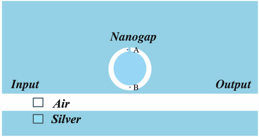
    Fig. 1. MIM structure studied in this paper. The waveguide and ring resonator have a width of 50 nm, the nearest distance between the two subjects is 10 nm, and the nanogap in the ring resonator is 2 nm. For convenience, here we give two points A and B to discuss later. The metal in this paper is Ag. Its Drude parameter is high frequency relative permittivity ε=3.7, the plasma frequency is ωp=9.1  eV, and the plasma decay is γp=0.018  eV.
    Electric field distribution of the input field with wavelength (a) 982 and (b) 1081 nm. Here we take the gap as the origin point and rotate around the ring resonator CCW with an angle of 2π. The inset figure shows the field magnitude of the electric field.
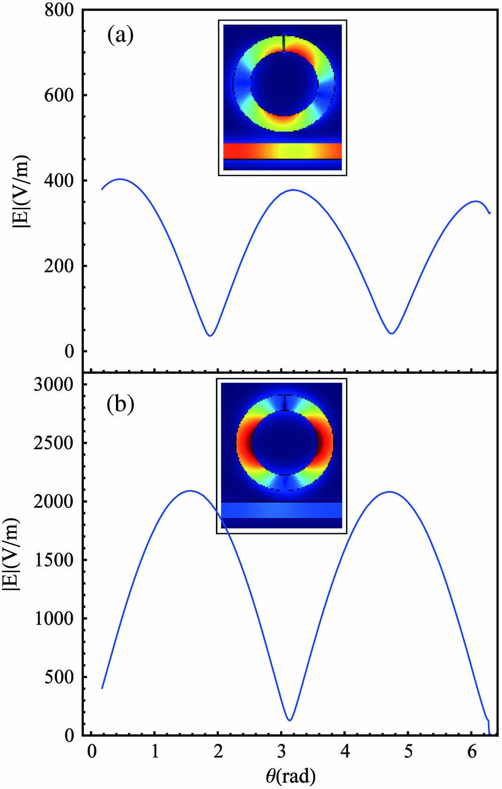
    Fig. 2. Electric field distribution of the input field with wavelength (a) 982 and (b) 1081 nm. Here we take the gap as the origin point and rotate around the ring resonator CCW with an angle of 2π. The inset figure shows the field magnitude of the electric field.
    Electric field distribution of the ring resonator in Fig. 1. The resonance wavelengths are (a) 982 and (b) 1081 nm. Here the gap is rotated CCW around the ring resonator from point B.
    Fig. 3. Electric field distribution of the ring resonator in Fig. 1. The resonance wavelengths are (a) 982 and (b) 1081 nm. Here the gap is rotated CCW around the ring resonator from point B.
    Transmission spectrum of (a) a perfect ring resonator. (b) The nanogap has an angle of π/4 with point A in the CCW direction.
    Fig. 4. Transmission spectrum of (a) a perfect ring resonator. (b) The nanogap has an angle of π/4 with point A in the CCW direction.
    Simulation of spectrum using the coupled mode theory (solid lines) and the FEM (dashed lines) with a different angle between the gap and point B. Here we take the CCW direction from B to the gap as the positive direction. The angle is selected as (a) π/2, (b) 3π/4, and (c) π.
    Fig. 5. Simulation of spectrum using the coupled mode theory (solid lines) and the FEM (dashed lines) with a different angle between the gap and point B. Here we take the CCW direction from B to the gap as the positive direction. The angle is selected as (a) π/2, (b) 3π/4, and (c) π.
    Transmission spectrum of the inside wall defect, in-ring defect, and exinous defect. Here we plot the transmission spectrum when the defects have an angle of 3π/4 with point B in the CCW direction. The inset figure shows the distribution of the electric field in this structure with input wavelength 1081 nm. (a) The defect is in the inside wall. (b) The defect is exinous. (c) The defect is all in the ring cavity but does not touch the periphery of the cavity. The inset figure shows the field magnitude of the electric field.
    Fig. 6. Transmission spectrum of the inside wall defect, in-ring defect, and exinous defect. Here we plot the transmission spectrum when the defects have an angle of 3π/4 with point B in the CCW direction. The inset figure shows the distribution of the electric field in this structure with input wavelength 1081 nm. (a) The defect is in the inside wall. (b) The defect is exinous. (c) The defect is all in the ring cavity but does not touch the periphery of the cavity. The inset figure shows the field magnitude of the electric field.
    Yong-Pan Gao, Tie-Jun Wang, Cong Cao, Chuan Wang. Gap induced mode evolution under the asymmetric structure in a plasmonic resonator system[J]. Photonics Research, 2017, 5(2): 113
    Download Citation