Abstract
The modulation of resonance features in microcavities is important to applications in nanophotonics. Based on the asymmetric whispering-gallery modes (WGMs) in a plasmonic resonator, we theoretically studied the mode evolution in an asymmetric WGM plasmonic system. Exploiting the gap or nano-scatter in the plasmonic ring cavity, the symmetry of the system will be broken and the standing wave in the cavity will be tunable. Based on this asymmetric structure, the output coupling rate between the two cavity modes can also be tuned. Moreover, the proposed method could further be applied for sensing and detecting the position of defects in a WGM system.1. INTRODUCTION
Surface plasmon polaritons (SPPs) are the collective oscillations of electrons on metal-dielectric interfaces [1,2]. During the past decades, SPPs have been widely studied due to their strong electromagnetic (EM) fields and sub-wavelength features. In practical application, SPPs can be used as sensors for chemical and biological analysis [3,4]. The whispering-gallery modes (WGMs) are waves such as light and sound that travel around a concave surface. Whispering-gallery waves were first explained by Rayleigh [5]. With the characteristics of high-quality factor and small-mode value, the application and fabrication of optical WGMs turn into a hot point [6–16]. The study of optical WGMs can be traced back to the early part of the 20th century [6,7]. Because the quality factor of the optical whispering-gallery cavity could reach as high as -factor [8–10], it could be widely applied in modern optics, such as particle sensing [11,12], frequency comb generation [13], and optomechanically induced transparency [14,15]. As a special form of EM waves, much like the optical modes of a microcavity, a broad continuum of SPP modes can be observed in WGM modes. Recently, the high- SPP whispering-gallery microcavity was also experimentally achieved [17].
Due to its high quality factor, optical WGM resonators are extensively studied in sensing technology. In 2007, the experimental schemes of label-free single molecule detection were demonstrated [18,19]. In the field of biomedical sensing, detection on a single virus level was experimentally achieved based on discrete changes in the resonance frequency/wavelength of a WGM [20–23]. More recently, based on elastic Rayleigh scattering, effective sensing on nanoparticles was experimentally realized at the nanometer level [12,24]. Meanwhile, sensing based on sub-wavelength plasmonic structures has been widely studied, such as plasmonic-enhanced WGM sensing [25], plasmonic chain ring resonators [26], microring plasmonic cavities [4], and the WGMs of SPPs [27].
In this paper, we theoretically study the gap induced mode evolution by analyzing the field dynamics of the asymmetric WGM microresonator in a metal–insulator–metal (MIM) structure [28–30]. This method can be applied in position detection and spectrum modulation. Practically, when the ring-type plasmonic WGM resonator is imperfectly fabricated, Rayleigh scattering occurs due to the presence of the defect or the gap. We find the electric field distribution will change according to the position change of the defect or the gap, so the position of the defect could be detected.
Sign up for Photonics Research TOC. Get the latest issue of Photonics Research delivered right to you!Sign up now
This paper is organized in four sections. In Section 2, we present the model and the analytical expressions of the symmetric reduced plasmonic WGM system. In Section 3, we numerically analyzed the electric field distribution and solved the expression of the output coupling rate. In Section 4, we give the transmission spectrum and the potential applications of the transmission spectrum.
2. THEORETICAL MODEL
Figure 1 schematically shows the proposed plasmonic waveguide structure. The nattier blue and white part of the figure represents silver and air, respectively. This system is designed with the MIM SPPs structure, which supports the EM field propagating in a sub-wavelength scale. The nano-ring cavity with a thin gap is coupled with the waveguide. And the scatter (gap) couples the clockwise (CW) and counterclockwise (CCW) modes through the elastic Rayleigh scattering. Here the width of the waveguide and ring resonator is 50 nm, the nearest distance between the two subjects is 10 nm, and the width of the nanogap in the ring resonator is 2 nm.
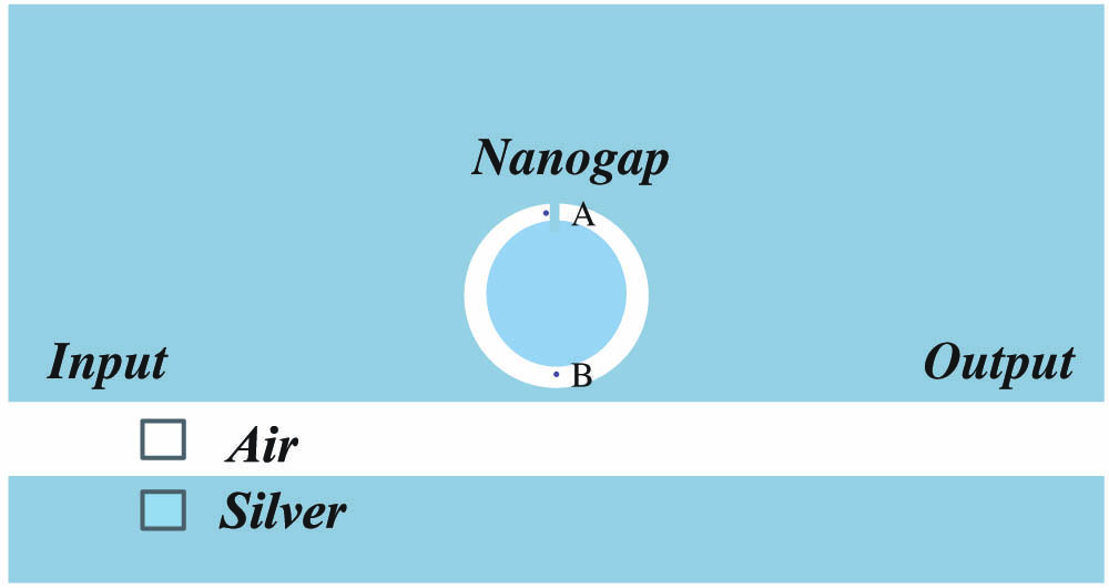
Figure 1.MIM structure studied in this paper. The waveguide and ring resonator have a width of 50 nm, the nearest distance between the two subjects is 10 nm, and the nanogap in the ring resonator is 2 nm. For convenience, here we give two points and to discuss later. The metal in this paper is . Its Drude parameter is high frequency relative permittivity , the plasma frequency is , and the plasma decay is .
The symmetric plasmonic nano-resonator supports two counterpropagating WGMs (CW and CCW). We use the annihilation (creation) operators () and () to symbolize these two counter-propagating WGMs. The Hamiltonian of the resonator system could be written as where denotes the eigenfrequency of the CW and CCW modes, and represents the coupling strength that is induced by the elastic Rayleigh scattering. Based on the Heisenberg equation, the equations for the motion of the system could be written as
Here and are the amplitude of the input CW and CCW fields, respectively. corresponds to the intrinsic damping in the mode, with being the intrinsic and external quality factors [9,10]. and are the fiber taper-resonator input and output coupling rate. Considering that the input and output coupling rate are different from each other for the existence of the standing wave, we give a numerical solution of the EM field in the following part. By applying the bosonic commutation relations, Eqs. (2) and (3) can be expressed as
Based on the dipole approximation of the scatterer in the subwavelength scattering (Rayleigh scattering) progress [31], the coupling coefficients could be written as
denotes the quantization volume of the WGM. is the mode function, and represents the polarizability of the scatterer with volume , and and represent electric permittivities of the particle and the surrounding medium, respectively. By replacing the modes of the resonator with and that of the input modes with [32–34], we find that in a steady-state regime the normal modes can be expressed as where denotes the laser-cavity detuning. Consider the system is single side pumped and denote the absence of the CCW input as . Based on the input–output relationship [35], we could solve the transmission coefficient of the coupled system as
As shown in the transmission coefficient, we assume the output coupling is related to both the position of the defect and the pumping frequency. For simplicity, if we take , then Eq. (9) can be expressed as
3. EFFECT OF FIELD DISTRIBUTION ON THE OUTPUT COUPLING RATE
When we consider both the existence of the CW and CCW modes, the standing wave condition could be satisfied. It is obvious that the standing wave field would be affected by both the position of the scatter and the pump frequency and the standard standing wave can be written as [36]
Here describes the relationship between the distribution of the field and the position of the detection point (theta). is the amplitude of the field, and the trigonometric function corresponds to the spatial dependence of the standing wave. represents the phase connected with the detection position. The terms and show that the phase of the system could be affected by the position of the scatter and the input field wavelength, respectively. Based on the numerical results of the field distribution, we give the phenomenological expression of these two parts ( and ).
In the following, we solve the electric field equations using the finite element method (FEM). The electric field in the two-dimensional MIM waveguide could be described as [31,36]
Here is the relative permeability, denotes the wave number, and stands for the wave number in the direction. Also represents the relative dielectric constant for the metal area, which is described by the Drude model as , with high frequency relative dielectric constant , plasma frequency , and decay . Here we choose Ag as the substrate material with the high frequency relative permittivity , the plasma frequency , and the plasma decay .

Figure 2.Electric field distribution of the input field with wavelength (a) 982 and (b) 1081 nm. Here we take the gap as the origin point and rotate around the ring resonator CCW with an angle of . The inset figure shows the field magnitude of the electric field.
In Fig. 2, we plot the distribution of the electric field in the ring cavity with a notch under the different position. The inset figure shows the field magnitude of the electric field. corresponds to the angle along the ring resonator in a CCW direction, and we take the gap as the starting point() in this figure. This distribution shows that the electric field distribution fits with the sinusoidal function. Considering the harmonic oscillatory and linear propagating feature of this structure and assuming that the high-order term of and are physically negligible, Eq. (11) can be written as where shows the maximal value of the electric field intensity in the ring cavity, and denotes that the standing wave is determined by the position of the scatter.
In Fig. 3, the electric field intensity at point is plotted under the condition that the scatter (gap) has different angles with point in the CCW direction. The EM field has twice the minimal and maximum values compared with Fig. 2 for both 982 and 1081 nm in the range of . The coupling rate between the cavity and waveguide is proportional to the electric field intensity in the near waveguide region. We notice that the output coupling strength starts to weaken when the wave loop is closed with the waveguide. A minimal point of the field intensity point also appears. The electric field at point also could be affected both by the cavity field strength and the detection position. The electric field at point is as shown in Fig. 2. The maximum electric field is connected to the mode amplitude . The coupling strength of the cavity and waveguide is decided by the scattering in the cavity. Compared with the electric field distribution shown in Eq. (13), we can write the as
Figure 3.Electric field distribution of the ring resonator in Fig. 1. The resonance wavelengths are (a) 982 and (b) 1081 nm. Here the gap is rotated CCW around the ring resonator from point .
4. GAP INDUCED MODE EVOLUTION ON THE TRANSMISSION SPECTRUM
To further explore the characteristics of this system, we study the transmission spectrum using the FEM. As shown in Fig. 4, we simulate both the perfect and the defect cavity condition with the defect at an angle of in the CW direction with point . We can conclude that in Fig. 4(a) there are several plasmonic modes in this structure. Meanwhile, the influence of mode coupling is shown in Fig. 4(b). Based on the distance of mode splitting, we can numerically find the coupling strength between CCW and CW modes. The transmission could also reveal the coupling strength between the cavity resonator and the waveguide. For the modes of 1081 nm, the coupling strength is 87.4 THz according to the numerical result in Fig. 4(b). The strong coupling comes from the strong mode energy change between the CW and CCW when the scatter is small. The FWHM in Fig. 4(a) shows that the intrinsic decay (the width of the Lorentz spectrum) of the WGMs is 8.9 THz. The input coupling strength between the waveguide and WGMs can be solved by fitting the minimum point of the coupling mode theory and input–the output relationship with the simulation value, and it is . We can write transmission equations [Eq. (9)] based on coupled mode theory as
Figure 4.Transmission spectrum of (a) a perfect ring resonator. (b) The nanogap has an angle of with point in the CCW direction.
As shown in Fig. 5, we plot the transmission spectrum based on both the coupled mode theory and FEM. It shows that the result of the coupled mode theory has high consistency with that of the FEM. The gap is placed at the angle in a CCW direction with point . The transmission is shown in Fig. 5(a), where the strength of mode is stronger than , which corresponds to the low transmission rate in mode(982 nm) but is high for mode(1081 nm). When the angle is , as shown in Fig. 5(b), the transmission rate will be approximately equal. When the angle is changed to , the situation is just the opposite and the transmission rate of the mode is quite weak compared to mode, as shown in Fig. 5(c). Both the transmission spectrum in Fig. 5 and the expression in Eq. (15) show that the transmission spectrum will change along with the position of the gap. It means the transmission spectrum can be modulated by the position of the gap (defect).
Figure 5.Simulation of spectrum using the coupled mode theory (solid lines) and the FEM (dashed lines) with a different angle between the gap and point . Here we take the CCW direction from to the gap as the positive direction. The angle is selected as (a) , (b) , and (c) .
Finally in Fig. 6, we plot the transmission spectrum with different defect positions as an inside walls defect in (a), an exinous defect in (b), and an in-cavity nano-tip (a defect not in touch with both the inner and outer walls of the cavity) in (c), which works as a scatter. We take the angle of the scatter to be the same as in Fig. 5(b). Under this condition, the strength of the and modes are comparable. In these figures, the difference in mode splitting can be attributed to the difference related to the strength of the Rayleigh scattering.
Figure 6.Transmission spectrum of the inside wall defect, in-ring defect, and exinous defect. Here we plot the transmission spectrum when the defects have an angle of with point in the CCW direction. The inset figure shows the distribution of the electric field in this structure with input wavelength 1081 nm. (a) The defect is in the inside wall. (b) The defect is exinous. (c) The defect is all in the ring cavity but does not touch the periphery of the cavity. The inset figure shows the field magnitude of the electric field.
5. CONCLUSION
In summary, we theoretically studied mode evolution in an asymmetric WGM plasmonic resonator system. We find the transmission spectrum of the plasmonic system can be tuned by the gap in the plasmonic resonator. We also give both the analytical and simulation calculation based on the coupled mode theory and the FEM. Both methods show that the transmission can be modulated by adjusting the gap position. On the other hand, the proposed method could further be applied for sensing and detecting the position of defects in WGM systems.
References
[1] H. Raether. Surface Plasmons on Smooth Surfaces(1988).
[2] M. Tame, K. McEnery, Ş. Özdemir, J. Lee, S. Maier, M. Kim. Quantum plasmonics. Nat. Phys., 9, 329-340(2013).
[3] M. Luchansky, R. Bailey. High-Q optical sensors for chemical and biological analysis. Anal. Chem., 84, 793-821(2012).
[4] A. Cetin, H. Altug. Fano resonant ring/disk plasmonic nanocavities on conducting substrates for advanced biosensing. ACS Nano, 6, 9989-9995(2012).
[5] . The Theory of Sound, 2(1896).
[6] G. Mie. Beiträge zur optik trüber medien, speziell kolloidaler metallösungen. Ann. Phys., 330, 377-445(1908).
[7] P. Debye. Der lichtdruck auf kugeln von beliebigem material. Ann. Phys., 335, 57-136(1909).
[8] I. Grudinin, V. Ilchenko, L. Maleki. Ultrahigh optical Q factors of crystalline resonators in the linear regime. Phys. Rev. A, 74, 063806(2006).
[9] M. Cai, O. Painter, K. Vahala. Observation of critical coupling in a fiber taper to a silica-microsphere whispering-gallery mode system. Phys. Rev. Lett., 85, 74-77(2000).
[10] S. Spillane, T. Kippenberg, O. Painter, K. Vahala. Ideality in a fiber-taper-coupled microresonator system for application to cavity quantum electrodynamics. Phys. Rev. Lett., 91, 043902(2003).
[11] S. Arnold, M. Khoshsima, I. Teraoka, S. Holler, F. Vollmer. Shift of whispering-gallery modes in microspheres by protein adsorption. Opt. Lett., 28, 272-274(2003).
[12] J. Zhu, S. Ozdemir, Y.-F. Xiao, L. Li, L. He, D.-R. Chen, L. Yang. On-chip single nanoparticle detection and sizing by mode splitting in an ultrahigh-Q microresonator. Nat. Photonics, 4, 46-49(2009).
[13] P. DelHaye, A. Schliesser, O. Arcizet, T. Wilken, R. Holzwarth, T. Kippenberg. Optical frequency comb generation from a monolithic microresonator. Nature, 450, 1214-1217(2007).
[14] T. Kippenberg, K. Vahala. Cavity optomechanics: back-action at the mesoscale. Science, 321, 1172-1176(2008).
[15] S. Weis, R. Rivière, S. Deléglise, E. Gavartin, O. Arcizet, A. Schliesser, T. J. Kippenberg. Optomechanically induced transparency. Science, 330, 1520-1523(2010).
[16] X. F. Liu, F. C. Lei, M. Gao, X. Yang, G. Q. Qin, G. L. Long. Fabrication of a microtoroidal resonator with picometer precise resonant wavelength. Opt. Lett., 41, 3603-3606(2016).
[17] B. Min, E. Ostby, V. Sorger, E. Ulin-Avila, L. Yang, X. Zhang, K. Vahala. High-Q surface-plasmon-polariton whispering-gallery microcavity. Nature, 457, 455-458(2009).
[18] A. Armani, R. Kulkarni, S. Fraser, R. Flagan, K. Vahala. Label-free, single-molecule detection with optical microcavities. Science, 317, 783-787(2007).
[19] F. Vollmer, S. Arnold. Whispering-gallery-mode biosensing: label-free detection down to single molecules. Nat. Methods, 5, 591-596(2008).
[20] F. Vollmer, S. Arnold, D. Keng. Single virus detection from the reactive shift of a whispering-gallery mode. Proc. Natl. Acad. Sci. USA, 105, 20701-20704(2008).
[21] X. C. Yu, B. B. Li, P. Wang, L. Tong, X. F. Jiang, Y. Li, Q. Gong, Y. F. Xiao. Single nanoparticle detection and sizing using a nanofiber pair in an aqueous environment. Adv. Mater., 26, 7462-7467(2014).
[22] Ş. Özdemir, J. Zhu, X. Yang, B. Peng, H. Yilmaz, L. He, F. Monifi, S. H. Huang, G. L. Long, L. Yang. Highly sensitive detection of nanoparticles with a self-referenced and self-heterodyned whispering-gallery Raman microlaser. Proc. Natl. Acad. Sci. USA, 111, E3836-E3844(2014).
[23] B. B. Li, W. Clements, X. C. Yu, K. Shi, Q. Gong, Y. F. Xiao. Single nanoparticle detection using split-mode microcavity Raman lasers. Proc. Natl. Acad. Sci. USA, 111, 14657-14662(2014).
[24] L. He, Ş. K. Özdemir, J. Zhu, W. Kim, L. Yang. Detecting single viruses and nanoparticles using whispering gallery microlasers. Nat. Nanotechnol., 6, 428-432(2011).
[25] J. Swaim, J. Knittel, W. Bowen. Detection limits in whispering gallery biosensors with plasmonic enhancement. Appl. Phys. Lett., 99, 243109(2011).
[26] E. Arbabi, S. Kamali, S. Arnold, L. Goddard. Hybrid whispering gallery mode/plasmonic chain ring resonators for biosensing. Appl. Phys. Lett., 105, 231107(2014).
[27] H. Hunt, A. Armani. Label-free biological and chemical sensors. Nanoscale, 2, 1544-1559(2010).
[28] J. Porto, F. Garcia-Vidal, J. Pendry. Transmission resonances on metallic gratings with very narrow slits. Phys. Rev. Lett., 83, 2845-2848(1999).
[29] H. Miyazaki, Y. Kurokawa. Squeezing visible light waves into a 3-nm-thick and 55-nm-long plasmon cavity. Phys. Rev. Lett., 96, 097401(2006).
[30] E. Verhagen, J. Dionne, L. Kuipers, H. Atwater, A. Polman. Near-field visualization of strongly confined surface plasmon polaritons in metal-insulator-metal waveguides. Nano Lett., 8, 2925-2929(2008).
[31] J. D. Jackson. Classical Electrodynamics, 3(1988).
[32] A. Yariv. Coupled-mode theory for guided-wave optics. IEEE J. Quantum Electron., 9, 919-933(1973).
[33] H. Haus, W. P. Huang. Coupled-mode theory. Proc. IEEE, 79, 1505-1518(1991).
[34] B. Peng, Ş. K. Özdemir, F. Lei, F. Monifi, M. Gianfreda, G. L. Long, S. Fan, F. Nori, C. M. Bender, L. Yang. Parity-time-symmetric whispering-gallery microcavities. Nat. Phys., 10, 394-398(2014).
[35] D. Walls, G. Milburn. Input–output formulation of optical cavities. Quantum Optics, 127-141(2008).
[36] D. Griffiths, R. College. Introduction to Electrodynamics, 3(1999).

