• Chinese Optics Letters
  • Vol. 20, Issue 1, 011602 (2022)
Huanhuan Su1, Huizhen Zhang1, Wenjing Wu2, Xiang Wang1, Guanghou Wang1, and Lin Zhou1、*
Author Affiliations
  • 1National Laboratory of Solid State Microstructures, School of Physics, College of Engineering and Applied Sciences, Nanjing University, Nanjing 210093, China
  • 2Department of Electrical Engineering, The Pennsylvania State University, University Park, Pennsylvania 16802, USA
  • show less
    DOI: 10.3788/COL202220.011602 Cite this Article Set citation alerts
    Huanhuan Su, Huizhen Zhang, Wenjing Wu, Xiang Wang, Guanghou Wang, Lin Zhou. Chemically engineered dendrite growth of uniform monolayers MoS2 for enhanced photoluminescence [Invited][J]. Chinese Optics Letters, 2022, 20(1): 011602 Copy Citation Text show less
    (a) Schematic diagram of the CVD setup for growth of MoS2. The locations of S, MoO3, and SiO2/Si substrate are exactly displayed. (b) Schematic of the growth of MoS2 with the extra H2O sources. (c) Schematic of the conventional triangular growth of MoS2 without H2O sources.
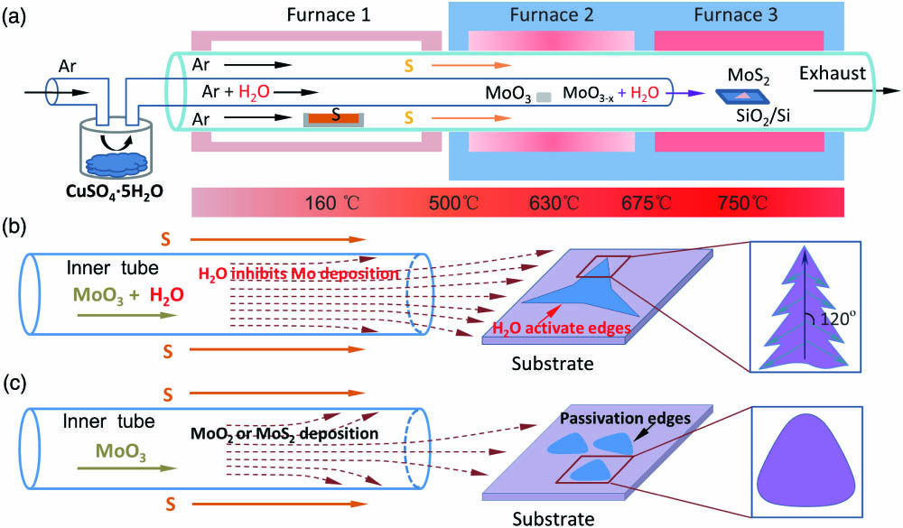
    Fig. 1. (a) Schematic diagram of the CVD setup for growth of MoS2. The locations of S, MoO3, and SiO2/Si substrate are exactly displayed. (b) Schematic of the growth of MoS2 with the extra H2O sources. (c) Schematic of the conventional triangular growth of MoS2 without H2O sources.
    (a), (e) Microscopic optical photographs, (b), (f) fluorescence spectra, (c), (g) phase diagrams of AFM images, and (d), (h) photoluminescence (PL) spectra for (a)–(c) dendrite and (e)–(g) conventional triangular monolayers MoS2, respectively. Scale bar: (a), (b) = 50 µm, (e), (f) = 10 µm, (c), (g) = 6 µm.
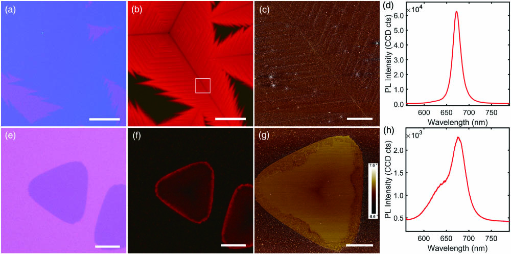
    Fig. 2. (a), (e) Microscopic optical photographs, (b), (f) fluorescence spectra, (c), (g) phase diagrams of AFM images, and (d), (h) photoluminescence (PL) spectra for (a)–(c) dendrite and (e)–(g) conventional triangular monolayers MoS2, respectively. Scale bar: (a), (b) = 50 µm, (e), (f) = 10 µm, (c), (g) = 6 µm.
    (a) Bright-field image of a uniform MoS2 dendrite with a large size. (b) Diffraction pattern of the area marked with black circle in (a) and the vector indicate the two families, KS and KMo. (c) Amplitude of the AFM image of the prepared monolayer MoS2 by water-assisted CVD procedure. (d) A line scan profile shows the diffraction intensity of framed spots in (b). (e) Representative Raman spectrum of the monolayer MoS2 dendrites grown on Si/SiO2 substrate. (f) shows the line profile along the white line in (c). The measured thickness of the monolayer is ∼1 nm.
    Fig. 3. (a) Bright-field image of a uniform MoS2 dendrite with a large size. (b) Diffraction pattern of the area marked with black circle in (a) and the vector indicate the two families, KS and KMo. (c) Amplitude of the AFM image of the prepared monolayer MoS2 by water-assisted CVD procedure. (d) A line scan profile shows the diffraction intensity of framed spots in (b). (e) Representative Raman spectrum of the monolayer MoS2 dendrites grown on Si/SiO2 substrate. (f) shows the line profile along the white line in (c). The measured thickness of the monolayer is ∼1 nm.
    (a) Schematic diagram of growth of MoS2 in the representative regions of I, II, III. (b)–(d) Optical microscopy (OM) images of the monolayer MoS2 in the regions of I, II, III, respectively. The domain evolves from the isolated monolayer in I to the continuous MoS2 flakes in III. (e)–(g) are the fluorescence spectroscopy (FM) images corresponding to (b)–(d), respectively. The intensity of fluorescence increases gradually from (e) to (g). (h) PL intensity in areas I, II, and III of the monolayer MoS2, respectively. Scale bars: 100 µm.
    Fig. 4. (a) Schematic diagram of growth of MoS2 in the representative regions of I, II, III. (b)–(d) Optical microscopy (OM) images of the monolayer MoS2 in the regions of I, II, III, respectively. The domain evolves from the isolated monolayer in I to the continuous MoS2 flakes in III. (e)–(g) are the fluorescence spectroscopy (FM) images corresponding to (b)–(d), respectively. The intensity of fluorescence increases gradually from (e) to (g). (h) PL intensity in areas I, II, and III of the monolayer MoS2, respectively. Scale bars: 100 µm.
    Analysis of the CVD-grown uniform dendritic monolayer MoS2 morphology. (a) Fluorescence microscope image for uniform dendritic monolayer MoS2. The hierarchical structures are marked by arrows, i.e., yellow for primary backbone, green and blue for the secondary and tertiary branches. The axial angles between different hierarchical branches (I and II, II, and III) have the same 120° angle. (b) The close-ups of areas marked by the solid rectangles in (a). (c) Atomic structure arrangement diagram of uniform dendritic MoS2. The region in the red circle has more defects, where fluorescence is stronger.
    Fig. 5. Analysis of the CVD-grown uniform dendritic monolayer MoS2 morphology. (a) Fluorescence microscope image for uniform dendritic monolayer MoS2. The hierarchical structures are marked by arrows, i.e., yellow for primary backbone, green and blue for the secondary and tertiary branches. The axial angles between different hierarchical branches (I and II, II, and III) have the same 120° angle. (b) The close-ups of areas marked by the solid rectangles in (a). (c) Atomic structure arrangement diagram of uniform dendritic MoS2. The region in the red circle has more defects, where fluorescence is stronger.
    Huanhuan Su, Huizhen Zhang, Wenjing Wu, Xiang Wang, Guanghou Wang, Lin Zhou. Chemically engineered dendrite growth of uniform monolayers MoS2 for enhanced photoluminescence [Invited][J]. Chinese Optics Letters, 2022, 20(1): 011602
    Download Citation