
Huanhuan Su, Huizhen Zhang, Wenjing Wu, Xiang Wang, Guanghou Wang, Lin Zhou, "Chemically engineered dendrite growth of uniform monolayers MoS2 for enhanced photoluminescence [Invited]," Chin. Opt. Lett. 20, 011602 (2022)
- Chinese Optics Letters
- Vol. 20, Issue 1, 011602 (2022)
Abstract
1. Introduction
Atomically thin two-dimensional (2D) transition metal dichalcogenides (TMDs)-like monolayer
2. Fabrication Process and Design
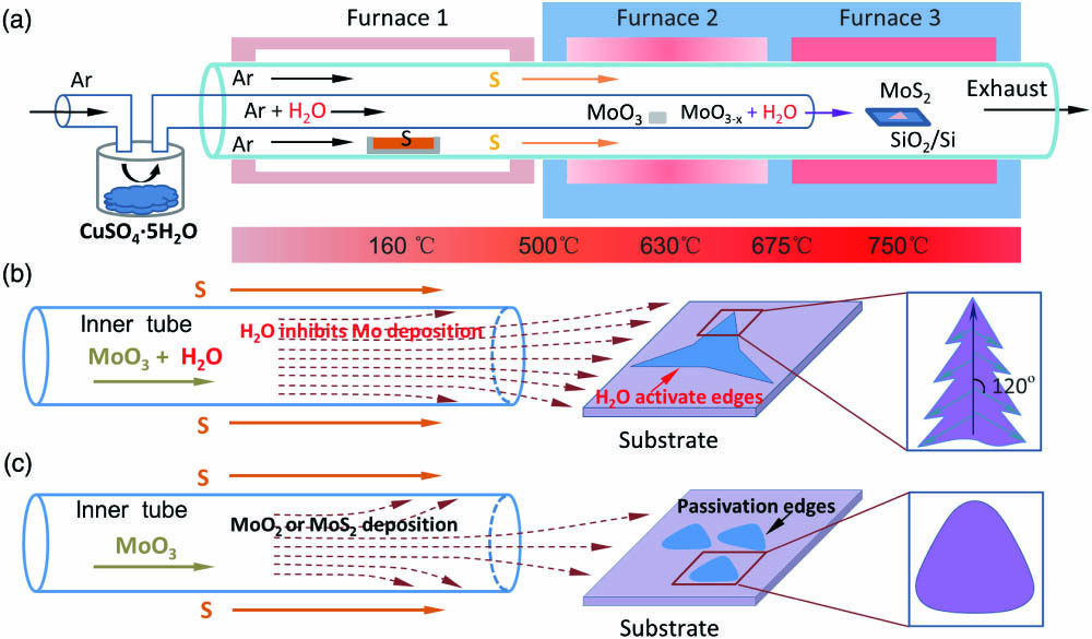
Figure 1(a) schematically illustrates the rationally-designed three-zone CVD setup for the large area dendrite-type growth of monolayer
![]()
Figure 1.(a) Schematic diagram of the CVD setup for growth of MoS2. The locations of S, MoO3, and SiO2/Si substrate are exactly displayed. (b) Schematic of the growth of MoS2 with the extra H2O sources. (c) Schematic of the conventional triangular growth of MoS2 without H2O sources.
3. Chemically Engineered Photoluminescence
The representative optical images of as-grown dendrite-type monolayer
Sign up for Chinese Optics Letters TOC. Get the latest issue of Chinese Optics Letters delivered right to you!Sign up now
![]()
Figure 2.(a), (e) Microscopic optical photographs, (b), (f) fluorescence spectra, (c), (g) phase diagrams of AFM images, and (d), (h) photoluminescence (PL) spectra for (a)–(c) dendrite and (e)–(g) conventional triangular monolayers MoS2, respectively. Scale bar: (a), (b) = 50 µm, (e), (f) = 10 µm, (c), (g) = 6 µm.
![]()
Figure 3.(a) Bright-field image of a uniform MoS2 dendrite with a large size. (b) Diffraction pattern of the area marked with black circle in (a) and the vector indicate the two families, KS and KMo. (c) Amplitude of the AFM image of the prepared monolayer MoS2 by water-assisted CVD procedure. (d) A line scan profile shows the diffraction intensity of framed spots in (b). (e) Representative Raman spectrum of the monolayer MoS2 dendrites grown on Si/SiO2 substrate. (f) shows the line profile along the white line in (c). The measured thickness of the monolayer is ∼1 nm.
In order to identify the crystalline structure of dendrite
The role of trace water induced chemical corrosion, as well as the off-stoichiometric-ratio dendrite growth, can further be inferred from the position-dependent fluorescence images of monolayer
![]()
Figure 4.(a) Schematic diagram of growth of MoS2 in the representative regions of I, II, III. (b)–(d) Optical microscopy (OM) images of the monolayer MoS2 in the regions of I, II, III, respectively. The domain evolves from the isolated monolayer in I to the continuous MoS2 flakes in III. (e)–(g) are the fluorescence spectroscopy (FM) images corresponding to (b)–(d), respectively. The intensity of fluorescence increases gradually from (e) to (g). (h) PL intensity in areas I, II, and III of the monolayer MoS2, respectively. Scale bars: 100 µm.
Finally, to unravel the physical mechanism of the dendrite-type growth of monolayer
![]()
Figure 5.Analysis of the CVD-grown uniform dendritic monolayer MoS2 morphology. (a) Fluorescence microscope image for uniform dendritic monolayer MoS2. The hierarchical structures are marked by arrows, i.e., yellow for primary backbone, green and blue for the secondary and tertiary branches. The axial angles between different hierarchical branches (I and II, II, and III) have the same 120° angle. (b) The close-ups of areas marked by the solid rectangles in (a). (c) Atomic structure arrangement diagram of uniform dendritic MoS2. The region in the red circle has more defects, where fluorescence is stronger.
4. Conclusion
In conclusion, we experimentally evidenced the large area dendrite-type monolayer
5. Methods
5.1. Preparation and transfer of monolayer
5.2. Sample characterization
TEM characterizations were carried out on TECNAI F20. Raman and PL spectroscopies and mapping were carried out using a WITEC Alpha 300 micro-Raman confocal microscope, with the diode laser operating at a wavelength of 532 nm. A
References
[1] M. A. R. Anjum, H. Y. Jeong, M. H. Lee, H. S. Shin, J. S. Lee. Efficient hydrogen evolution reaction catalysis in alkaline media by all-in-one MoS2 with multifunctional active sites. Adv. Mater., 30, 1707105(2018).
[2] X. Wang, Y. Zhang, H. Si, Q. Zhang, J. Wu, L. Gao, X. Wei, Y. Sun, Q. Liao, Z. Zhang, K. Ammarah, L. Gu, Z. Kang, Y. Zhang. Single-atom vacancy defect to trigger high-efficiency hydrogen evolution of MoS2. J. Am. Chem. Soc., 142, 4298(2020).
[3] Q. C. Wang, Y. P. Lei, Y. C. Wang, Y. Liu, C. Y. Song, J. Zeng, Y. H. Song, X. D. Duan, D. S. Wang, Y. D. Li. Atomic-scale engineering of chemical-vapor-deposition-grown 2D transition metal dichalcogenides for electrocatalysis. Energy Environ. Sci., 13, 1593(2020).
[4] F. Bonaccorso, A. Lombardo, T. Hasan, Z. Sun, L. Colombo, A. C. Ferrari. Production and processing of graphene and 2D crystals. Mater. Today, 15, 564(2012).
[5] S. B. Desai, S. R. Madhvapathy, M. Amani, D. Kiriya, M. Hettick, M. Tosun, Y. Zhou, M. Dubey, J. W. Ager, D. Chrzan, A. Javey. Gold-mediated exfoliation of ultralarge optoelectronically-perfect monolayers. Adv. Mater., 28, 4053(2016).
[6] B. Radisavljevic, A. Radenovic, J. Brivio, V. Giacometti, A. Kis. Single-layer MoS2 transistors. Nat. Nanotechnol., 6, 147(2011).
[7] Q. A. Vu, W. J. Yu. Electronics and optoelectronics based on two-dimensional materials. J. Korean Phys. Soc., 73, 1(2018).
[8] R. Maiti, C. Patil, M. A. S. R. Saadi, T. Xie, J. G. Azadani, B. Uluutku, R. Amin, A. F. Briggs, M. Miscuglio, D. Van Thourhout, S. D. Solares, T. Low, R. Agarwal, S. R. Bank, V. J. Sorger. Strain-engineered high-responsivity MoTe2 photodetector for silicon photonic integrated circuits. Nat. Photonics, 14, 578(2020).
[9] K. F. Mak, C. Lee, J. Hone, J. Shan, T. F. Heinz. Atomically thin MoS2: a new direct-gap semiconductor. Phys. Rev. Lett., 105, 136805(2010).
[10] K. S. Novoselov, D. Jiang, F. Schedin, T. J. Booth, V. V. Khotkevich, S. V. Morozov, A. K. Geim. Two-dimensional atomic crystals. Proc. Natl Acad. Sci. USA, 102, 10451(2005).
[11] A. Splendiani, L. Sun, Y. Zhang, T. Li, J. Kim, C. Y. Chim, G. Galli, F. Wang. Emerging photoluminescence in monolayer MoS2. Nano Lett., 10, 1271(2010).
[12] F. Withers, O. Del Pozo-Zamudio, A. Mishchenko, A. P. Rooney, A. Gholinia, K. Watanabe, T. Taniguchi, S. J. Haigh, A. K. Geim, A. Tartakovskii, K. S. Novoselov. Light-emitting diodes by band-structure engineering in van der Waals heterostructures. Nat. Mater., 14, 301(2015).
[13] E. M. Alexeev, D. A. Ruiz-Tijerina, M. Danovich, M. J. Hamer, D. J. Terry, P. K. Nayak, S. Ahn, S. Pak, J. Lee, J. I. Sohn, M. R. Molas, M. Koperski, K. Watanabe, T. Taniguchi, K. S. Novoselov, R. V. Gorbachev, H. S. Shin, V. I. Fal’ko, A. I. Tartakovskii. Resonantly hybridized excitons in Moire superlattices in van der Waals heterostructures. Nature, 567, 81(2019).
[14] M. Onodera, S. Masubuchi, R. Moriya, T. Machida. Assembly of van der Waals heterostructures: exfoliation, searching, and stacking of 2D materials. Jpn. J. Appl. Phys., 59, 1(2020).
[15] Y. Wakafuji, R. Moriya, S. Masubuchi, K. Watanabe, T. Taniguchi, T. Machida. 3D manipulation of 2D materials using microdome polymer. Nano Lett., 20, 2486(2020).
[16] S. Masubuchi, M. Morimoto, S. Morikawa, M. Onodera, Y. Asakawa, K. Watanabe, T. Taniguchi, T. Machida. Autonomous robotic searching and assembly of two-dimensional crystals to build van der Waals superlattices. Nat. Commun., 9, 1413(2018).
[17] Y. Jung, E. Ji, A. Capasso, G. H. Lee. Recent progresses in the growth of two-dimensional transition metal dichalcogenides. J. Korean Ceram. Soc., 56, 24(2019).
[18] Y. Zhang, Y. Yao, M. G. Sendeku, L. Yin, X. Zhan, F. Wang, Z. Wang, J. He. Recent progress in CVD growth of 2D transition metal dichalcogenides and related heterostructures. Adv. Mater., 31, 1901694(2019).
[19] X. Zhang, H. Nan, S. Xiao, X. Wan, Z. Ni, X. Gu, K. Ostrikov. Shape-uniform, high-quality monolayered MoS2 crystals for gate-tunable photoluminescence. ACS Appl. Mater. Interfaces, 9, 42121(2017).
[20] T. Li, W. Guo, L. Ma, W. Li, Z. Yu, Z. Han, S. Gao, L. Liu, D. Fan, Z. Wang, Y. Yang, W. Lin, Z. Luo, X. Chen, N. Dai, X. Tu, D. Pan, Y. Yao, P. Wang, Y. Nie, J. Wang, Y. Shi, X. Wang. Epitaxial growth of wafer-scale molybdenum disulfide semiconductor single crystals on sapphire. Nat. Nanotechnol.(2021).
[21] D. H. Lien, S. Z. Uddin, M. Yeh, M. Amani, H. Kim, J. W. Ager, E. Yablonovitch, A. Javey. Electrical suppression of all nonradiative recombination pathways in monolayer semiconductors. Science, 364, 468(2019).
[22] W. Su, L. Jin, X. Qu, D. Huo, L. Yang. Defect passivation induced strong photoluminescence enhancement of rhombic monolayer MoS2. Phys. Chem. Chem. Phys., 18, 14001(2016).
[23] W. Xu, S. Li, S. Zhou, J. K. Lee, S. Wang, S. G. Sarwat, X. Wang, H. Bhaskaran, M. Pasta, J. H. Warner. Large dendritic monolayer MoS2 grown by atmospheric pressure chemical vapor deposition for electrocatalysis. ACS Appl. Mater. Interfaces, 10, 4630(2018).
[24] J. Ma, X. Li, L. Gan, S. Zhang, Y. Cao, Z. Nie, X. Wang, D. Ma, L. He, J. Nie, C. Xiong, R. Dou. Controlling the dendritic structure and the photo-electrocatalytic properties of highly crystalline MoS2 on sapphire substrate. 2D Materials, 5, 3(2018).
[25] C. R. Dean, A. F. Young, I. Meric, C. Lee, L. Wang, S. Sorgenfrei, K. Watanabe, T. Taniguchi, P. Kim, K. L. Shepard, J. Hone. Boron nitride substrates for high-quality graphene electronics. Nat. Nanotechnol., 5, 722(2010).
[26] I. S. Kim, V. K. Sangwan, D. Jariwala, J. D. Wood, S. Park, K. S. Chen, F. Shi, F. Ruiz-Zepeda, A. Ponce, M. Jose-Yacaman, V. P. Dravid, T. J. Marks, M. C. Hersam, L. J. Lauhon. Influence of stoichiometry on the optical and electrical properties of chemical vapor deposition derived MoS2. ACS Nano, 8, 10551(2014).
[27] H. Liu, J. Lu, K. Ho, Z. Hu, Z. Dang, A. Carvalho, H. R. Tan, E. S. Tok, C. H. Sow. Fluorescence concentric triangles: a case of chemical heterogeneity in WS2 atomic monolayer. Nano Lett., 16, 5559(2016).
[28] K. Wu, Z. Li, J. B. Tang, X. L. Lv, H. L. Wang, R. C. Luo, P. Liu, L. H. Qian, S. P. Zhang, S. L. Yuan. Controllable defects implantation in MoS2 grown by chemical vapor deposition for photoluminescence enhancement. Nano Res., 11, 4123(2018).
[29] P. K. Sahoo, S. Memaran, Y. Xin, L. Balicas, H. R. Gutierrez. One-pot growth of two-dimensional lateral heterostructures via sequential edge-epitaxy. Nature, 553, 63(2018).
[30] X. Cui, L. Sun, Y. Zeng, Y. Hao, Y. Liu, D. Wang, Y. Yi, K. P. Loh, J. Zheng, Y. Liu. Visualization of crystallographic orientation and twist angles in two-dimensional crystals with an optical microscope. Nano Lett., 20, 6059(2020).
[31] M. Li, J. Shi, L. Liu, P. Yu, N. Xi, Y. Wang. Experimental study and modeling of atomic-scale friction in zigzag and armchair lattice orientations of MoS2. Sci. Technol. Adv. Mater., 17, 189(2016).
[32] R. Garcia, R. Magerle, R. Perez. Nanoscale compositional mapping with gentle forces. Nat. Mater., 6, 405(2007).
[33] H. Liu, J. Lu, K. Ho, Z. Hu, Z. Dang, A. Carvalho, H. R. Tan, E. S. Tok, C. H. Sow. Fluorescence concentric triangles: a case of chemical heterogeneity in WS2 atomic monolayer. Nano Lett., 16, 5559(2016).


Set citation alerts for the article
Please enter your email address

© Copyright 2018-2021 | Chinese Laser Press. All Rights Reserved 沪ICP备15018463号-20