Xuanhu Chen, Fangfang Ren, Shulin Gu, Jiandong Ye, "Review of gallium-oxide-based solar-blind ultraviolet photodetectors," Photonics Res. 7, 381 (2019)

Search by keywords or author
- Photonics Research
- Vol. 7, Issue 4, 381 (2019)

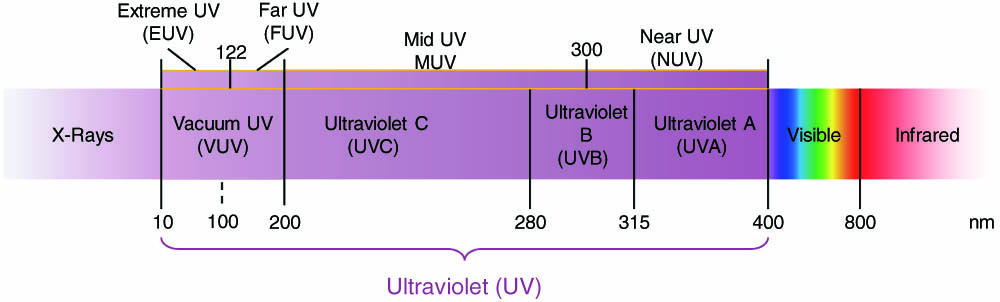
Fig. 1. UV spectral region and its subdivisions.

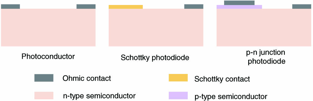
Fig. 2. Schematic structures of different semiconductor photodetectors.

Fig. 3. (a) Energy band diagram of a metal and a semiconductor before contact; (b) ideal energy band diagram of a metal/n–semiconductor junction for ϕ m > ϕ s .

Fig. 4. Dependence of the Schottky barrier height on the metal work function of different metals, and the ideal Schottky barrier height based on the Schottky–Mott model (short dashed curve).
![Chart illustrating transformation relationships among the forms of Ga2O3 and its hydrates. Redraw with permission from Roy et al. [93]. Copyright 1952 American Chemical Society.](/Images/icon/loading.gif)
Fig. 5. Chart illustrating transformation relationships among the forms of Ga 2 O 3 and its hydrates. Redraw with permission from Roy et al. [93]. Copyright 1952 American Chemical Society.
![Various Ga2O3 nanostructures. (a) γ-Ga2O3 nanocrystals. Reprinted with permission from Wang et al. [196]. Copyright 2010 American Chemical Society. (b) β-Ga2O3 nanowires. Reprinted with permission from Nogales et al. [229]. Copyright 2007 American Institute of Physics. (c) Ga2O3/GaN:Ox@SnO2 shell@core NWs. Reprinted with permission from Lupan et al. [234]. Copyright 2015 Elsevier B.V. (d) β-Ga2O3 nanorods. Reprinted with permission from Vanithakumari et al. [244]. Copyright 2009 Wiley-VCH Verlag GmbH & Co. KGaA, Weinheim. (e) As-synthesized β-Ga2O3 nanobelt. Reprinted with permission from Zou et al. [256]. Copyright 2014 Wiley-VCH Verlag GmbH & Co. KGaA, Weinheim. (f) Branched multiwire nanostructures (left) and its X-ray fluorescence (XRF) map (right). Reprinted with permission from Martinez-Criado et al. [224]. Copyright 2014 American Chemical Society.](/Images/icon/loading.gif)
Fig. 6. Various Ga 2 O 3 nanostructures. (a) γ - Ga 2 O 3 nanocrystals. Reprinted with permission from Wang et al. [196]. Copyright 2010 American Chemical Society. (b) β - Ga 2 O 3 nanowires. Reprinted with permission from Nogales et al. [229]. Copyright 2007 American Institute of Physics. (c) Ga 2 O 3 / GaN : O x @ SnO 2 shell@core NWs. Reprinted with permission from Lupan et al. [234]. Copyright 2015 Elsevier B.V. (d) β - Ga 2 O 3 nanorods. Reprinted with permission from Vanithakumari et al. [244]. Copyright 2009 Wiley-VCH Verlag GmbH & Co. KGaA, Weinheim. (e) As-synthesized β - Ga 2 O 3 nanobelt. Reprinted with permission from Zou et al. [256]. Copyright 2014 Wiley-VCH Verlag GmbH & Co. KGaA, Weinheim. (f) Branched multiwire nanostructures (left) and its X-ray fluorescence (XRF) map (right). Reprinted with permission from Martinez-Criado et al. [224]. Copyright 2014 American Chemical Society.

Fig. 7. The crystal structure of β - Ga 2 O 3 and its ( 2 ¯ 01 ) surfaces.
![Band structure of β-Ga2O3. (a) At the GGA–DFT (PBE) level and (b) at the hybrid HF–DFT (Gau–PBE) level. Reprinted with permission from Mock et al. [275]. Copyright 2017 American Physical Society.](/Images/icon/loading.gif)
Fig. 8. Band structure of β - Ga 2 O 3 . (a) At the GGA–DFT (PBE) level and (b) at the hybrid HF–DFT (Gau–PBE) level. Reprinted with permission from Mock et al. [275]. Copyright 2017 American Physical Society.
![(αhν)2 versus hν plots for (a) (010) Mg-doped substrate for E||c (closed circles) and E||a* (open circles) at RT. (b) Data set of (001) undoped substrate for E||a (closed squares) and E||b (open squares). Dotted lines represent the energies of the direct absorption edge. Partially polarized reflectance spectra at RT are shown in the upper part of the figures. Energies of the dips and the shoulder are indicated by the vertical arrows. Reprinted with permission from Onuma et al. [12]. Copyright 2015 The Japan Society of Applied Physics.](/Images/icon/loading.gif)
Fig. 9. ( α h ν ) 2 versus h ν plots for (a) (010) Mg-doped substrate for E | | c (closed circles) and E | | a * (open circles) at RT. (b) Data set of (001) undoped substrate for E | | a (closed squares) and E | | b (open squares). Dotted lines represent the energies of the direct absorption edge. Partially polarized reflectance spectra at RT are shown in the upper part of the figures. Energies of the dips and the shoulder are indicated by the vertical arrows. Reprinted with permission from Onuma et al. [12]. Copyright 2015 The Japan Society of Applied Physics.
![(a) 1 μm×1 μm scan image of an annealed surface observed by tapping mode atomic force microscopy. (b) I–V characteristics of a photodetector. Closed (black) and open (red) symbols represent current in the dark condition and current in the presence of 250 nm light irradiation, respectively. (c) Photocurrent spectral response (blue) and photoresponsivity of the photodetector (black) at a reverse bias of 10 V. The dashed line indicates the photoresponsivities expected in the case without carrier multiplication. Reprinted with permission from Oshima et al. [304]. Copyright 2008 The Japan Society of Applied Physics. (d) Transient response of the detector. (e) Signal from the flame detection system during the demonstration. Reprinted with permission from Oshima et al. [305]. Copyright 2009 The Japan Society of Applied Physics.](/Images/icon/loading.gif)
Fig. 10. (a) 1 μm × 1 μm scan image of an annealed surface observed by tapping mode atomic force microscopy. (b) I –V characteristics of a photodetector. Closed (black) and open (red) symbols represent current in the dark condition and current in the presence of 250 nm light irradiation, respectively. (c) Photocurrent spectral response (blue) and photoresponsivity of the photodetector (black) at a reverse bias of 10 V. The dashed line indicates the photoresponsivities expected in the case without carrier multiplication. Reprinted with permission from Oshima et al. [304]. Copyright 2008 The Japan Society of Applied Physics. (d) Transient response of the detector. (e) Signal from the flame detection system during the demonstration. Reprinted with permission from Oshima et al. [305]. Copyright 2009 The Japan Society of Applied Physics.
![(a) Dark I–V characteristics of the Au-Ga2O3 Schottky photodiode annealed at various temperatures. The inset shows the device configuration. (b) Spectral responsivities of the photodiode annealed at 400°C and the as-fabricated photodiode at a reverse bias of 3 V. The inset shows the photocurrent of the devices under reverse bias voltage to 5 V. Reprinted with permission from Suzuki et al. [87]. Copyright 2009 American Institute of Physics. (c) Time-dependent photoresponse of the β-Ga2O3 thin films prototype photodetector to 254 nm illumination: (top) the Ohmic-type device; (bottom) the Schottky-type device. Reprinted with permission from Guo et al. [310]. Copyright 2014 American Institute of Physics. (d) Temporal response tests of the PDs with KrF pulse laser illumination at 10 V bias. Reprinted with permission from Cui et al. [315]. Copyright 2017 Wiley-VCH Verlag GmbH & Co. KGaA, Weinheim.](/Images/icon/loading.gif)
Fig. 11. (a) Dark I –V characteristics of the Au - Ga 2 O 3 Schottky photodiode annealed at various temperatures. The inset shows the device configuration. (b) Spectral responsivities of the photodiode annealed at 400°C and the as-fabricated photodiode at a reverse bias of 3 V. The inset shows the photocurrent of the devices under reverse bias voltage to 5 V. Reprinted with permission from Suzuki et al. [87]. Copyright 2009 American Institute of Physics. (c) Time-dependent photoresponse of the β - Ga 2 O 3 thin films prototype photodetector to 254 nm illumination: (top) the Ohmic-type device; (bottom) the Schottky-type device. Reprinted with permission from Guo et al. [310]. Copyright 2014 American Institute of Physics. (d) Temporal response tests of the PDs with KrF pulse laser illumination at 10 V bias. Reprinted with permission from Cui et al. [315]. Copyright 2017 Wiley-VCH Verlag GmbH & Co. KGaA, Weinheim.
![(a) Photoresponsivity of metal–semiconductor–metal deep ultraviolet photodetectors. (b) Low-frequency noise power density as a function of frequency of metal–semiconductor–metal deep-ultraviolet photodetectors. Reprinted with permission from Lee et al. [320]. Copyright 2018 IEEE. (c) EDX line scan along the In gradient (the black dashed lines separate different crystallographic phases); (d) single XRD patterns selected from each phase. (e) Responsivity versus photon energy of 10 MSM-PDs along the In gradient. (f) Spectrally resolved J–V measurements of an SC [the analyzed ϕBn,eff are shown as squares in (e)]. Reprinted with permission from Zhang et al. [326]. Copyright 2016 American Institute of Physics.](/Images/icon/loading.gif)
Fig. 12. (a) Photoresponsivity of metal–semiconductor–metal deep ultraviolet photodetectors. (b) Low-frequency noise power density as a function of frequency of metal–semiconductor–metal deep-ultraviolet photodetectors. Reprinted with permission from Lee et al. [320]. Copyright 2018 IEEE. (c) EDX line scan along the In gradient (the black dashed lines separate different crystallographic phases); (d) single XRD patterns selected from each phase. (e) Responsivity versus photon energy of 10 MSM-PDs along the In gradient. (f) Spectrally resolved J –V measurements of an SC [the analyzed ϕ Bn , eff are shown as squares in (e)]. Reprinted with permission from Zhang et al. [326]. Copyright 2016 American Institute of Physics.
![(a) Real-time photoresponse of the detector to 254 nm light. (b) Enlarged rise and decay edges for the first “ON” and “OFF”, respectively. Reprinted with permission from Feng et al. [266]. Copyright 2006 American Institute of Physics. (c) Enlarged SEM images of the photo switch made of an individual Au-in-Ga2O3 peapod nanowire. (d) Photoresponse behaviors during illumination ON and OFF cycles between electrodes 11–13. Reprinted with permission from Hsieh et al. [207]. Copyright 2008 American Chemical Society.](/Images/icon/loading.gif)
Fig. 13. (a) Real-time photoresponse of the detector to 254 nm light. (b) Enlarged rise and decay edges for the first “ON” and “OFF”, respectively. Reprinted with permission from Feng et al. [266]. Copyright 2006 American Institute of Physics. (c) Enlarged SEM images of the photo switch made of an individual Au - in - Ga 2 O 3 peapod nanowire. (d) Photoresponse behaviors during illumination ON and OFF cycles between electrodes 11–13. Reprinted with permission from Hsieh et al. [207]. Copyright 2008 American Chemical Society.
![(a) Time-dependent photoresponse of the bridged β-Ga2O3 NWs grown at 925°C (sample 2, solid line) and at 800°C (sample 3, dotted line) measured in dry air under a bias voltage of 5 V and a UVC (254 nm) irradiance of ∼2 mW· cm−2. The photocurrent to dark current ratios for sample 2 and sample 3 were ∼5×10⁴ and ∼5×10⁶, respectively. (b) Spectral responses of sample 1 (squares), sample 2 (circles), and sample 3 (triangles). (c) Room-temperature PL spectra of sample 1 (solid line), sample 2 (dashed line), and sample 3 (dotted line), revealing an increase in defect emissions with decreasing growth temperature. (d) Time-dependent photoresponse of the bridged β-Ga2O3 NWs (sample 1). Reprinted with permission from Li et al. [331]. Copyright 2010 Wiley-VCH Verlag GmbH & Co. KGaA, Weinheim. (e) Schematic illustration of the fabrication of the β-Ga2O3 nanowire array film and its vertical Schottky photodiode. (f) I−V characteristics of the device in the dark and under the illumination of 254 nm light in the logarithmic scale. Inset shows the photovoltaic characteristic of the device near zero bias. (g) Time-dependent photocurrent response of an Au/β-Ga2O3 nanowire array film Schottky photodiode measured under 254 nm light illumination with the intensity of 2 mW·cm−2 at 0 V. (h) Decay edge of the current response at a reverse bias of 10 V. Reprinted with permission from Chen et al. [203]. Copyright 2016 American Chemical Society.](/Images/icon/loading.gif)
Fig. 14. (a) Time-dependent photoresponse of the bridged β - Ga 2 O 3 NWs grown at 925°C (sample 2, solid line) and at 800°C (sample 3, dotted line) measured in dry air under a bias voltage of 5 V and a UVC (254 nm) irradiance of ∼ 2 mW · cm − 2 . The photocurrent to dark current ratios for sample 2 and sample 3 were ∼ 5 × 10 4 and ∼ 5 × 10 6 , respectively. (b) Spectral responses of sample 1 (squares), sample 2 (circles), and sample 3 (triangles). (c) Room-temperature PL spectra of sample 1 (solid line), sample 2 (dashed line), and sample 3 (dotted line), revealing an increase in defect emissions with decreasing growth temperature. (d) Time-dependent photoresponse of the bridged β - Ga 2 O 3 NWs (sample 1). Reprinted with permission from Li et al. [331]. Copyright 2010 Wiley-VCH Verlag GmbH & Co. KGaA, Weinheim. (e) Schematic illustration of the fabrication of the β - Ga 2 O 3 nanowire array film and its vertical Schottky photodiode. (f) I −V characteristics of the device in the dark and under the illumination of 254 nm light in the logarithmic scale. Inset shows the photovoltaic characteristic of the device near zero bias. (g) Time-dependent photocurrent response of an Au / β - Ga 2 O 3 nanowire array film Schottky photodiode measured under 254 nm light illumination with the intensity of 2 mW · cm − 2 at 0 V. (h) Decay edge of the current response at a reverse bias of 10 V. Reprinted with permission from Chen et al. [203]. Copyright 2016 American Chemical Society.
![(a) Atomic force microscopy image of a 2D β-Ga2O3 photodetector; inset, the corresponding height profile of the photodetector. Reprinted with permission from Feng et al. [258]. Copyright 2014 Royal Society of Chemistry. (b) I–V characteristics of the device in the dark. (c) I–V characteristics of the device under irradiation with 254 nm light at different light intensities. Reprinted with permission from Zhong et al. [259]. Copyright 2015 Elsevier B.V. All rights reserved. (d) The ON/OFF cycle of the β-Ga2O3 nanobelt device upon 250 nm light illumination from the RT to 433 K under the intensity of 9.835×10⁻⁵ W/cm2 at a bias of 6.0 V. Reprinted with permission from Zou et al. [256]. Copyright 2014 Wiley-VCH Verlag GmbH & Co. KGaA, Weinheim. (e) Time-dependent photoresponse of the fabricated photodetector under various illumination conditions (254, 365, 532, and 650 nm light exposure). (f) Experimental and fitted curves of the current rise and decay process at 254 nm illumination under a gate bias of 0 V. Reprinted with permission from Oh et al. [169]. Copyright 2016 Royal Society of Chemistry.](/Images/icon/loading.gif)
Fig. 15. (a) Atomic force microscopy image of a 2D β - Ga 2 O 3 photodetector; inset, the corresponding height profile of the photodetector. Reprinted with permission from Feng et al. [258]. Copyright 2014 Royal Society of Chemistry. (b) I –V characteristics of the device in the dark. (c) I –V characteristics of the device under irradiation with 254 nm light at different light intensities. Reprinted with permission from Zhong et al. [259]. Copyright 2015 Elsevier B.V. All rights reserved. (d) The ON/OFF cycle of the β - Ga 2 O 3 nanobelt device upon 250 nm light illumination from the RT to 433 K under the intensity of 9.835 × 10 − 5 W / cm 2 at a bias of 6.0 V. Reprinted with permission from Zou et al. [256]. Copyright 2014 Wiley-VCH Verlag GmbH & Co. KGaA, Weinheim. (e) Time-dependent photoresponse of the fabricated photodetector under various illumination conditions (254, 365, 532, and 650 nm light exposure). (f) Experimental and fitted curves of the current rise and decay process at 254 nm illumination under a gate bias of 0 V. Reprinted with permission from Oh et al. [169]. Copyright 2016 Royal Society of Chemistry.
![(a) Schematic diagram of the APD device. (b) I–V characteristics of the photodetector under dark and illumination conditions with 254 nm light of 1.67 mW/cm2. (c) I–V characteristics at 300, 330, and 370 K in the reverse voltage under the dark condition; the inset shows the dependence of the avalanche breakdown voltage on the recording temperature. (d) Spectral response of the device at −6 V bias. (e) Transient response of the device at −6 V bias and a second-order exponential fit of the data. (f) Energy band diagram of the APD device in reverse bias. Reprinted with permission from Zhao et al. [240]. Copyright 2015 American Chemical Society.](/Images/icon/loading.gif)
Fig. 16. (a) Schematic diagram of the APD device. (b) I –V characteristics of the photodetector under dark and illumination conditions with 254 nm light of 1.67 mW / cm 2 . (c) I –V characteristics at 300, 330, and 370 K in the reverse voltage under the dark condition; the inset shows the dependence of the avalanche breakdown voltage on the recording temperature. (d) Spectral response of the device at − 6 V bias. (e) Transient response of the device at − 6 V bias and a second-order exponential fit of the data. (f) Energy band diagram of the APD device in reverse bias. Reprinted with permission from Zhao et al. [240]. Copyright 2015 American Chemical Society.
![(a) Dependence of current–voltage characteristics on intensity of UV light illumination of a deuterium lamp. (b) Top, reverse-current response of a photodiode to deep-UV light pulses (reverse-bias voltage is 2 V); bottom, light waveform measured by a silicon pin photodiode for the same light pulses. Reprinted with permission from Nakagomi et al. [342]. Copyright 2013 American Institute of Physics. (c) Spectral response of photodiodes based on a β-Ga2O3/GaN heterojunction with 116 nm and 175 nm thick β-Ga2O3 layers and based on a β-Ga2O3/SiC heterojunction with a 116 nm β-Ga2O3 layer. (d) Top, response of a photodiode to deep-UV light pulses with a reverse-bias voltage of 2 V; bottom, light waveform measured with a silicon APD module for the same light pulses. Reprinted with permission from Nakagomi et al. [340]. Copyright 2015 Elsevier B.V. All rights reserved.](/Images/icon/loading.gif)
Fig. 17. (a) Dependence of current–voltage characteristics on intensity of UV light illumination of a deuterium lamp. (b) Top, reverse-current response of a photodiode to deep-UV light pulses (reverse-bias voltage is 2 V); bottom, light waveform measured by a silicon pin photodiode for the same light pulses. Reprinted with permission from Nakagomi et al. [342]. Copyright 2013 American Institute of Physics. (c) Spectral response of photodiodes based on a β - Ga 2 O 3 / GaN heterojunction with 116 nm and 175 nm thick β - Ga 2 O 3 layers and based on a β - Ga 2 O 3 / SiC heterojunction with a 116 nm β - Ga 2 O 3 layer. (d) Top, response of a photodiode to deep-UV light pulses with a reverse-bias voltage of 2 V; bottom, light waveform measured with a silicon APD module for the same light pulses. Reprinted with permission from Nakagomi et al. [340]. Copyright 2015 Elsevier B.V. All rights reserved.
![(a) I–V characteristics of the β-Ga2O3/SnO2 bilayer under the dark and illumination conditions (inset shows the construction of the developed device). (b) Dark current versus voltage at various temperatures. (c) The spectral response of the device at −5.5 V bias. (d) The transient response of the device at −5.5 V bias under pulsed 254 nm light illumination and a second-order exponential fit of the data. Reprinted with permission from Mahmoud [352]. Copyright 2016 Elsevier B.V. All rights reserved. (e) Spectral photoresponse of a Schottky diode under different biases and the transmittance spectra of the Ga2O3 epilayer and ZnO substrate. (f) The normalized transient photoresponse characteristics measured under reverse biases of −34.8 V (calculated) at room temperature. (g) and (h) Schematic energy diagrams at high reverse bias under 254 and 365 nm illumination, respectively. Reprinted with permission from Chen et al. [181]. Copyright 2017 American Chemical Society.](/Images/icon/loading.gif)
Fig. 18. (a) I –V characteristics of the β - Ga 2 O 3 / SnO 2 bilayer under the dark and illumination conditions (inset shows the construction of the developed device). (b) Dark current versus voltage at various temperatures. (c) The spectral response of the device at − 5.5 V bias . (d) The transient response of the device at − 5.5 V bias under pulsed 254 nm light illumination and a second-order exponential fit of the data. Reprinted with permission from Mahmoud [352]. Copyright 2016 Elsevier B.V. All rights reserved. (e) Spectral photoresponse of a Schottky diode under different biases and the transmittance spectra of the Ga 2 O 3 epilayer and ZnO substrate. (f) The normalized transient photoresponse characteristics measured under reverse biases of − 34.8 V (calculated) at room temperature. (g) and (h) Schematic energy diagrams at high reverse bias under 254 and 365 nm illumination, respectively. Reprinted with permission from Chen et al. [181]. Copyright 2017 American Chemical Society.
|
Table 1. Summary of Ohmic Contact Properties on β - Ga 2 O 3
|
Table 2. Summary of Reported Schottky Barrier Contacts to β - Ga 2 O 3
|
Table 3. Summary of the Basic Parameters of Ga 2 O 3 Polymorphs
|
Table 4. Summary of the Reported Basic Parameters of Representative Ga 2 O 3 Photodetectors

Set citation alerts for the article
Please enter your email address