Solar-blind photodetectors are of great interest to a wide range of industrial, civil, environmental, and biological applications. As one of the emerging ultrawide-bandgap semiconductors, gallium oxide (Ga2O3) exhibits unique advantages over other wide-bandgap semiconductors, especially in developing high-performance solar-blind photodetectors. This paper comprehensively reviews the latest progresses of solar-blind photodetectors based on Ga2O3 materials in various forms of bulk single crystal, epitaxial films, nanostructures, and their ternary alloys. The basic working principles of photodetectors and the fundamental properties and synthesis of Ga2O3, as well as device processing developments, have been briefly summarized. A special focus is to address the physical mechanism for commonly observed huge photoconductive gains. Benefitting from the rapid development in material epitaxy and device processes, Ga2O3-based solar-blind detectors represent to date one of the most prospective solutions for UV detection technology towards versatile applications.
1. INTRODUCTION
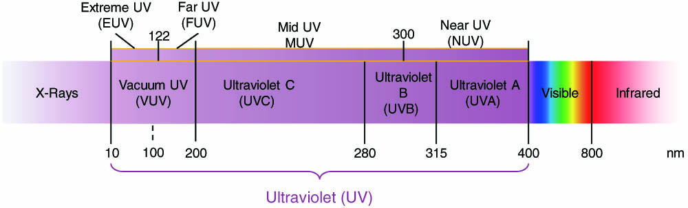
Ultraviolet (UV) detection has attracted considerable attention, owing to its versatile applications in civilian infrastructures, military facilities, and scientific research. The UV spectral region is widely established to occupy the spectral interval of and is commonly divided into the following subdivisions: near ultraviolet (NUV), mid ultraviolet (MUV), far ultraviolet (FUV), and extreme ultraviolet (EUV) [1], as shown in Fig. 1. In addition to the above names, the following names for spectral regions may be encountered: ultraviolet A (UVA), ultraviolet B (UVB), ultraviolet C (UVC), and vacuum ultraviolet (VUV) [1], where the wavelength regions are also shown in Fig. 1.
As we all know, the most important natural UV source is the Sun, which emits UV radiation at all wavelengths. However, all UVC radiation from the Sun is absorbed by the diatomic oxygen (100–200 nm) or by the ozone (triatomic oxygen) (200–280 nm) in the atmosphere. In addition, VUV light is strongly absorbed by the air. Therefore, the UV region with wavelengths of 200–280 nm is “solar blind,” meaning it can be detected without the influence of the Sun’s radiation. Detectors with a cutoff below 280 nm could be defined as solar blind because they respond only to UV radiation with wavelengths shorter than the solar radiation that can penetrate the atmosphere of the Earth. They produce no measurable signal if they are exposed to normal outdoor lighting. Solar-blind deep-UV (DUV) photodetectors with excellent thermal stability and reliability have led to various applications in monitoring ozone holes, detecting flame, space communication, missile guidance, biochemical detection, and inspection of UV leakage. One advantage of wide-bandgap (WBG) semiconductors, which include GaN (3.40 eV, bandgap energy) [2], ZnO (3.29 eV) [3], ZnS (3.76 eV) [4], ZnSe (2.82 eV) [5], SiC (2.3–3.2 eV) [6,7], AlN (6.20 eV) [8], diamond (5.5 eV) [9,10], BN (4.5–5.5 eV) [11], and gallium oxide () (4.4–5.3 eV) [12–14], and their combinations as, for example, [15], is that they can be made into solar-blind photodetectors. In addition, WBG materials are suitable for high-temperature and high-power applications [16,17] due to their high breakdown field strength in comparison to Si ( and 0.3 MV/cm [16], respectively), the most widely used semiconductor material for photodetectors (PDs).
Determined from the bandgap, binary compound semiconductors including GaN, SiC, and ZnO are mostly suitable for developing visible-blind UV detectors, which are required to have a higher responsivity in the UV range than in lower energy ranges. To meet the criteria of a solar-blind photodetector with a cutoff below 280 nm, alloying engineering to tune the bandgap up to 4.42 eV or the utilization of external Wood’s UV filters to eliminate the longer wavelength is necessary. For instance, [18] and [19] WBG ternary semiconductor alloys have been used to develop solar-blind photodetectors, and rapid progress has been achieved, including a high-performance avalanche solar-blind photodetector with improved photoresponsivity and response speed [18]. The problems lie in the epitaxial growth of alloying films with a high Al component, which requires a critical growth temperature above 1350° [20,21]. with a Mg composition over 37% will suffer phase segregation from wurtzite to rocksalt structure [22], which will introduce defects and dislocations around the separated domains and degrade the detecting performance. As one of the ultrawide-bandgap (UWBG) semiconductors, diamond material is one of the promising candidates for the development of solar-blind photodetectors [23]; however, bandgap engineering is difficult for such an elementary semiconductor [9,10], limiting its tunable photoresponse spectral range. The lack of large-area single-crystal diamond bulk material also hampers its practical application [17]. Alternatively, – is a promising candidate for solar-blind DUV detection. Monoclinic -phase has a bandgap of 4.4–4.8 eV [12] (with the corresponding wavelengths of 258–280 nm) and is expected to possess solar-blind sensitivity covering most of the range of the solar-blind UV region. Due to the availability of large-size bulk single crystals [24], homoepitaxial growth of high crystalline quality epitaxial layers with defined doping and bandgap engineering can be used to fulfill the optoelectronic potential of in UV detection [25].
Sign up for Photonics Research TOC. Get the latest issue of Photonics Research delivered right to you!Sign up now
In this review paper, we summarize recent advances in processing and device performance of solar photodetectors based on material and related heterostructures. While briefly reviewing the basic types and key parameters of photodetectors, the fundamental optical properties, and processing development of the material, the discussion mainly focuses on the device performance of photodetectors in forms of bulk, epitaxy, and nanostructures, as well as the device physics according to the architecture of photodetectors. The roles of defects and radiation damages on the transport properties and device performance are discussed as well, together with the demonstration of novel hybrid heterostructures such as avalanche solar-blind photodetectors. These advances may provide better understanding on the emerging material to fully exploit its promising optoelectronic application in the UV spectral region.
A. Basic Parameters of UV Photodetectors
1. Responsivity (Ri), Photoelectric Gain (g), and Internal Quantum Efficiency (η)
The current responsivity is one of the basic parameters to evaluate the sensitivity of a photodetector and is defined as the photocurrent per unit of incident optical power at a specific wavelength: where is the current responsivity, is the photocurrent, is the incident optical power at the specific wavelength of , is the total current under illumination, and is the dark current.
Under illumination with a specific wavelength of , the responsivity is determined by the internal quantum efficiency and the photoelectric gain , where the internal quantum efficiency is defined as the yield of carriers per incident photon and the gain is the number of carriers passing contacts per one generated pair put forth by Rose [26]. As a result, the responsivity follows the relationship where is the illumination wavelength, is the Planck’s constant, is the light velocity, is the electron charge, and is the external quantum efficiency (EQE).
2. Response Time (τ) and Bandwidth (BW)
The response speed is normally described by the response time of the photodetector. It is characterized by the decay time and rise time , as defined as the time when the photocurrent drops from 90% to 10% and rises from 10% to 90% of the maximum value, respectively. Given the decay time and the rise time, which are simply assumed to be the same, the relationship to is that . As a result, the bandwidth determined by the exponential transient response can be expressed as [27]
3. Detectivity and Noise Equivalent Power
Detectivity () for a photodetector is a figure of merit used to characterize performance, equal to the reciprocal of noise-equivalent power (NEP), normalized per square root of the sensor’s area and frequency bandwidth (reciprocal of twice the integration time), as defined to be where is the effective radiation area of detectors, is the bandwidth, and is the current noise mainly caused by carrier generation and recombination processes. There are three main contributions to the noise that limits , including dark-current-induced shot noise, Johnson–Nyquist noise, and thermal fluctuation “flicker” noise [28]. If, as expected, the shot noise from the dark current is the major contribution, the detectivity can be simplified as [28]The NEP is the optical input power for which the signal-to-noise ratio is equal to one. If the detector performance is determined by the background radiation when the thermal generation is reduced much lower than the background level, the NEP in this condition is given by [29]The NEP yields the cutoff wavelength and rejection ratio of semiconductor photodetectors. The cutoff wavelength is closely related to the bandgap energy () of the semiconductor materials.
B. Types of Photodetectors and Device Processes
UV semiconductor photodetectors can be classified into three fundamental working modes: photoconductive detectors, Schottky barrier diode (SBD), and p–n junction photodiode. Figure 2 shows the schematic structure of different semiconductor photodetectors. Since there is no sign of p-type achieved, the -based p–n homojunction has not been reported, and most -based photodetectors are working in photoconductive, SBD, or p–n heterojunctions. Herein, the basic work mechanisms of photoconductors and SBD are presented as follows.
Figure 2.Schematic structures of different semiconductor photodetectors.
The photoconductive detector (photoconductor) is essentially a radiation-sensitive resistor, which follows the basic properties of a resistor. Assuming the photoconductor has an area of and a thickness of , and if, in most conditions, the sample resistance is much larger than the contact resistance, the basic expression describing photoconductivity under equilibrium excitation can be simplified as ϕwhere is the short-circuit photocurrent under DC conditions and ϕ is the photon flux density. Under bias, the total current component caused by photon-generated electron–hole pairs is where () is the electron (hole) mobility, and () is the excess electron (hole) concentration induced by illumination, respectively.
If the change in conductivity upon irradiation is relatively small with respect to the dark conductivity by assuming uniform and complete light absorption, the voltage responsivity of an n-type semiconductor photoconductive detector can be expressed as [30]ϕwhere is the excess carrier lifetime, is the thermal equilibrium carrier concentration, and the product of ϕAhν represents the absorbed monochromatic power. From the expression of , high quantum efficiency , long excess carrier lifetime , high bias voltage , low thermal equilibrium carrier concentration , and the smallest possible piece of crystal are desirable for achieving high photoconductive responsivity under a given wavelength . When the excitation light is frequency modulated, the responsivity as a function of frequency is expressed as [30,31]where is the effective carrier lifetime, and is the excitation modulation frequency. As a result, the carrier lifetime or the response time can be fitted by the dependence of responsivity on modulation frequency [31].
2. Schottky Barrier Photodiodes
Photodiodes based on the Schottky junction, p–n junction, and type-II isotype heterojunctions, in which a built-in electric field occurs, are working in the photovoltaic mode. The built-in electric field helps separate photon-generated electron–hole pairs and excitons to move in opposite directions, which makes photodetectors exhibit self-powered properties under zero bias. In addition, the carrier transport also depends on the external circuit. In general, the Schottky barrier photodiode is a “majority carrier” device, which has unique advantages over the p–n junction dominated by minority carriers, such as simplified fabrication processes, short reverse recovery times, and high response speeds.
In terms of the ideal Schottky–Mott model [32], the rectifying property of the semiconductor and metal contact is determined by the difference in work functions of the metal () and semiconductor (). As shown in Fig. 3, for an n-type semiconductor, if , a Schottky contact forms with a barrier height given by , where is the electron affinity of the semiconductor. On the semiconductor side, is the built-in potential barrier, expressed as , which is slightly dependent on the Fermi level of the semiconductor determined by the doping level. However, the built-in barrier of a real Schottky diode does not follow such an ideal and simple relationship with for a given semiconductor practically, as it is effectively reduced owing to the imaging force [33,34] and the presence of interface states [35]. Therefore, there are numerous and considerable variations among experimental data on and , which will be discussed in the following section by focusing on the fabrication processes of -based SBD photodetectors.
Figure 3.(a) Energy band diagram of a metal and a semiconductor before contact; (b) ideal energy band diagram of a metal/n–semiconductor junction for .
Various theories [36–39] have been developed to describe the carrier transport over the energy barrier of the Schottky diode. Among these theories, the thermal emission theory appears to explain the current–voltage (I–V) properties of high-mobility semiconductors [37], and the thermionic diffusion theory is applicable to low-mobility semiconductors [40]. In the presence of interfacial defects, the trap-assisted tunneling [41] and hopping [42] conduction mechanisms may also dominate the transport properties. In terms of thermionic theory, the current density of electrons for n-type semiconductors transported from the semiconductor over the potential barrier into the metal in the dark condition is expressed as [39]where is the external applied voltage, is the ideality factor, is the Boltzmann’s constant, is the temperature, is the saturation current density as expressed as , is the Richardson constant, and is the effective electron mass. From Eq. (11), the saturation current density is very sensitive to temperature. The current density expressions of the thermionic diffusion and the thermionic emission theories are very similar except the expression of the saturation current density. The saturation current density in the diffusion theory is expressed as [30]where is the diffusion coefficient, is the density of states in the conduction band, and is the donor density. As compared to the thermionic theory, the saturation current density in the framework of the thermionic diffusion mechanism is less sensitive to temperature variation.
For a nondegenerated n-type semiconductor, the contribution of light illumination to the current is primarily due to photogenerated carriers in the depletion region, with a width of [32]. Thus, the photocurrent density under a single-photon flux density ϕ, which flows in the negative direction, depends on the applied voltage given by ϕ[43], and is the absorption coefficient of the material. Consequently, the current responsivity can be obtained through the relationship of ϕ. However, the existence of trapping states () at the Schottky contact interface, which originate from the surface states, metal-induced gap states, and/or the interface chemical reactions of metal and semiconductor atoms, will trap the photogenerated holes in the topmost surface region of the semiconductor side and generates net positive charges of [43]. Under illumination, photogenerated holes drift towards the surface region and are trapped by these traps, which produces net positive charge . The metal negative charges and the positive charges in the depletion region satisfy the neutrality condition of . As a result, under an illumination circumstance, the amount of the band-bending will be reduced in terms of the relationship of [43,44], where is the barrier height in the dark condition, and is the width of the depletion region. The decrease in under illumination will reduce the Schottky barrier , denoted as . The reduction of is determined by the trapping states and the external applied voltage, leading to the reduction of the Schottky barrier. Accounting for the current contribution by the reduction of the Schottky barrier and by photogenerated excess carriers, the entire current under illumination is where the photocurrent component is contributed by the photon-generated electron–hole pairs in the depletion layer and has the opposite current direction against the dark current component and no contribution to the photoconductive gain. As a result, the responsivity can be expressed as [43,44]Hence, the responsivity will differ under different light intensity below the saturation light intensity and the applied voltage. In the presence of traps, there are two mechanisms responsible for the observed photoresponse, including the component maintained by photogenerated excess carriers in the depletion region and the lowering effect of the Schottky barrier caused by trapping of photogenerated holes near the surface [43]. In fact, photogenerated holes localized at the trapping states at the metal−semiconductor interface will lead to high photoconductive gain but low response speed, which is commonly observed in the most -based solar-blind photodetectors, as discussed later on. The yield of huge high gain is caused by longer trapping and detrapping times as compared with the transit time of the electrons between the contacts and the resistive-capacitive (RC) delay time of the circuit.
3. Ohmic Contacts
Ohmic and Schottky contacts are essential for high-performance, high-reliability, and high-efficiency -based UV photodetectors. Ohmic contacts can be applied in both photoconductors and Schottky barrier photodetectors while Schottky contacts are the basis of self-powered Schottky barrier photodetectors.
To avoid reducing device switching speeds and encountering the reliability issues due to local contact heating during device operation, additional contact resistance should be excluded. According to the ideal Schottky–Mott model, for an n-type semiconductor, to achieve an Ohmic contact means that the work function of the metal should be equal to or smaller than that of the host semiconductor material. Since the work function of a practical-interest n-type semiconductor is mainly determined by the affinity of the semiconductor material, to achieve Ohmic contacts to , the work function of the metal should be close to or smaller than the affinity of , which is reported to be [33]. Therefore, Hf (3.9 eV, work function), Sc and La (both 3.5 eV), Zn (3.63 eV), and Gd (2.90 eV) are the potential choices for Ohmic contacts to [45]. Most likely the contact will be bilayers of these with Au to reduce the contact sheet resistance and improve their reliability. A basic physical parameter used to describe the contact properties is the specific contact resistance , which is independent of the contact geometry compared to the contact resistance and is typically expressed in the unit of . The transport properties in the contacts including the contact resistance , the specific contact resistance , the transfer length , and the resistance of the semiconductor can be determined by the temperature-dependent transmission line method (TLM) or circular TLM (CTLM) measurements.
However, for UWBG semiconductors, Ohmic contact is a critical issue as commonly used metals have large work function and large barrier heights exist in the interface of semiconductors and metals [46]. The carrier transport properties and the specific contact resistance are mainly determined by the Schottky barrier and the doping concentration of the semiconductor. When the n-type semiconductor is nondegenerated with a doping concentration of about , the thermionic field emission is operative, and the specific constant resistance can be calculated from To realize the reduction of the barrier height or the depletion width, heavier doping processes by in situ doping [47] or implantation [48–50] have been widely employed, which enhance the tunneling of electrons by reducing the barrier width. As is degenerated, the specific contact resistance follows the relationship of [32]Table 1 shows a summary of Ohmic contact processes to from the reported literature. Specific contact resistance with optimal values in the range of was achieved after processes of Si implantation, surface treatment, Ti-based metal stack, and rapid thermal annealing (RTA) [48,51–59]. In particular, degenerate doping in the selective region of by Si implantation and postannealing activation in a temperature range of about 950°C are employed to realize electron tunneling and a rather low specific on-resistance [48,51]. Besides, In- and Ti-based electrodes are often utilized to form Ohmic contacts. However, In is properly not optimal due to the low melting point of only 157°C, while Ti contacts will be degraded above 600°C due to oxidation reactions with [60]. Therefore, the RTA process for the electrode based on Ti has an optimized temperature of about 470°C [51,52,54–57]. Metal stacks with an adherent layer of Ti, an overlayer of Al, a barrier layer of Ni, and a cap layer of Au are used to reduce the sheet resistance of the contact. Metal bilayers of Ti/Au, and post-treatment of thermal annealing have also been attempted in the formation of Ohmic contacts to . Surface pretreatment with plasma exposure, reactive ion etching, and ion implantation is another alternative approach to reduce the barrier height by introducing a large amount of surface defects or increasing the effective shallow donor concentration on the surface by preferential loss of oxygen [52,53,55–58]. Intermediate semiconductors such as ITO [61,62] or ZnO [59] with a lower bandgap have also been employed to reduce the conduction band offset and improve carrier transport at the interface. It was reported that ITO/Pt contacts on showed much better Ohmic contact than Ti/Pt contacts, which was attributed to the formation of a lower bandgap intermediate semiconductor layer and a higher doping concentration than the unintentionally doped (UID) [62].
Metal Stack
Doping (cm−3)
Treatments
ρc (Ω · cm2)/Method
Reference
Ti/Au (50/300 nm)
3×10¹⁹
Si implantation in contact region 950°C annealing for implant activation 450 °C RTA for contact
4.6×10⁻⁶/CTLM
Sasaki et al. [48]
Ti/Au
5×10¹⁹
Si implantation in contact region 925°C annealing for implant activation 470°C RTA for contact
4.6×10⁻⁶/CTLM
Higashiwaki et al. [51]
Ti/Au (20/230 nm)
3×10¹⁹
Si implantation in contact region 950°C annealing for implant activation BCl3 ICP etching prior 470°C RTA for contact
7.5×10⁻⁶/TLM
Wong et al. [52]
Ti/Au
3×10¹⁸
diffusion of Sn from the SOG layer BCl3/Ar ICP etching prior 450°C RTA for contact
(2.1±1.4)×10−5/TLM
Zeng et al. [53]
Ti/Au (30/130 nm)
1020
degenerately doped contact layer with a high Si doping concentration above 1020cm−3 470°C RTA for contact
1.1Ω·mm/TLM
Zhang et al. [54]
Ti/Au/Ni
2.4×1014cm−2
BCl3 ICP/RIE etching prior 470°C RTA for contact
4.6×10⁻⁶/TLM
Krishnamoorthy et al. [55]
Ti/Al/Au (15/60/50 nm)
2.7×10¹⁸
Ar plasma treatment
2.7Ω·mm/TLM
Zhou et al. [63]
Ti/Al/Ni/Au
∼1019
BCl3 ICP etching prior 470°C RTA for contact
4.7Ω·mm/TLM
Chabak et al. [56]
Ti/Al/Ni/Au (20/100/50/50 nm)
4.8×10¹⁷
BCl3 ICP/RIE etching prior 470°C RTA for contact
16Ω·mm/CTLM
Green et al. [57]
Ti/Al/Ni/Au
∼1018
BCl3 ICP etching prior
10.7–80.0Ω·mm/CTLM
Moser et al. [58]
AZO/Ti/Au (10/20/80 nm)
∼1019 [48]
Si implantation in contact region 950°C annealing for implant activation 400°C RTA for contact
2.82×10⁻⁵/TLM
Carey et al. [59]
ITO/Ti/Au (10/20/80 nm)
∼1019 [48]
Si implantation in contact region 950°C annealing for implant activation 600°C RTA for contact
6.3×10⁻⁵/TLM
Carey et al. [61]
ITO/Pt (140/100 nm)
2×10¹⁷
800–1200°C RTA for contact
not measured but Ohmic for annealing above 900°C
Zhou et al. [62]
Ti, In, Ag, Sn, W, Mo, Sc, Zn, and Zr (20 nm), with Au (100 nm) overlayers
5×10¹⁸
400–800°C RTA for contact
not measuredIn and Ti produced linear I–V curves after anneals
For the -based Schottky diodes, the nonideal factors including the presence of interface-induced subgap states [33,64], the upward band-bending effect [34,64–66], and the Schottky barrier lowering due to the nonequilibrium carrier often affect the barrier height [43,67]. Table 2 demonstrates that the reported values of Schottky barrier height (SBH) and ideality factor , are varied with the n-type doping concentration and processes of different metals for Schottky contacts to . As is well known, the barrier height can be extracted from the linear portions of the I–V curve and the voltage intercept in the forward bias region from the – curve, respectively. However, the I–V determined values, which are lower than those determined by the C–V method [64,68–70], should be more representative to the effective SBHs for current flow. As shown in Table 2, regardless of the metal used, the typical barrier heights are in the range of 1.00–1.50 eV when the ideality factor is close to 1. The large ideality factor () is due to the generation recombination in the depletion region, tunneling, and/or terminal edge leakage [71], which may degrade the Schottky device performance and affect the detecting properties under illumination.
Metal
Barrier Height (eV)
Ideality Factor
Doping (cm−3)
Process/Measurement
Comments
Reference
Ni
1.25
1.01
∼1.13×10¹⁷
evaporation Ni/Au, I–V and C–V
built-in voltage is 1.18 V from C–V and 1.0 V from I–V
Oishi et al. [68]
Ni
1.05
not measured
1.7×10¹⁷
DC–sputtering, I–V and C–V
higher barrier measured with C–V
Armstrong et al. [69]
Ni
1.08–1.12
1.05–1.10
(1.0–2.5)×1017
evaporation Ni/Au, I–V
sample etched with H3PO4 at 140°C
Kasu et al. [74]
Ni
0.95
3.38
UID
e-beam deposition Ni/Au, I–V
barrier height increase, and ideality factor decrease with temperature
Oh et al. [75]
Ni
0.8–1.0
1.8–3.2
UID
evaporation, I–V
(AlxGa1−x)2O3 with x up to 0.164
Ahmadi et al. [71]
Ni
1.07
1.3
∼9×10¹⁶
e-beam deposition Ni/Au, I–V
barrier height increase, and ideality factor decrease with temperature
Ahn et al. [76]
Ni
1.54
1.04
∼1.1×10¹⁷
e-beam deposition, I–V
similar value to that from C–V
Farzana et al. [77]
Ni
1.10
1.05
∼2.8×10¹⁷
evaporation Ni/Au, I–V and C–V
sample etched with H3PO4 at 140°C
Kasu et al. [78]
Ni
1.2
1.00
∼3×10¹⁷
e-beam deposition Ni/Au, I–V
dry etch damage to Schottky contact
Yang et al. [79]
Ni
0.99–1.02
1.05–1.09
∼3×10¹⁷
evaporation Ni/Au, I–V
(001) substrate
Oshima et al. [80]
Ni
1.04±0.021.08±0.11.00±0.06
1.33±0.031.68±0.041.57±0.2
(5–8)×1018 UID (5–8)×1018
e-beam evaporation, I–V
cleaned with HCl and H2O2, vertical SBD
Yao et al. [72]
Ni
0.81
2.29
UID
I–V
(AlxGa1−x)2O3 with x to about 0.08
Qian et al. [81]
Pt
1.35–1.52
1.04–1.06
(0.3–1)×1017
evaporation Pt/Ti/Au, I–V and C–V
sample etched with 85 wt.% H3PO4 at 135°C, higher barrier measured with C–V
Sasaki et al. [70]
Pt
1.15
∼1.0
∼1.0×10¹⁶
evaporation Pt/Ti/Au, I–V and C–V
A* was calculated to be 55A·cm−2·K−2
Higashiwaki et al. [82]
Pt
1.04
1.28
∼9×10¹⁶
e-beam deposition Pt/Au, I–V
barrier height increase, and ideality factor decrease with temperature
Ahn et al. [76]
Pt
1.58
1.03
∼1.1×10¹⁷
e-beam deposition, I–V
similar value to that from C–V
Farzana et al. [77]
Pt
1.39
1.1
2.3×10¹⁴
sputtering Pt/Ti/Au, I–V
barrier height stable up to at least 150°C
He et al. [83]
Pt
1.46
1.03±0.02
1.8×10¹⁶
evaporation Pt/Ti/Au, I–V and C–V
barrier height may be increasing by the presence of F
Konishi et al. [84]
Pt
1.01
1.07
∼3×10¹⁷
e-beam evaporation Pt/Au, I–V
comparison to TiN
Tadjer et al. [73]
Pt
1.05±0.031.34±0.1
1.40±0.041.87±0.3
(5–8)×1018 UID
e-beam evaporation, I–V
bulk and epilayer SBD, cleaned with HCl and H2O2
Yao et al. [72]
Pt
1.05–1.20
1.34–1.55
∼4.2×10¹⁸
e-beam evaporation Pt/Au, I–V
both (010) and (2¯01) single-crystal substrates were used; the (010) SBD had a larger VON
Fu et al. [64]
Au
1.07
1.02
(0.6–8)×1017
e-beam deposition, I–V
affinity of Ga2O34.00±0.05eV, work function of Au 5.23±0.05eV
Mohamed et al. [33]
Au
1.71
1.09
∼1.1×10¹⁷
e-beam deposition, I–V
interface consistent with inhomogeneous barrier
Farzana et al. [77]
Au
∼1.1
1.08
1017–1018
e-beam deposition, I–V
barrier height decrease, and ideality factor decrease to near unity after annealing at temperature above 200°C
Suzuki et al. [85]
Pd
1.27
1.05
∼1.1×10¹⁷
e-beam deposition, I–V
similar value to that from C–V
Farzana et al. [77]
Cu
1.32
1.03
1.6×10¹⁸
DC sputtering, I–V
low-mobility Ga2O3 layer grown by PLD
Splith et al. [86]
Cu
0.98, 1.07
1.05, 1.1
6×10¹⁶
Cu/Au/Ni, I–V
SBD, MOSSBD
Sasaki et al. [87]
Cu
1.13±0.1
1.53±0.2
(5–8)×1018
e-beam evaporation, I–V
bulk vertical SBD, cleaned with HCl and H2O2
Yao et al. [72]
W
0.91±0.091.05±0.03
1.40±0.42.68±0.3
(5–8)×1018 UID
e-beam evaporation, I–V
bulk and epilayer SBD, cleaned with HCl and H2O2
Yao et al. [72]
Ir
1.29±0.1
1.45±0.2
(5–8)×1018 UID
e-beam evaporation, I–V
bulk and epilayer SBD, cleaned with HCl and H2O2
Yao et al. [72]
TiN
0.98
1.09
∼3×10¹⁷
ALD 350°C, I–V
similar to Pt used as comparison
Tadjer et al. [73]
PtOx
1.94
1.09
1017
magnetron sputtering PtOx/Pt, I–V
bulk crystal
Müller et al. [34]
1.42
1.28
(0.5–1)×1018
PLD sample
Table 2. Summary of Reported Schottky Barrier Contacts to
Figure 4 shows the summary of the SBH as a function of metals with different work functions. The short dashed curve represents the ideal SBH based on the ideal Schottky–Mott model, where the electron affinity of the is chosen to be 4.00 eV [33]. It is found that the values of SBH determined by the I–V or C–V are scattered and show a weak correlation with the work functions of the metals. Comparing the reported SBH with the ideal Schottky–Mott model, the factors other than the metal work function should be taken into account to evaluate the Schottky barrier in . For instance, the method of metal deposition also plays an important role in determining the effective barrier. The barrier height of the same metal also varies on with different orientation, which could result from the different surface reconstruction and different surface state density [64,72]. Besides metals, highly conductive metal-like nitrides and oxides can also be employed to form the Schottky contact [34,73]. Tadjer et al.[73] and Müller et al.[34] have proven that TiN deposited by ALD and deposited by sputtering are good replacement materials to form the Schottky contact to .
Figure 4.Dependence of the Schottky barrier height on the metal work function of different metals, and the ideal Schottky barrier height based on the Schottky–Mott model (short dashed curve).
As one of the representative UBG semiconductor materials, has a WBG of about 4.4–5.3 eV [12–14], which corresponds to the wavelength at the UVC spectral region. The variation of the bandgap results from the different polymorphs of with different structure symmetry [13,88–91] and its anisotropy along different orientations [12,89,92]. has six different phases, among which the -phase is the most thermodynamically stable phase [93], and most studies have been focused on in the last decade. The most stable has monoclinic structure, which belongs to space group [94,95]. Any other polymorphs of will be transformed to -phase at sufficiently high temperature in air atmosphere [93,96], as shown in Fig. 5. Table 3 is a summary of the basic parameters of different phases of . The bandgap of the is reported to be varied from 4.4 to 5.0 eV, determined by the optical transitions from the valence band maximum (VBM) to the conduction band minimum (CBM) according to the polarization golden rules [12].
Figure 5.Chart illustrating transformation relationships among the forms of and its hydrates. Redraw with permission from Roy et al. [93]. Copyright 1952 American Chemical Society.
The other five polymorphs are commonly identified as -, -, -, -, and -, which are less studied, but recently have drawn increasing attention due to their interesting properties. The metastable polymorph has a rhombohedral structure, analogous to corundum (sapphire, ) with the space group of [97,98]. The bandgap of is reported to be about 5.3 eV [13,14,91], which means that it can be used in solar-blind detectors with a shorter cutoff wavelength and a higher breakdown electric field than the commonly used material. is thermodynamically a semistable phase and initially can only be synthesized at high pressures [14]. By strain engineering, Fujita et al.[14] reported the growth of high quality thin films on sapphire substrates under atmospheric pressure at a temperature lower than 500°C [91]. The phase transition temperature of can be lifted up to about 800°C when an alloying buffer layer is introduced [99]. In addition, , along with other corundum-structured III-oxide semiconductors, and , enables the design and delivery of high-performance WBG heterostructure devices [14], such UV detectors with a wider sensitive range, Schottky diodes with a higher breakdown voltage, and high electron mobility transistors (HEMTs) based on modulation-doped [54,100].
The has a defective cubic spinel-type structure (-type) with a space group of [101–103], and its bandgap was reported to be 5.0 eV (direct bandgap) or 4.4 eV (indirect bandgap), whereas the specific band structure and the nature of optical transition in are still under a lack of study [102]. The other two polymorphs, and , were first synthesized by Roy et al.[93] in 1952. The structure of was assumed to be structurally related to cubic defect spinels, such as , , and other oxides [96]. Recent research indicates that pure thin films exhibit ferroelectric properties with strong spontaneous polarization [104,105]. The space group of was tentatively assigned as [96,104,106], analogous to hexagonal GaN and ZnO materials, while the density functional theory (DFT) calculation and recent experimental results identify in the orthorhombic symmetry [98,107,108], which is as an ordered subgroup of the hexagonal [108,109]. The direct bandgap of is determined to be 4.9 eV from the plot by Oshima et al.[106], while Nishinaka et al.[110] evaluated the optical bandgap of from the direct transition to be 5.0 eV and from the indirect transition to be 4.5 eV, respectively. Pure-phase high-quality thin films can be heteroepitaxially grown on the inexpensive substrates, including sapphire, [107,111], SiC [112], GaN [106], AlN [106], and MgO [110], which indicates provides more opportunities to design the optoelectronic devices by combining with other WBG semiconductors. Nevertheless, due to the most thermodynamically stable phase and the availability of single crystalline substrate, most of the reported solar-blind photodetectors and power electronic devices are developed based on -phase . Therefore, the following sections will mainly focus on the discussion of the band structure of and the synthesis of materials in various forms of bulk, thin film, and nanostructures.
A. Bulk Crystal and Epitaxial Films of Ga2O3
Among the polymorphs of , is the only one that is stable until the melting point under an atmospheric pressure of about 1800°C [114]. Various melt growth methods, including the Verneuil method [115,116], Vertical Bridgman [117,118], floating zone (FZ) process [119–130], Czochralski process (CZ) [114,131–133], and edge-defined film-fed growth (EFG) process [24,134–136], have been reported to synthesize the bulk materials. Flux [137–139] and gas [140–142] phase methods have also been demonstrated for the growth of , but the crystal size is too small for practical applications. Most of the UID bulk single crystal exhibits n-type conductivity, which is possibly a result of intrinsic shallow donor defects (Ga interstitial) [143] or external impurities (H, C or Si) [24,130]. Similar to the asymmetric doping in ZnO, n-type conductivity of single crystals or epitaxial films can be easily achieved by the doping of tetravalent elements (Si, Sn, or Ge) with a resultant free-electron concentration in the range of –[24,25,128,143–150]. In contrast, no effective p-type conductivity of has been reported, which is strongly hindered by a very low formation energy of self-trapped holes (STHs) [69,151,152] and almost no dispersion of the energy levels near the top of the valence band [153,154]. Doping with Fe, Mg, and N does not convert into p-type but results in the semi-insulating status [154–157], which has been used as substrates for the fabrication of MOSFET devices with low leakage current [49,57,100,158].
To date, large-size bulk crystals were mainly synthesized at a growth rate up to 10 mm/h by using the EFG technique [24], which has been widely used to produce large-size sapphire bulk material. The 2 inch (1 inch = 2.54 cm) UID and Fe-doped semi-insulating wafers with orientations of and (100) are commercially available, and 6 inch technology is also under development [24]. The major residual donor impurities in the UID crystal are Si with its concentration of about , which is consistent with the C–V measurements of an () value of 2 . Therefore, UID bulk crystals have a typical electron background concentration in the level and an electron mobility of at room temperature [68,131,143,159]. The in situ doping of Sn or Si can be achieved with the carrier concentration in the range of to [24]. Since the crystallographic direction is parallel to both the cleavage planes and [160], the (100)- and (001)-oriented substrates are fragile during the fabrication processes [24]. Interestingly, a large lattice constant along the [100] direction facilitates the mechanical cleavage of the crystal into thin flakes or nanomembranes [161] along this plane, which provides an alternative platform to develop membrane-based field-effect transistors (FETs) [63,161–166] and solar-blind photodetectors [167–170].
To meet the high demand for power electronic device applications, great efforts have been made on the epitaxial growth of thin films in recent years by various technological means, including molecular beam epitaxy (MBE) [25,171,172], metal–organic vapor phase epitaxy (MOVPE) [145,173], halide vapor phase epitaxy (HVPE) [174,175], low-pressure chemical vapor deposition (LPCVD) [176,177], pulsed laser deposition (PLD) [90,148], and mist chemical vapor deposition (mist-CVD) [146]. Due to the availability of bulk substrates, high-quality homoepitaxy of , and the related ternary alloying films with low densities of dislocation and defects, a well-controlled n-type doping by Si, a high electron mobility, and an atomic smooth surface morphology, have been achieved [25,145,147,178]. High-crystalline-quality heterostructures have been produced by plasma-assisted MBE with modulation doping of Si [100,178] and Ge [179] and high-mobility 2D electron gas has been observed at their interface, which delivers the demonstration of the first HEMT based on [100]. However, the crystalline quality of the heteroepitaxial growth of thin films (mainly on -plane sapphire) is poor. The crystalline structure difference and lattice misfit between and lead to 3D island growth, lattice twist, and phase segregation at the interface [180]. In addition, it is very difficult to realize the defined doping in these heteroepitaxially-grown films.
In contrast, the other metastable polymorphs, including -, , and thin films, have been heteroepitaxially grown on foreign substrates including sapphire, AlN [106], SiC [112], GaN [106], ZnO [181], and MgO [110]. The used epitaxial techniques are mostly based on chemical vapor deposition (CVD) techniques, such as mist-CVD, HVPE, and MOCVD. For instance, high-crystalline-quality thin films with device-acceptable doping and the ternary epilayers have been grown on sapphire substrates using the mist-CVD technique developed by Fujita et al.[182–184]. The films on sapphire exhibit a narrow diffraction peak for the (0006) plane with typical FWHMs of 30–60 arcsec [184]. Recently, the highest mobility of was achieved for the Si-doped film at the carrier density of [185]. With advances of the mist-CVD technique in low-temperature synthesis, high growth rate, well-controlled doping and low-cost, high-voltage Schottky rectifiers [186] and metal-semiconductor-field-effect-transistors (MESFETs) [187] based on have been demonstrated, which are even superior to the devices based on the homoepilayers. In addition, a pure-phase can also be grown by MBE [107] and PLD [188] on sapphire, but the optimized growth window is quite narrow because of the formation of mixed - and -phases as compared to the CVD methods. Having similar hexagonal symmetry with common WBG semiconductors, is normally achieved on sapphire, GaN, AlN, and SiC substrates, and unique properties such as ferroelectric polarization have been discovered [104,105]. However, the crystalline quality is still fair due to the domain rotation with respect to the substrates. If the material quality meets the criteria of device fabrication, it is expected that will provide an alternative platform for the development of low-consumption transistors, switchable memories, and UV photodetectors. A few studies have reported the epitaxial growth of thin films [102,189], but the fundamental properties of thin films are rare.
B. Nanostructures of β-Ga2O3
Low-dimensional crystalline nanostructures in a variety of forms, such as nanocrystals [190–196], nanowires (NWs) [197–241], nanorods (NRs) [242–251], nanobelts (NBs) [248,249,252–256], nanosheets (NSHs) [248,249,252,257–259], and other configured structures [220–222,224,260–263], have been synthesized by various means, as summarized in Fig. 6. NBs or nanoflakes of can also be produced from the (100) single crystal substrate by a mechanical exfoliation method [163,167–170,264,265]. These low-dimensional structures have been utilized in the investigation of the fundamental properties as well as the implementation of functional devices including FETs [163,202], gas sensors [197,209,225], and solar-blind photodetectors [207,254,266].
Figure 6.Various nanostructures. (a) nanocrystals. Reprinted with permission from Wang et al. [196]. Copyright 2010 American Chemical Society. (b) nanowires. Reprinted with permission from Nogales et al. [229]. Copyright 2007 American Institute of Physics. (c) shell@core NWs. Reprinted with permission from Lupan et al. [234]. Copyright 2015 Elsevier B.V. (d) nanorods. Reprinted with permission from Vanithakumari et al. [244]. Copyright 2009 Wiley-VCH Verlag GmbH & Co. KGaA, Weinheim. (e) As-synthesized nanobelt. Reprinted with permission from Zou et al. [256]. Copyright 2014 Wiley-VCH Verlag GmbH & Co. KGaA, Weinheim. (f) Branched multiwire nanostructures (left) and its X-ray fluorescence (XRF) map (right). Reprinted with permission from Martinez-Criado et al. [224]. Copyright 2014 American Chemical Society.
Several approaches have been developed to synthesize nanostructures, such as the vapor–liquid–solid (VLS) or vapor–solid (VS) process [206,213,220,267], the solution process [190,196,255,268], physical evaporation [203,224,235,248], plasma exposure [257], thermal oxidation of compacted gallium nitride powder [249,269], and thermal reduction chemical vapor transport (CVT) [256], as well as recently developed mechanical exfoliation methods. The VLS and VS processes have been proven to be favorable to achieve high-quality nanostructures, especially NWs [270]. In the VLS process, Au is the most commonly used metal catalyst to grow nanostructures. Terasako et al.[233] reported that the average diameter of NWs and the morphology of nanostructures, such as NWs, NBs, and NSHs, can be controlled by tuning the Au thickness, the growth time, and the growth temperature. Alternatively, Johnson et al.[212] reported the use of Fe as the catalyst to grow GaN NWs, NWs, and nanoribbons by using ion implantation of into the thermally grown layers and subsequent annealing to form the catalyst nanoparticles. However, the use of a metal catalyst has the risk of some level of impurity incorporation into the , which may introduce deep-level defects and affect the electrical properties of the material. Cho et al.[248] investigated that various forms of nanostructures such as NWs, NRs, NBs, NSHs, and nanocolumns could be successfully synthesized by simple evaporation of metallic gallium with no assisted catalyst in a flow of argon gas. Zhao et al.[240,271] reported – core–shell microwires synthesized using a one-step approach on Si substrate by the CVD method. Because of the different growth threshold temperature of ZnO (900°C) and (1100°C), the synthesis of the – core–shell structure could be designed in one temperature rise continuous reaction process [271]. The ZnO core and the shell were both single crystalline with few noticeable structural defects at the interface, which enables the demonstration of -based APDs.
In addition, several dopants such as N [201,250], Zn [202], Li [220], Cr [221,222,228,229,245], Sn[222,226], Er [229,261], and In [237] have been reported to be doped in nanostructures and predominantly modify the optical properties. The presence of Sn leads to a broad emission in the UV-blue and UV-green ranges as observed by cathodoluminescence (CL) characterizations [222]. Lithium is of potential interest as a dopant in nanostructures to modify its conductivity for electrical energy storage applications. However, no evidence proves the difference in conductivity of the nanostructures with Li doping [220]. Zinc was expected to be a shallow acceptor by a diffusive doping method to increase the mobile carriers in NWs [202] with a demonstration of p-channel FETs. However, it is still debatable due to a low hole mobility of . Despite distinguished advantages of nanostructure-based devices, the reproducibility of the nanostructures and realization of high-yield and high-reliability contacts remain challenging issues. Effective doping to control the electrical and optical properties of nanostructures is also complicated, which hampers their practical applications.
C. Band Structures of β-Ga2O3
is the most representative in the polymorphs of , and its band structure has been investigated considerably in theoretical and experimental aspects. Figure 7 displays the schematic structure of a unit cell. As mentioned above, has a monoclinic structure, where the angle . The unit cell of contains two crystallographically different Ga atoms in the asymmetric unit, one with tetrahedral () and the other with octahedral () coordination geometry. Correspondingly, there are three types of oxygen ions () in the unit cell, which leads to an anisotropy in thermal conductivities [272], phonon vibrational modes [273], effective mass [89,274], optical bandgap [12,89,275], and surface formation energy [276,277]. For instance, the optical anisotropy of is caused by the transitions of electrons from the valence bands to the CBM according to the Fermi golden selection rules [12].
Figure 7.The crystal structure of and its surfaces.
The band structure of calculated by DFT is shown in Fig. 8[275]. The CBM is located at the point (the Brillouin zone center) and is isotropic with the effective electron mass in the range of 0.24–0.34[95,278,279]. The VBM is located at the point (½, ½, ½), while in most previous publications it is labeled as the point [275]. The VBM is slightly higher than (less than 100 meV) as reported by theoretical calculation and experimental results [12,92,95,274,275,279,280], which strongly suggests that is an indirect bandgap semiconductor. The indirect bandgap is slightly smaller than the direct bandgap with the energy difference of 0.03–0.04 eV by Onuma et al.[12]. The calculated results are in good agreement with absorption [12] and angle-resolved photoemission spectroscopy (ARPES) measurements [280–282]. Recently, the indirect nature of optical transition is identified to be retained after alloying with Al, and the VBM eigenvalue differences between the and points become larger as the Al content increases in [283]. The indirect bandgap nature of is as expected when one considers the fact that the top valence band is predominantly formed by orbitals. As has been proven to be an indirect semiconductor, the typical emission spectra recorded by means of photoluminescence (PL) and CL do not exhibit near-band-edge (NBE) emissions corresponding to the band-to-band optical transitions, while the UV luminescence (UVL) and blue luminescence (BL) bands related to the intrinsic defects are widely observed in with various forms of bulk, epilayers, or nanostructures [155,284,285]. The UVL band is widely recognized as being impurity independent [285,286], and experimental [285,286] and theoretical [151] studies have attributed it to the recombination of free electrons and STHs or self-trapped excitons. The BL band has been attributed to the donor–acceptor pair transitions involving deep donors and acceptors [286,287]. Therefore, although the detector based on is insensitive to the light it emits, the subgap absorption via these intrinsic defects will definitely reduce the UVC-to-UVA rejection ratio of the photoresponsivity and degrade the performance of the solar-blind detection. The existence of subgap defects is also an origin to produce a persistent photoconductivity (PPC) effect, which hinders the high-speed operation of the photodiodes for practical applications. Therefore, the suppression of defect-related subgap absorption is critical, and improving material growth technologies is the key solution to achieve low-defect density and high performance of the final devices.
Figure 8.Band structure of . (a) At the GGA–DFT (PBE) level and (b) at the hybrid HF–DFT (Gau–PBE) level. Reprinted with permission from Mock et al. [275]. Copyright 2017 American Physical Society.
In addition, the valence band ordering in contributes to the various transition from the valence bands to the CBM. The variation in band-to-band transition determines the absorption edges observed in experiments without taking the Urbach tail states into account. Polarized reflectance spectra and transmission spectra of different-orientation single-crystalline substrates can be used to determine the energies of different transitions from VBM to the CBM in terms of the selection rules. The polarized absorption edges are located at 4.48 eV, 4.57 eV, and 4.70 eV with incident light having the configuration of , (or , where the axis is perpendicular to the (100) plane and is angled at from the axis), and , respectively, at room temperature (RT). Therefore, the unpolarized transmittance spectra from the substrates must exhibit a distinct shoulder at 4.5–4.7 eV [12,89], and correspondingly, the shoulder will affect the responsivity of solar-blind photodetectors. The variation in reflectance and the absorption edges of different-orientation bulk crystals are shown in Fig. 9[12]. Accordingly, the spectral wavelength of peak photoresponsivity of -based photodetectors would be sensitive to the polarization of the incident light. From the viewpoint of reliability, the polarization-dependent photoresponsivity is indeed an undesirable trait for practical photodetectors. To minimize the effect of optical anisotropy on the responsivity of the devices, it would be better to choose (010) oriented crystals, which demonstrate a minimum difference on absorption edges of only . Furthermore, the optical anisotropic characteristics are almost negligible in epitaxial layers, which would also be a good solution to this problem. On the other hand, the polarization-sensitive anisotropic absorption may also open an opportunity to develop spectrally selective solar-blind photodetectors by light polarization engineering in single crystals. For example, similar to the bandpass photodetectors based on nonpolar GaN and ZnO epilayers, by combining an identical (100) single crystal with an orthogonal alignment to the planar detector, a highly narrow band photodetector demonstrates the strong capability to detect weak signals of DUV light with a specific wavelength and its polarization state. It provides a new paradigm for narrow bandpass photodetectors with broad applications where noises from a full daylight background or environmental radiation need to be suppressed [288–290].
Figure 9. versus plots for (a) (010) Mg-doped substrate for (closed circles) and (open circles) at RT. (b) Data set of (001) undoped substrate for (closed squares) and (open squares). Dotted lines represent the energies of the direct absorption edge. Partially polarized reflectance spectra at RT are shown in the upper part of the figures. Energies of the dips and the shoulder are indicated by the vertical arrows. Reprinted with permission from Onuma et al. [12]. Copyright 2015 The Japan Society of Applied Physics.
It has been reported that the conductivity of could be easily tuned over many orders of magnitude ranging from to [120,155]. To further extend the utility and applications of in photodetectors as well as other bipolar optoelectronic devices, it is necessary to realize stable and reliable p-type . However, for WBG transparent oxide semiconductors, such as ZnO, , and , the creation of positive carriers (holes) is a most challenging issue, which is mainly limited by (i) the high formation energy of the native acceptors that produce holes, such as cation vacancies; and (ii) the low formation energy of native donors that compensate acceptors, such as anion vacancies [291]. The native point defects in that act as donors, which are oxygen vacancies at threefold coordinated sites (O1 and O2) and fourfold coordinated sites (O3), do not directly contribute to the electrical conductivity because of the high formation energies of 3.31, 2.7, and 3.57 eV for O1, O2, and O3, respectively [292]. On the other hand, acts as a deep-level acceptor with a large ionization energy. Therefore, intrinsic vacancies alone cannot contribute enough free carriers for the electrical conductivity of . Hydrogen as well as other external impurities such as Si, Ge, and Sn could be the contributors to the n-type conduction of unintentionally doped with a background electron concentration of to .
There are two possible types of potential dopants for effective p-type doping in : group V anions that substitute one of the oxygen sites, such as N, and group I, II, and IIB cations that substitute one of the gallium sites, such as Li, Mg, and Zn. Kyrtsos et al.[153] theoretically investigated the various cation substitutional dopants from group I, II, and IIB for the p-type in by using the DFT. All these dopants were found to introduce deep-level acceptors with their ionization energies of more than 1.0 eV. The parasitic effect of trapping an extra hole at a very deep donor level also hinders conversion of p-type conductivity. Lyons et al.[293] investigated both anion and cation substitutional dopants in for p-type doping theoretically and found that all impurities (, group I, II, and IIB cations) exhibit acceptor transition levels of more than 1.3 eV above the valence band. In comparison, was found to be the most stable impurity in n-type , and would be unstable in some thermodynamic conditions, such as -rich conditions and high temperatures [294]. Recently, the doping of by nitrogen implantation has been demonstrated with activation temperatures beyond 800°C, but the film is still semi-insulating without any signal of p-type conduction [294–296]. Therefore, high ionization energies of the possible p-type dopants make it difficult to get enough free holes even at high-concentration doping.
Another reason that prohibits p-type conductivity in is the prediction of STHs [151,155,284,286], which are energetically more favorable than the delocalized holes in . The self-trapping energy and the trapping barrier of were theoretically calculated to be 0.53 and 0.10 eV, respectively [151]. STHs have been linked with UVL that is widely observed in UID, Si-doped, Mg-doped, and N-doped materials [155,284,286]. Electron paramagnetic resonance (EPR) characteristics of neutral Mg acceptors in a Mg-doped crystal also indicated that holes were trapped next to the defect, as described as small polarons, and in turn, the deep nature of Mg acceptors is driven by the self-trapping of holes [297]. STHs have also been reported as the origin of large internal gain in Schottky photodiodes [69].
Owing to the strong binding of the oxygen anions, group-III oxides are considerably more ionic than group-III nitrides. As shown in Section 2.C, the band structures of have a large splitting between upper and lower valence bands (LVBs). Ga () core-level energies have been observed to overlap in energy with the -like LVB states [298], similar to the case of Ga () in GaN [299] and Zn () in ZnO [300]. The resulting resonance causes the Ga () electrons to be strongly hybridized with both the upper and lower s and p orbitals, which have a profound influence on the acceptor levels in . The potential acceptors with d electrons would have deep levels because of the antibonding repulsion between dopants () and Ga () electrons, whereas dopants without d electrons will form shallower ionization levels. Therefore, Mg will be promising in p-type doping of , while elements such as Zn, Cd, and Fe may have deep levels and lead to compensated high-resistivity material. In addition, determined from the band structure of , the top of the valence band is flat, which results in a very high effective hole mass and, consequently, in a very low hole mobility, and also hinders the possible p-type conductivity [275]. The codoping techniques, proven to be effective to improve p-type conductivity in GaN, can improve equilibrium solubility of acceptors and lower ionization energies [301–303]. However, it seems not to be working in . Tadjer et al.[296] have reported on the epitaxial grown by the HVPE method with the codoping of Si and N. Nitrogen dopants have a deep acceptor-like level near and compensate the donors as revealed by photoionization spectroscopy [296].
Therefore, since stable and reliable p-type doping of has not been achieved until now, heterojunctions with other p-type semiconductors have been the topic of intense investigation.
3. Ga2O3-BASED UV PHOTODETECTORS AND THE PHYSICS
With the knowledge of fundamental properties and the development of synthesis methods of materials, it is understood that has unique advantages over other common WBG semiconductors, including a suitable bandgap, availability of a single-crystal substrate, and cost-saving growth of heterostructures. Therefore, is a promising candidate in the applications in deep-UV or solar-blind photodetector devices. Benefitting from the development of epitaxial techniques and scaling-up of bulk single crystalline substrates, the solar-blind photodetectors based on bulk, thin films, ternary alloying epilayers, nanostructures, and hybrid heterostructures have been reported. The basic parameters, including photoresponsivity, response speed, and detectivity, are scattered in a quite broad range owing to the different architectures, various phases, and crystalline qualities. Huge photoconductive gains are commonly yielded, and the physical mechanisms behind them are related to the carrier trapping and PPC effects. In the following section, the most recent advances in -based solar-blind photodetectors are comprehensively reviewed, and the corresponding working mechanisms and physics have been discussed.
A. UV Photodetectors Based on Ga2O3 Bulk, Films, and Ternary Alloys
single-crystalline substrates [69,85,136,304–306], different-phase thin films [67,307–319], [320–323], and [324–326] ternary alloying films have been used to fabricate deep-UV photodetectors. Due to the UWBG nature of and large work functions of commonly used metals, Schottky contacts are easily formed, and as a result, most photodetectors are Schottky based. The availability of substrate with high crystalline, defined doping concentration (), and high mobility makes it possible to deliver the reported high-performance solar-blind photodetectors, while photodetectors based on thin films grown on foreign substrates could not give full play to the material’s advantages on photon detection due to poor quality and uncontrollable electric conductivity. Especially for the material on insulating substrates, the configuration of photodetectors is only the planar type, which requires comb electrodes or their equivalent and leads to a difficulty in enlarging the light-receiving area and narrowing the separation of the electrodes.
In 2008, Oshima et al.[304] reported a vertical-type Schottky photodetector based on a CZ growth (100)-oriented substrate. To reduce the density of oxygen vacancies and the carrier concentration near the surface, the substrate was thermally annealed at 1100°C for 6 h in an oxygen ambient, which also achieves an atomically flat surface with step and terrace structures, as shown in Fig. 10(a). A Ni/Au (2 nm/8 nm) semitransparent Schottky contact was deposited with an area of and transmittance range in the DUV region of 34%–38%. Figure 10(b) shows the I–V characteristics of the photodetector in the dark and under the 250 nm light irradiation. The responsivity biased at 0 V is observable, demonstrating the function of self-powered detection driven by the built-in field. Figure 10(c) shows the room-temperature spectral responses of the photodetectors at a reverse bias of 10 V. The measured responsivity exhibits much larger optical gain in the solar-blind spectral region, which has contributed to the occurrence of carrier multiplication in the highly resistive surface region due to the presence of a high electric field up to 1.0 MV/cm [304]. The same group [305] also reported a flame detector based on substrate with an inserted semi-insulating interfacial layer, and the Schottky contact was formed by spin coating transparent PEDOT–PSS material. Under the zero-bias operation, the spectral response exhibited a large 250–300 nm injection ratio of , and the EQE at 250 nm reached 18%. The transient response was in the order of ms, as shown in Fig. 10(d), which is sufficient for flame sensing. As demonstrated in Fig. 10(e), the detector was successfully employed to distinguish a light signal in the solar-blind region from a flame under a fluorescent lamp illumination, indicating the significant potential for practical applications.
Figure 10.(a) μμ scan image of an annealed surface observed by tapping mode atomic force microscopy. (b) I–V characteristics of a photodetector. Closed (black) and open (red) symbols represent current in the dark condition and current in the presence of 250 nm light irradiation, respectively. (c) Photocurrent spectral response (blue) and photoresponsivity of the photodetector (black) at a reverse bias of 10 V. The dashed line indicates the photoresponsivities expected in the case without carrier multiplication. Reprinted with permission from Oshima et al. [304]. Copyright 2008 The Japan Society of Applied Physics. (d) Transient response of the detector. (e) Signal from the flame detection system during the demonstration. Reprinted with permission from Oshima et al. [305]. Copyright 2009 The Japan Society of Applied Physics.
Furthermore, Suzuki et al. reported on photodiodes with an Au (10 nm) Schottky contact fabricated on a single-crystal substrate, and the effect of postannealing in nitrogen ambient at temperatures ranging from 100 to 500°C on the electrical response and photoresponse of the photodiodes has been investigated [85]. Determined from I–V characteristics of the devices in Fig. 11(a), the ideality factor values decrease and approach unity upon annealing over 200°C, together with a slight reduction of the barrier height . This is because interface defects, which act as recombination or carrier trapping centers, are reduced greatly in density due to thermal annealing. The spectral responsivities of the photodiode annealed at 400°C and the as-fabricated photodiode at a reverse bias of 3 V are shown in Fig. 11(b), respectively, in which the inset is the photocurrent of the devices under reverse bias voltage to 5 V. A high responsivity of at 240 nm was obtained for the device annealed at 400°C, yielding a product of . In addition, the photocurrent significantly increases as the reverse bias voltage increases. Such behaviors indicate the presence of internal gain. Several theories, such as defect-assisted tunneling [327], the avalanche process [328], and minority carrier trapping [43], have been proposed to explain the large gain mechanisms in Schottky photodiodes. Determined from the consistent fitting of I–V forward bias curves in terms of the thermionic emission theory as well as the absence of current abruptly increased at reverse bias, the mechanisms of tunneling or avalanche processes can be excluded, and the most possible gain mechanism is the trapping effect of minority carriers, which have also been reported in GaN Schottky photodiodes [43,44]. For material, the generated holes with a relatively larger capture coefficient are easily trapped by the deep-level defect states due to the diffusion of Au atoms in the neighborhood of the interface within the depletion layer. The physical mechanism responsible for the high internal gain has also been reported to minority carrier (hole) trapping other than carrier multiplication in Ref. [304].
Figure 11.(a) Dark I–V characteristics of the Schottky photodiode annealed at various temperatures. The inset shows the device configuration. (b) Spectral responsivities of the photodiode annealed at 400°C and the as-fabricated photodiode at a reverse bias of 3 V. The inset shows the photocurrent of the devices under reverse bias voltage to 5 V. Reprinted with permission from Suzuki et al. [87]. Copyright 2009 American Institute of Physics. (c) Time-dependent photoresponse of the thin films prototype photodetector to 254 nm illumination: (top) the Ohmic-type device; (bottom) the Schottky-type device. Reprinted with permission from Guo et al. [310]. Copyright 2014 American Institute of Physics. (d) Temporal response tests of the PDs with KrF pulse laser illumination at 10 V bias. Reprinted with permission from Cui et al. [315]. Copyright 2017 Wiley-VCH Verlag GmbH & Co. KGaA, Weinheim.
The carrier-trapping-induced high optical gain has also been commonly observed in the photodetectors fabricated with thin films grown on foreign substrates [69,310,315,318]. Guo et al.[310] fabricated UV photodetectors with a metal–semiconductor–metal (MSM) structure using thin films on sapphire substrates. They found that the in situ annealing of films in atmosphere leads to the conversion of contact from Ohmic-type to Schottky-type. Figure 11(c) shows the photoresponse transient properties of the diode upon the 254 nm light illumination under 1 V bias. As compared to the Schottky-type devices, the photocurrent of the Ohmic device is much larger, while the response (or recovery) time is longer. Two temporal components are observed in the rise and the decay edges. The fast-response component is attributed to the rapid change of carrier concentration as the light is switched, while the slow-response component is caused by the carrier trapping/releasing owing to the presence of trapping defects. Apparently, the decay times of Schottky devices based on heteroepitaxial layers are about 1 order higher than the photodetector based on high-crystalline bulk material reported by Oshima et al.[305], which indicates that defect density within the active absorbing region plays a critical role to determine the response speed and optical gains. Similar phenomenon has also been widely observed in Refs. [69,315,318]. To address the physical origin of high gain, Armstrong et al.[16] employed deep-level optical spectroscopy (DLOS) characterization to reveal the roles of STHs in photoresponsivity. They identified that the accumulation of STHs above the valence band of is spatially localized near the Schottky contact, which will cause a reduction of the Schottky barrier and consequently yield a large photoconductive gain. Oxygen vacancies are always abundant in WBG semiconductors such as ZnO and , and are widely regarded as deep-level donors acting as carrier trapping centers. To address this issue, Cui et al.[315] reported on the controlling of the response speed and responsivity of amorphous solar-blind photodetectors with MSM structures, in which the active layers were grown with different oxygen fluxes in the reactive radio frequency (RF) magnetron sputtering process. The SBH values of the detectors estimated by fitting the dark I–V curves gradually increase by with increasing oxygen fluxes during the growth. This has been attributed to the upward band bending of induced by negative defect states on the topmost surface of film or surrounding grain boundaries. Owing to the reduction of donor-like oxygen vacancies, the sample grown at high oxygen flux becomes more resistive, hence leading to the low dark current and low optical gains, as well as the fast decay speed, as shown in Fig. 11(d). A fast decay time of 19.1 μs and a responsivity of 0.19 A/W have been achieved for the amorphous films grown under high oxygen flux, which is comparable to the performance of photodetectors based on single-crystal counterparts.
Bandgap engineering in materials with [320–323] and [324–326] ternary alloying films enables rational designs of photodetectors to expand the photoresponse spectral region covering from UVA [326] to VUV [323]. Lee et al.[320] synthesized ternary films by using a RF magnetron cosputter system with dual targets, and a series of MSM solar-blind photodetectors has been fabricated. The photoresponsivity in Fig. 12(a) indicates that, by increasing the incorporation of Al, the cutoff wavelength of photoresponsivity is tuned from 250 to 230 nm with their corresponding optical bandgaps of 5.0–5.4 eV, and the UV-visible rejection ratio () keeps increasing as well. Figure 12(b) shows the dependence of the low-frequency noise power density on the operation frequency of the photodetectors at a bias voltage of 5 V. The noise performances were well fitted with a function, which is corresponding to the flicker noise. The total noise current over the bandwidth of 1 kHz and the corresponding NEP decrease for the layers with high Al composition. It is understood that the incorporation of Al increases the number of the Al–O bonds and therefore suppresses the formation of the oxygen vacancies. As a result, the noise performances and detectivity of the resulting MSM DUV–PDs could be improved [320]. The rise and decay times of the temporal response of UV photodetectors based on layers with low Al composition have also been reported on the level of seconds [321], indicating that additional defects are generated accompanied by the incorporation of Al due to a serious alloying disorder. Hence, the response speed of the -based photodetectors still has much room to be improved, and high-quality ternary alloys are in demand.
Figure 12.(a) Photoresponsivity of metal–semiconductor–metal deep ultraviolet photodetectors. (b) Low-frequency noise power density as a function of frequency of metal–semiconductor–metal deep-ultraviolet photodetectors. Reprinted with permission from Lee et al. [320]. Copyright 2018 IEEE. (c) EDX line scan along the In gradient (the black dashed lines separate different crystallographic phases); (d) single XRD patterns selected from each phase. (e) Responsivity versus photon energy of 10 MSM-PDs along the In gradient. (f) Spectrally resolved J–V measurements of an SC [the analyzed ϕ are shown as squares in (e)]. Reprinted with permission from Zhang et al. [326]. Copyright 2016 American Institute of Physics.
On the other hand, for the purpose of a photodetector working in the UVA spectral region, Zhang et al.[326] fabricated visible-blind MSM photodetectors based on Si-doped ternary film (). Carrier concentrations of the resultant films range from . A crystallographic phase separation was observed from monoclinic via hexagonal (II) to cubic bixbyite , as shown in Figs. 12(c) and 12(d). Figure 12(e) shows that, with the reduction of In composition, the cutoff wavelength of the photoresponsivity is tuned from the UVA to UVC spectral range with the corresponding optical bandgap from 3.22 to 4.83 eV. The relationship of and In component was determined linearly as (in eV). It is noted that a photoconductive gain was yielded only for PDs fabricated from the In-rich ternary films, but no gain was observed for devices based on the Ga-rich . To explain this effect, the spectrally resolved J–V characteristics of the -based photodetector are shown in Fig. 12(f). In terms of the thermionic emission theory, a clear correlation between the increased photoresponsivity and the reduction of an effective Schottky barrier is observed, strongly suggesting that the predominant gain mechanism is attributed to the trapping of photoexcited holes at the interface. In addition, a deep-UV phototransistor based on amorphous indium gallium oxide (-IGO) thin-film transistors (TFTs) has been developed by Chang et al.[325]. It is found that the magnitude of the photocurrent is correlated to the densities of oxygen vacancies within the channel of the TFTs. Kokubun et al.[324] reported similar dependence of the responsivity on the In component in the visible blind photodetectors based on films prepared by the sol–gel method.
In a short conclusion, high-responsivity solar-blind photodetectors based on thin films, bulk crystals, and their ternary oxides have been developed. However, most of these photodetectors are of MSM structure with back-to-back Schottky configurations. Owing to the presence of deep-level traps involved in the material or at the interface of the metal–semiconductor interface, the internal gain of devices usually exceeds the theoretical maximum of . As stated in Section 1.B.2, the physical mechanism responsible for the large gains is identified to be dominated by the minority carrier trapping effect. The associated I–V characteristics cannot be well described in the framework of the thermionic emission theory as well. Especially for the Schottky photodiodes, photon-generated holes trapped at the electrode–semiconductor interface or oxygen vacancies have been proven to lower the SBH under irradiation. The responsivity will differ under different light intensity below the saturation light intensity and the applied voltage. For use in quantitative radiometric applications, the challenge is that these devices would require exquisite control and stability of the reverse bias supply. On the other hand, the sensitivity of responsivity to reverse bias is similar to the characteristics of a photomultiplier tube (PMT) with significant gains. If the dependence of photoresponsivity on the bias can be quantitatively calibrated, it also provides an opportunity to be applied in the field of low-flux detection. The current state of photodetectors with high internal gains may be well suited to use as high-accuracy radiometric detectors for the sensing of weak-signal photon fluxes, especially in solar-blind UV spectral regions. Nevertheless, for the practical usage of UV photodetectors, breaking the trade-off between high responsivity and high response speed is critical. nanostructures and heterostructures may be alternatives to achieve this goal.
B. UV Photodetectors Based on Ga2O3 Nanostructures
NWs [203,207,214,238,239,266,267,329–333], NBs [237,254,256], NSHs [258,259], and quasi-2D nanoflakes fabricated using mechanically exfoliated [167–170] and its heterostructures [240,264,271,334] have been widely used to fabricate UV photodetectors. With high-crystalline quality, nanostructures are usually regarded as a promising platform to deliver high-performance photodetectors with fast response speed, high signal-to-noise ratio, low energy consumption, and low fabrication cost. photodetectors fabricated using quasi-2D nanoflakes mechanically exfoliated from bulk substrate are expected to inherit the advantages of bulk crystal and nanostructures. Photodetectors fabricated based on a heterostructure with a core–shell nanostructure have been reported to achieve the avalanche process with high gain and fast response speed [240]. To improve the reproducibility of nanostructure photodetectors, nanofilm photodetectors have also been attempted [203,238,329–331,333]. Nanofilm photodetectors have obvious merits over other devices based on bulk, thin films, and 1D nanostructures, such as easy fabrication, low cost, flexibility, and high performance [203,335].
Owing to the easy synthesis of 1D NWs, solar-blind photodetectors were first developed on individual NWs using Au electrodes as the metal contact [266]. High-crystalline-quality NWs were grown using Au as a catalyst at a high temperature of 980°C. Under 254 nm light illumination, the I–V curve of the device was asymmetric and nonlinear [266]. Such a behavior was ascribed to the poor Ohmic contact between the electrodes and the NW, which could be attributed to the extremely low free-carrier density in the NW, and the mismatch of the work function between the NW and the Au electrodes. Figures 13(a) and 13(b) show the temporal response of the detectors upon 254 nm light illumination at a bias of . The conductance of the NW increases by about 3 orders of magnitude, and the upper limits of the response and recovery time are 0.22 and 0.09 s, respectively. In general, for this sort of photoconductive detectors, the device usually suffers from a large dark current and a long recovery process. However, these issues do not occur in these NW detectors, which may be related to the small dimensions of NWs and depletion of shells due to upward band-bending effect. The exact mechanism has not been given by the authors, and further investigations on the physics behind it are needed. To further improve the sensitivity performance of the device, a novel 1D photo switch made of Au-in- peapod NWs was designed by Hsieh et al., as shown in Fig. 13(c)[207]. Surface plasmon resonance (SPR) induced by the embedded Au particles substantially enhances the photoresponse of an individual NW. Figure 13(d) exhibits that the device photoresponse revealed a high on/off rejection ratio during one cycle, which indicates that such a simple synthetic approach may expand the possible application of optoelectronic devices.
Figure 13.(a) Real-time photoresponse of the detector to 254 nm light. (b) Enlarged rise and decay edges for the first “ON” and “OFF”, respectively. Reprinted with permission from Feng et al. [266]. Copyright 2006 American Institute of Physics. (c) Enlarged SEM images of the photo switch made of an individual peapod nanowire. (d) Photoresponse behaviors during illumination ON and OFF cycles between electrodes 11–13. Reprinted with permission from Hsieh et al. [207]. Copyright 2008 American Chemical Society.
The assembly of NWs into high-performance photodetectors by using an effective bridging method was reported by Li et al.[331]. The device was made in a single-step CVD process on quartz substrates using Au as the catalyst. High performance was yielded with a high 250–280 nm rejection ratio (), a low photocurrent fluctuation (), and a fast decay time (). To address the effect of defects and crystalline quality on the device performance, a series of samples synthesized at different temperatures from 800°C to 1000°C has been used as the active absorbing layer. The time-dependent photocurrent, responsivity, and the PL spectra shown in Figs. 14(a)–14(c) identified that the defect density increases with decreasing growth temperature. With more defects involved in the NWs, more serious trapping of the photogenerated holes occurs, resulting in higher photoconductive responsivity but a sacrifice of the response speed [Fig. 14(d)]. Therefore, improvements of the device response speed can be achieved by reducing the defect density. In addition, a vertical Schottky photodiode based on NW array film has been demonstrated by a simple thermal partial oxidation process [203]. A schematic illustration of the fabrication of the NW array film and its vertical Schottky photodiode is shown in Fig. 14(e). The photodiode exhibits a rectifying property under the dark condition with a current rectification ratio of at . It is easy to conclude that the interfacial layer or the active layer is highly resistive with a series resistance of determined from forward I–V curves [Fig. 14(f)]. Under 254 nm light illumination with an incident power density of , distinct photocurrents have been observed in the forward region, which is attributed to the reduction of resistance of the NW films because of the photogenerated excess carriers under illumination, as suggested by Suzuki et al.[67]. A typical photovoltaic effect could be observed clearly in the inset of Figs. 14(f) and 14(g), from which the solar-blind photodetector is self-powered with a fast response speed. Figure 14(h) shows the temporal response of the photodetector under bias and illuminated by a DUV laser with a wavelength of 266 nm and a pulse width of 10 ns. The rise and decay times are estimated to be 1 μs and 64 μs, respectively, and the current drops to zero at about 100 μs. The slow decay component may be caused by the RC constant in the circuit as estimated to be μ. As compared to devices based on bulk, thin films, and individual nanostructures, the reported photodetectors based on NW films exhibit high performance with fast response speeds, a self-powered function, excellent stability, and good reproducibility, and they therefore represent to date one of the most promising technical solutions for flexible UV detection [238,329,330,333,335].
Figure 14.(a) Time-dependent photoresponse of the bridged NWs grown at 925°C (sample 2, solid line) and at 800°C (sample 3, dotted line) measured in dry air under a bias voltage of 5 V and a UVC (254 nm) irradiance of . The photocurrent to dark current ratios for sample 2 and sample 3 were and , respectively. (b) Spectral responses of sample 1 (squares), sample 2 (circles), and sample 3 (triangles). (c) Room-temperature PL spectra of sample 1 (solid line), sample 2 (dashed line), and sample 3 (dotted line), revealing an increase in defect emissions with decreasing growth temperature. (d) Time-dependent photoresponse of the bridged NWs (sample 1). Reprinted with permission from Li et al. [331]. Copyright 2010 Wiley-VCH Verlag GmbH & Co. KGaA, Weinheim. (e) Schematic illustration of the fabrication of the nanowire array film and its vertical Schottky photodiode. (f) I−V characteristics of the device in the dark and under the illumination of 254 nm light in the logarithmic scale. Inset shows the photovoltaic characteristic of the device near zero bias. (g) Time-dependent photocurrent response of an nanowire array film Schottky photodiode measured under 254 nm light illumination with the intensity of at 0 V. (h) Decay edge of the current response at a reverse bias of 10 V. Reprinted with permission from Chen et al. [203]. Copyright 2016 American Chemical Society.
Besides synthesis of 1D nanostructures, another unique feature of is that 2D nanostructures can be easily obtained by direct oxidation [258], exfoliation from bulk [167–170], and CVD processes [237,254,256,259]. Feng et al.[258] first reported on the synthesis of 2D by oxidation of GaSe NSHs and subsequent fabrication of solar-blind photodetectors based on 2D NSHs. Figure 15(a) shows that the as-prepared 2D is polycrystalline with a thickness less than 10 nm, which is the thinnest 2D photodetector ever reported, to the best of our knowledge. The responsivity and EQE are 3.3 A/W and 1600%, respectively. The photo switch measurement under 254 nm illumination indicates that the on/off ratio is about 10, and the rise and decay times are 30 ms and 60 ms, respectively. Except for the large dark current, the device performance is acceptable, and it presents an alternative to realize 2D photodetectors with a simple and low-cost approach. Alternatively, high-quality 2D NSHs have been synthesized via the CVD method, and solar-blind photodetectors were demonstrated as well [259]. The I–V measurements under the dark condition [Fig. 15(b)] indicate that the photodetector exhibits typical Schottky rectifying behaviors, and the 2D NSHs without doping are highly resistive. Therefore, the I–V characterization of the device under illumination of 254 nm light shows a typical photovoltaic effect, and a high response phenomenon is also observed in the forward bias region, as shown in Fig. 15(c), similar to the results reported in Refs. [67,203]. The resultant photodetector performs a high responsivity (19.31 A/W at forward bias of 1 V), an ultrahigh EQE value of 9427%, a fast response speed (about 20 ms), and a low dark current. Normally, Schottky photodiodes usually work under reverse bias with much lower dark current and efficient separation of photogenerated carriers in the expanded depletion region, and the unusual working in the forward bias may sacrifice the response speed. Zou et al.[256] have also reported solar-blind photodetectors based on (100)-oriented NBs configured in a typical MSM structure. A high responsivity of 851 A/W and a response time less than 0.3 s have been achieved. In particular, these NB photodetectors can work at a temperature up to about 433 K. Figure 15(d) shows that the photon-excited current remained constant with negligible changes in response speed when the operation temperature increased from 328 to 433 K at a fixed bias of 6.0 V. The reverse dark leakage current at 20 V slightly increases from A to A as the temperature rises to 433 K.
Figure 15.(a) Atomic force microscopy image of a 2D photodetector; inset, the corresponding height profile of the photodetector. Reprinted with permission from Feng et al. [258]. Copyright 2014 Royal Society of Chemistry. (b) I–V characteristics of the device in the dark. (c) I–V characteristics of the device under irradiation with 254 nm light at different light intensities. Reprinted with permission from Zhong et al. [259]. Copyright 2015 Elsevier B.V. All rights reserved. (d) The ON/OFF cycle of the nanobelt device upon 250 nm light illumination from the RT to 433 K under the intensity of at a bias of 6.0 V. Reprinted with permission from Zou et al. [256]. Copyright 2014 Wiley-VCH Verlag GmbH & Co. KGaA, Weinheim. (e) Time-dependent photoresponse of the fabricated photodetector under various illumination conditions (254, 365, 532, and 650 nm light exposure). (f) Experimental and fitted curves of the current rise and decay process at 254 nm illumination under a gate bias of 0 V. Reprinted with permission from Oh et al. [169]. Copyright 2016 Royal Society of Chemistry.
Similar to the fabrication of graphene, quasi-2D flakes can be mechanically exfoliated from the bulk material and transferred on other foreign substrates for specific applications. For instance, Oh et al.[169] fabricated back-gated phototransistors based on exfoliated quasi-2D flakes, and the highest recorded responsivity of was reported. Figure 15(e) shows that the reported phototransistor has the distinct spectral photoresponse to photons with energy lower than the bandgap energy of (365 nm and 532 nm). The generation of the photocurrent under 365 nm and 532 nm illumination is due to the impurity or defect levels within the bandgap, which results in carrier trapping in subgap energy levels and prevents charge–carrier recombination. Therefore, the highest recorded responsivity is yielded at the price of a slow response speed due to the PPC effect. Indeed, the slow decay component reaches around 50 s even at a bias of , as shown in Fig. 15(f), which is a typical sign of the PPC effect induced by carrier trapping in deep-level defects. Similar results have been obtained in the photodetectors fabricated by the combination of exfoliated flakes and graphene electrodes [168]. As compared to the performance of nanoflake MSM photodetectors using Ni/Au electrodes, the photodetectors exhibited high responsivity and slow response speed. Though efforts have been contributed on photodetectors based on nanoflake exfoliated from bulk, the overall performance still needs to be improved especially for high-speed application. For mass production, the reproducibility of the 2D nanoflakes with defined thickness and large area remains the dominant challenge.
As discussed above, the trade-off between responsivity and response speed still occurs in most photodetectors based on films or nanostructures. To overcome the trade-off between the gain and bandwidth performance of a traditional photodetector, the avalanche photodetector (APD) can spontaneously achieve high responsivity and high speed by impact-ionization-induced carrier multiplication. Based on highly crystallized ZnO– core–shell microwires, Zhao et al. reported the first solar-blind APD [240]. Figure 16(a) displays the schematic diagram of the microwire photodetector, where the In and Ti/Au are used to form Ohmic contact with ZnO and , respectively. The dark I–V curve shown in Fig. 16(b) exhibits a typical junction-rectifying property, and a breakdown voltage occurs at 4.3 V with a corresponding breakdown field of about 100 kV/cm if assuming all were applied on the side at room temperature. Determined from the reverse current under different temperatures shown in Fig. 16(c), it can be easily observed that the breakdown voltage increases with the increase in temperature from 300 to 370 K. Hence, a positive temperature coefficient is estimated to be 0.03 V/K, a typical sign of a photodiode working at an avalanche mode. Figure 16(d) is the spectral response of the device at bias. The device responsivity can reach up to under the reverse bias of 6 V, and the corresponding detectivity is as high as . The device also shows a fast response speed with a rise time shorter than 20 μs and a decay time of 42 μs, as shown in Fig. 16(e). The possible mechanisms were proposed to explain the avalanche process in terms of the energy band diagram of ZnO and and electric potential distribution simulation in Fig. 16(f). Under a reverse bias, the electrons move from ZnO to , and a depletion region mainly on the side acts as an electron-accelerating region. Near the breakdown point, electrons are accelerated and gain enough kinetic energy to cause ionized impact within the lattice to launch the avalanche process. Under illumination, the photogenerated carriers are involved in the avalanche multiplication process and result in high internal gain. However, at room temperature, if the electrons are accelerated in the whole depletion region with no energy loss near the breakdown voltage, the kinetic energy of electrons is only 4.3 eV, which is smaller than the bandgap of and not able to excite electron–hole pairs by impact ionization. Therefore, there are some doubts about the mechanism of the avalanche process in this reported device, and a deeper understanding of the transport mechanism is needed. More experiments on the avalanche process in should be done to evaluate the possibility of -based APDs.
Figure 16.(a) Schematic diagram of the APD device. (b) I–V characteristics of the photodetector under dark and illumination conditions with 254 nm light of . (c) I–V characteristics at 300, 330, and 370 K in the reverse voltage under the dark condition; the inset shows the dependence of the avalanche breakdown voltage on the recording temperature. (d) Spectral response of the device at bias. (e) Transient response of the device at bias and a second-order exponential fit of the data. (f) Energy band diagram of the APD device in reverse bias. Reprinted with permission from Zhao et al. [240]. Copyright 2015 American Chemical Society.
Overall, various types of nanostructures have been applied in solar-blind UV photodetectors. Though some individual NWs and 2D nanostructure-based photodetectors were reported with high performance, the reproducibility is the most troublesome problem for practical applications. NW-film-based solar-blind photodetectors have the advantages of easy fabrication, low cost, flexibility, modest performance, and good reproducibility. From the viewpoint of material synthesis, bulk single crystals, thin films, and nanostructures are of the phase, while photodetectors based on the other metastable phases are rarely reported. For instance, high-quality corundum and orthorhombic have been epitaxially achieved on foreign substrates, including sapphire, AlN, ZnO, SiC, and GaN. Unique properties such as a larger bandgap of and the ferroelectric properties of may be favorable for further improving the device performance.
C. UV Photodetectors Based on Ga2O3 Heterostructures
Currently, due to the lack of p-type conduction of , mostly photoconductors and MSM detectors are reported. An alternative way to realize photovoltaic detectors is the integration of heterostructures with other materials that show p-type conduction or larger band offset with respect to . To date, heterostructure-based photodetectors have been reported by combining with other functional semiconducting materials including GaN [336–341], SiC [342–344], ZnO [181,240,271,345–347], Si [348,349], graphene [350,351], diamond [10], and [352]. For a heterostructure, especially a hybrid p–n junction, a depletion region with a built-in field will be formed at the interface of the two different materials. Consequently, these photovoltaic-type photodetectors exhibit the self-powered and zero-energy-consumption properties driven by the built-in field. For an n–N isotype heterostructure, a large band offset is essential to create a depletion region due to the band-bending effect at the interface, which can behave like a p–n junction with good rectifying characteristics. Therefore, the band alignment between the semiconductor and should be taken into account first for the design of an n–N isotype heterostructure with type-II energy band alignment. The band alignment of with various materials, including Si [353], GaN [354,355], 6H-SiC [356], AlN [357], α, [358], and dielectric layers, has been investigated and summarized [359].
Nakagomi et al.[342] initially reported on a deep-UV photodiode based on a heterojunction composed of and p-type (0001) 6H-SiC. The layer (200 nm) was synthesized on a p-type 6H-SiC substrate through gallium evaporation in oxygen plasma, and thus vertically structured devices were fabricated. Figure 17(a) shows the I–V characteristics in the dark and under illumination, respectively. A typical rectifying behavior was observed with a turn-on voltage of 1.6–1.9 V and a low reverse current at about the nA level. The photocurrent is 3 orders of magnitude higher than the dark current, and a high responsivity is yielded for the spectral region from 210 to 260 nm. The response to illumination at wavelengths longer than 260 nm is related to the absorption by the SiC substrate. and the 6H-SiC substrate were expected to form a type-II staggered gap heterostructure. Due to much lower carrier concentration in than in the 6H-SiC substrate, the depletion region under 2 V in reverse is mainly located at the side, and therefore, high responsivity to light with wavelengths shorter than 260 nm is expected. To suppress the responsivity for wavelengths longer than 260 nm, it is necessary to increase the doping level of the 6H-SiC substrate or work in a reduced reverse bias, for instance, zero bias. The transient response of the photodiode working under a reverse of 2 V is shown in Fig. 17(b) with a silicon p–i–n diode under the same illumination condition for comparison. It was found that the photocurrent responds quickly with a rise time within 1.2 ms and a decay time within 1.5 ms. Considering the trapezoidal waveform of light through a light chopper, the actual response time of the photodiode is overestimated. Recently, the performance of a -type 4H-SiC photodiode has been improved [344]. The spectral responsivity at long wavelengths was reduced, and the response time decreased to about 30 μs as compared to the photodiode discussed in Ref. [342].
Figure 17.(a) Dependence of current–voltage characteristics on intensity of UV light illumination of a deuterium lamp. (b) Top, reverse-current response of a photodiode to deep-UV light pulses (reverse-bias voltage is 2 V); bottom, light waveform measured by a silicon pin photodiode for the same light pulses. Reprinted with permission from Nakagomi et al. [342]. Copyright 2013 American Institute of Physics. (c) Spectral response of photodiodes based on a heterojunction with 116 nm and 175 nm thick layers and based on a heterojunction with a 116 nm layer. (d) Top, response of a photodiode to deep-UV light pulses with a reverse-bias voltage of 2 V; bottom, light waveform measured with a silicon APD module for the same light pulses. Reprinted with permission from Nakagomi et al. [340]. Copyright 2015 Elsevier B.V. All rights reserved.
Nakagomi et al.[340] also demonstrated a photodiode based on a –GaN heterojunction with the out-of-plane orientation relationship of . A similar rectifying behavior in the dark condition and a responsivity of 0.18 A/W are obtained at a wavelength of 225 nm. As shown in Fig. 17(c), the long wavelength threshold of the spectral response almost corresponds to the bandgap energy of material, and a responsivity peak near 375 nm is contributed by the band-to-band absorption of GaN. The pattern of the spectral response is similar to that for a reported heterostructure UV detector [336–339], and the corresponding transient response, as shown in Fig. 17(d), indicates a short response time of 0.3 ms. The photoresponse characteristics both on responsivity and response speed are superior to the photodiode, as discussed above [342], as well as the single-crystal UV photodetector reported by Oshima et al.[305]. Considering the absence of p-type , the design of p–n heterojunction photodiodes on foreign p-type WBG semiconductors is a compromising way to realize high-performance solar-blind UV detectors.
Practically, for the detection of weak UV signals, the APD is an ideal candidate to break the trade-off between responsivity and response speed [240], in which high multiplication gain is achieved through impact ionization processes [360]. In APDs, a high electric field is necessary for the avalanche process, which is often delivered by the formation of the p–n junction [18,361]. Unfortunately, as an intrinsic n-type semiconductor, it is difficult to realize p-type conduction of material. Alternatively, the control of band discontinuities at n–n isotype heterostructures also allows independent manipulation of carrier injection, carrier confinement, and ionization thresholds in high-speed optoelectronic devices [240,352]. Mahmoud [352] initially reported on the development of an APD based on the isotype heterostructures. Figure 18(a) shows that the I–V characteristic curve of the device under dark and illumination exhibits typical single-junction rectifying features. Figure 18(b) displays that the threshold voltage in reverse bias increases from 5.2 to 6.3 V as the temperature is increased from 25°C to 105°C, indicative of a positive temperature coefficient of 0.016 V/°C. It is a sign that the breakdown processes are dominated by the avalanche multiplication mechanism in the depletion region of the side. With the help of the avalanche process, this photodiode shows high selectivity at 254 nm light illumination with an ultrahigh responsivity of [Fig. 18(c)], an avalanche gain of , and a fast decay time of 42 μs [Fig. 18(d)] at a reverse bias of 5.5 V. However, the breakdown fields in these structures are much lower than the critical value for avalanche multiplication effects, and the physical mechanisms of impact ionization of electrons and holes are still under debate.
Figure 18.(a) I–V characteristics of the bilayer under the dark and illumination conditions (inset shows the construction of the developed device). (b) Dark current versus voltage at various temperatures. (c) The spectral response of the device at . (d) The transient response of the device at bias under pulsed 254 nm light illumination and a second-order exponential fit of the data. Reprinted with permission from Mahmoud [352]. Copyright 2016 Elsevier B.V. All rights reserved. (e) Spectral photoresponse of a Schottky diode under different biases and the transmittance spectra of the epilayer and ZnO substrate. (f) The normalized transient photoresponse characteristics measured under reverse biases of (calculated) at room temperature. (g) and (h) Schematic energy diagrams at high reverse bias under 254 and 365 nm illumination, respectively. Reprinted with permission from Chen et al. [181]. Copyright 2017 American Chemical Society.
Recently, Chen et al. reported on the growth of single-phase epilayers on nonpolar ZnO substrates for the first time, and a high-performance isotype heterostructure-based Schottky barrier avalanche diode was demonstrated [181]. The device exhibits self-powered functions with a dark current lower than 1 pA, a UV-visible rejection ratio of , and a detectivity of . When a reverse bias of 5 V was applied to the detector, dual-responsivity bands with cutoff wavelengths at 255 and 375 nm were observed, as shown in Fig. 18(e), which is similar to the discussions of and p–n heterojunction photodetectors. The dual responsivity bands indicate that the photodetector can be used in bias-tunable UV photodetection in UVC and UVA spectral regions. The avalanche breakdown voltages shift from 29.5 to 34.0 V as the temperature increases from 298 to 373 K, yielding a positive temperature coefficient of . The electric field of the device was simulated to be over 2 MV/cm under a reverse bias of 30 V. Figure 18(f) shows the normalized transient photoresponse characteristics measured under a reverse bias of (calculated) at room temperature. The decay time of the fast-decay component was fitted to be 238 μs, which is caused by the avalanche process. Because of the differences in excitation locations and transport paths of excess carriers under 254 and 365 nm light irradiation, the electrons and holes can be selectively injected into the active region to initiate the avalanche process in the same device, as shown in Figs. 18(g) and 18(h). Therefore, the ionization coefficient of electrons () and holes () is determined to be and . The low ratio of hole and electron ionization coefficients holds promise for high-speed, low-noise, and stable APD. However, other conduction mechanisms, like Poole–Frenkel (PF) emission due to the presence of dislocations and deep donor-like oxygen vacancies, make the dominant contribution to the leakage current until the onset of the breakdown point. The leakage current induced by PF emission may act as an unstable issue and reduce the reliability of the device. The mechanisms of the avalanche process in the heterojunction are still far from completion, and further efforts are needed to explore the possibility of the avalanche processes in without forming a p–n junction.
4. SUMMARY AND OUTLOOK
In summary, the newest exciting progresses on high-performance solar-blind photodetectors based on materials have been presented, and mechanisms for high internal gain have been explored, to the best of our knowledge. Table 4 is a benchmark of solar-blind photodetectors based on in various forms of bulk, epilayer, ternary alloys, NWs, and heterostructures. Overall, -based photodetectors have demonstrated high responsivity and acceptable response speed, indicating that -based solar-blind photodetectors as key building blocks have great potential in UV detection technologies towards various military and civil applications. APDs based on isotype heterostructures have also demonstrated simultaneously high responsivity and fast response in terms of the ionization-impact-induced multiplication process. For tuning the sensitivity wavelength for specific applications, and ternary oxides photodetectors have been reported to expand the responsivity spectrum from the VUV to UVA spectral regions. Owing to unique properties such as a high electrical breakdown voltage and high resistance to radiation damage [362–364], -based photodetectors have a strong capability of operating in high temperature, high field, and harsh environments. These fascinating achievements earned so far would encourage expertise to tackle new challenges and to realize the full potential of materials in UV optoelectronic applications.
Material
Structure
Responsivity (A/W)
Decay Time (μs)
Rejection Ratio
Reference
τ1
τ2
bulk
vertical–Schottky
3.7×10⁻²@250nm
9×10³
1.5×10⁴
Oshima et al. [305]
bulk
vertical–Schottky
103@240nm
–
∼106
Suzuki et al. [85]
a-Ga2O3
film-based MSM
1.9×10⁻¹@254nm
19.1
80.7
–
Cui et al. [315]
a-AGO
film-based MSM
1.38@230nm
∼106
∼2×10³
Yuan et al. [321]
(InxGa1−x)2O3
film-based MSM
3×10⁻²–5×10⁻¹
–
∼102
Zhang et al. [326]
individual–NWs
NW-based MSM
–
<9×10⁴
–
Feng et al. [266]
NWs
NW-based MSM
–
<2×10⁴
∼107
∼2×10³
Li et al. [331]
NWs film
NW-based MSM
2.9×10⁻³@258nm
64
2×10³
Chen et al. [203]
2D nanosheet
MSM
3.3@254 nm
>106
–
Feng et al. [258]
nanosheet
MSM
19.31@254 nm
2.3×10⁴
–
Zhong et al. [259]
nanoflake
MSM
1.8×10⁵@254nm
>106
–
Oh et al. [169]
ZnO/β-Ga2O3
core–shell NW heterojunction APD
1.3×10³@254nm
42
815
2×10³
Zhao et al. [240]
p-SiC/β-Ga2O3
heterojunction
0.053@260 nm
30
30
103
Nakagomi et al. [344]
p-GaN/β-Ga2O3
heterojunction
∼1.8×10⁻¹@225nm
300
∼4×10²
Nakagomi et al. [340]
SnO2/β-Ga2O3
heterojunction APD
6.3×10³@254nm
48
100
7.4×10³
Mahmoud [352]
ZnO/α-Ga2O3
heterojunction APD
1.1×10⁴@254nm
238
3040
103
Chen et al. [181]
Table 4. Summary of the Reported Basic Parameters of Representative Photodetectors
Although various -based solar-blind photodetectors have been designed and demonstrated high-efficiency performance, several remaining challenging issues require proper solutions to take full advantage of superior physical properties of and to deliver significant improvements in performance for practical applications. One challenge is how to achieve a high-efficiency photodetector without sacrificing the response speed. The response speed of most photoconductive or Schottky-based detectors is still far from the desired due to the trapping effect of photo-excited carriers by defects distributed within the material or in the surface/interface regions. Thus, a thorough physical study is in demand to gain deep understanding of defect behaviors and associated photoconductive gain mechanisms. To suppress the origin of the trapping effect, more efforts are required to reduce the dislocation and defect densities by optimizing the epitaxial process. Meanwhile, further development of the proper fabrication processes, such as low-damage etching, surface passivation, and impurity diffusion control, can be expected to eliminate the PPC origins. Furthermore, despite the tenability of the sensitive spectral region expanding to the VUV region by ternary III-oxides, the photodetector performance is still deficient as compared to those III-nitride-based photodetectors, which strongly rely on the material quality and the development of epitaxial techniques. The solubility of alloying phase transitions must also be taken into account.
The second challenge is the reliability of APDs based on the reported isotype heterostructures. Unlike the well-known working mechanisms in APDs configured in the forms of p–n or p–i–n junctions, electrons are only majority carriers in the isotype n–N heterostructures, and the identification of the breakdown mechanism, the dynamics of carriers near the breakdown points, and the associated impact-ionization-induced multiplication are needed. Recent study indicates a normally off MOSFET based on an p-type layer [365], and thus a design of a separate absorption and multiplication (SAM) APD can be expected, in which low dark current can be accomplished without sacrificing the quantum efficiency.
The third challenging factor lies in the reproducibility and reliability of photodetectors based on nanostructures, although it shows the obvious figures of merit over bulk and thin films, including low energy consumption and high responsivity and especially flexibility. However, most nanostructures are synthesized in the equilibrium condition, in which the controllable doping and alloying as well as the fine quantum structures are difficult to yield. The presence of abundant surface states due to a large surface-to-volume ratio is also a critical issue to achieve high response speed, and even the transition time of the carrier in low-dimensional structures is low. Furthermore, the device performance strongly relies on the nanostructure synthesis conditions, which need more care to yield stable and reliable photodetectors. Especially for the flexible applications, the transferring techniques of nanostructures together with the suitable device fabrication processes require more efforts.
The last issue as well as the most challenging issue, we thought, is the realization of stable and reliable p-type , which is a general issue for most WBG semiconductors such as AlN, GaN, , and ZnO. It is critical not only for photodetectors but also for the development of other bipolar electronic and optoelectronic devices, such as high-power switches, transistors, and deep-UV light-emitting diodes, as well as APDs. Due to the lack of p-type, forming a p–n heterojunction with other p-type materials has become an alternative strategy to realize photovoltaic detectors. However, this compromising way suffers from several limitations, such as the defects and interfacial states inevitably induced by lattice mismatch, carrier blocking due to the band alignment, and long wavelength response due to the small bandgap of foreign substrates. With the lessons from p-type doping in ZnO, very few reports are focusing on p-type doping of . Theoretical calculations also indicate that group II elements, such as Mg and Zn in , are all deep-level acceptors, and more seriously, holes are always self-trapped in materials, which need a very high temperature to be activated. One possible solution to achieve p-type conduction is nonequilibrium doping in other phased at low temperature. The synthesis of high quality - and by low temperature CVD techniques is a good demonstration. In particular, following the polarization engineering in III-nitrides and II-oxides, the reported spontaneous polarization in may help to reduce the ionization energy of acceptors and facilitate the p-type conduction. Together with these unique properties, such as ferroelectric polarization and an asymmetric optical bandgap, various solar blind photodetectors with novel functionality and improved performance may be expected.
Overall, the performance of -based solar-blind photodetectors in the current stage mainly relies on the material synthesis. Therefore, it is necessary to develop novel and reliable approaches to grow high-quality single-crystalline materials with low defect density, tunable bandgap, controllable n- and p-type conductions, and desirable single phases. Engineering in the structural phase, band structure, and polarization, as well as defect engineering, is the strategic methodology to deliver high-performance devices not limited to solar-blind photodetectors with commercial potential in practical applications.
References
[1] International Standard. Space Environment (Natural and Artificial)—Process for Determining Solar Irradiances(2007).
[36] W. Schottky, E. Spenke. Quantitative treatment of the space charge and boundary-layer theory of the crystal rectifier. Wiss. Veroff. Siemens-Werken, 18, 225-291(1939).
[37] H. A. Bethe. Theory of the Boundary Layer of Crystal Rectifiers(1942).
[51] M. Higashiwaki, K. Sasaki, M. H. Wong, T. Kamimura, D. Krishnamurthy, A. Kuramata, T. Masui, S. Yamakoshi. Depletion-mode Ga2O3 MOSFETs on β-Ga2O3 (010) substrates with Si-ion-implanted channel and contacts. IEEE International Electron Devices Meeting(2013).
[56] K. Chabak, A. Green, N. Moser, S. Tetlak, J. McCandless, K. Leedy, R. Fitch, A. Crespo, G. Jessen. Gate-recessed, laterally-scaled β-Ga2O3 MOSFETs with high-voltage enhancement-mode operation. 2017 75th Annual Device Research Conference (DRC), 1-2(2017).
[119] Preparation by floating zone method, of refractory oxide monocrystals, in particular of gallium oxide, and study of some of their properties. Rev. Int. Hautes Temp. Refract., 8, 291(1971).