• Journal of Semiconductors
  • Vol. 42, Issue 5, 052301 (2021)
Longxing Su1、2, Weixin Ouyang1, and Xiaosheng Fang1
Author Affiliations
  • 1Department of Materials Science, Fudan University, Shanghai 200433, China
  • 2Department of Physical Science and Technology, ShanghaiTech University, Shanghai 200433, China
  • show less
    DOI: 10.1088/1674-4926/42/5/052301 Cite this Article
    Longxing Su, Weixin Ouyang, Xiaosheng Fang. Facile fabrication of heterostructure with p-BiOCl nanoflakes and n-ZnO thin film for UV photodetectors[J]. Journal of Semiconductors, 2021, 42(5): 052301 Copy Citation Text show less
    (Color online) (a) XRD pattern of ZnO thin film. (b) XRD patterns of BiOCl on Cu foil substrate and Cu foil. (c) Optical absorption spectra of BiOCl nanoflakes and ZnO thin film.
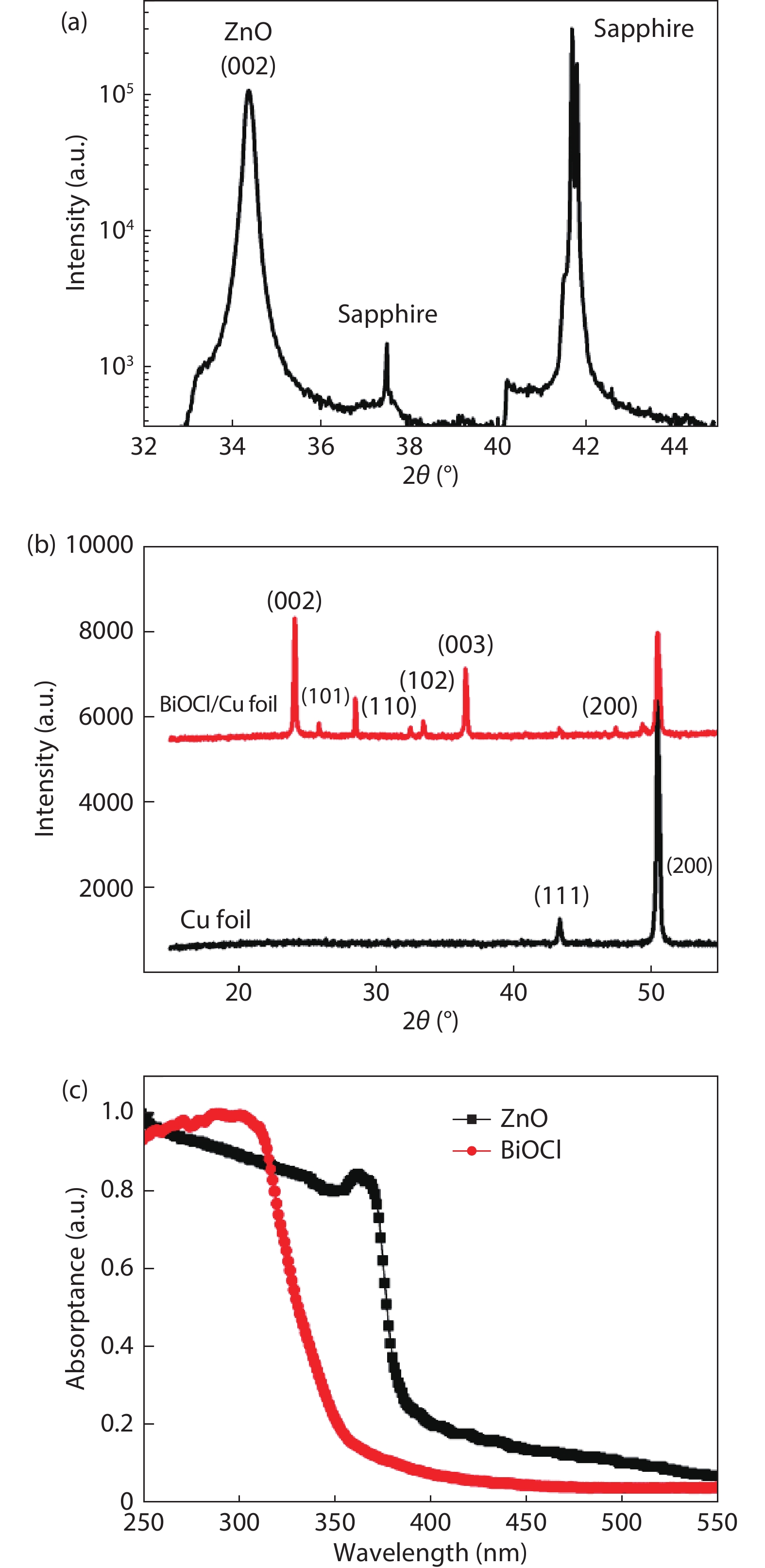
    Fig. 1. (Color online) (a) XRD pattern of ZnO thin film. (b) XRD patterns of BiOCl on Cu foil substrate and Cu foil. (c) Optical absorption spectra of BiOCl nanoflakes and ZnO thin film.
    SEM images of BiOCl on Cu foil at different levels of magnification.
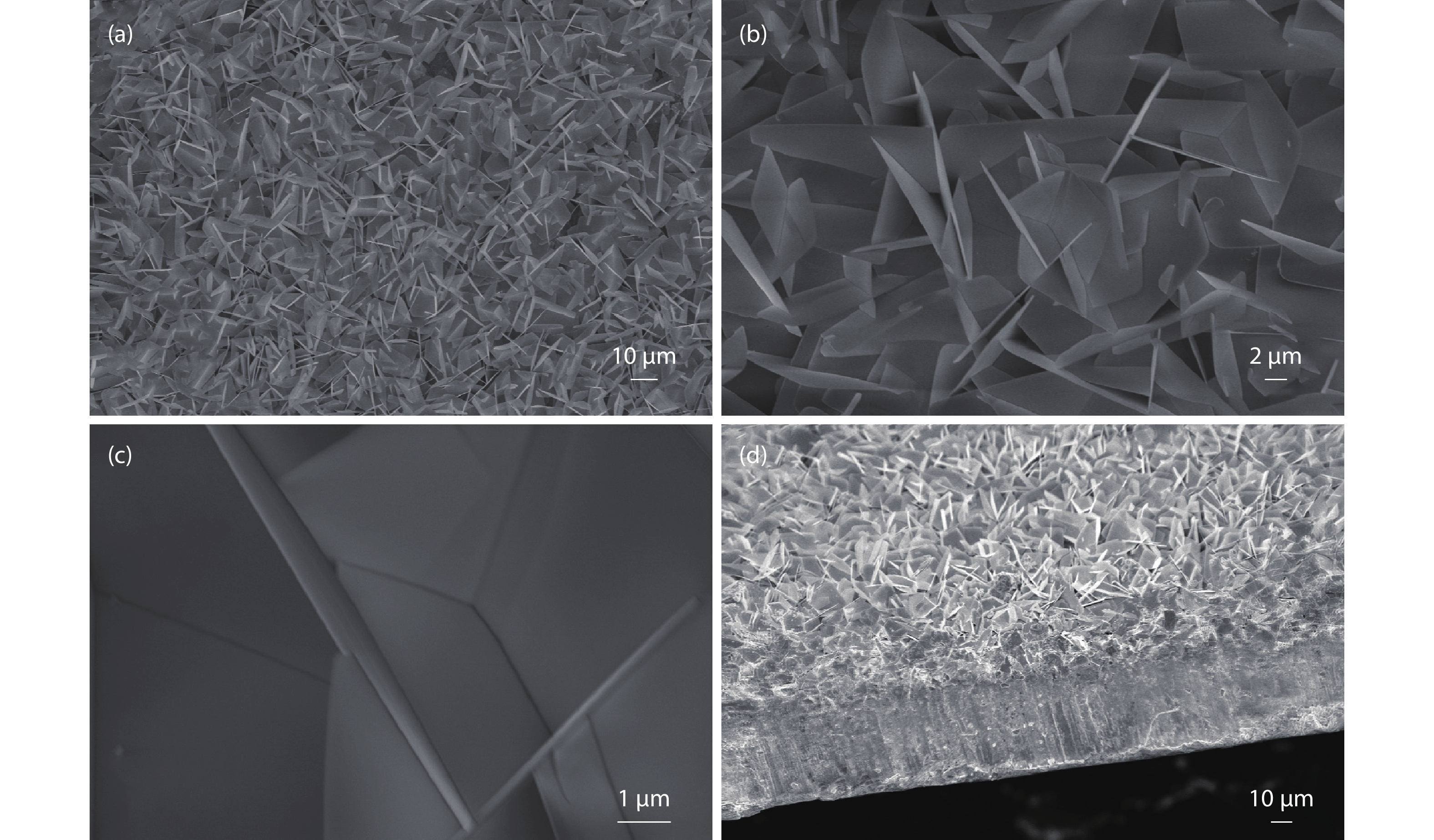
    Fig. 2. SEM images of BiOCl on Cu foil at different levels of magnification.
    (Color online) (a) Top view AFM image of ZnO thin film at a scale of 5 × 5 μm2. (b) Section profile of ZnO thin film. (c) 3D AFM image of ZnO thin film.
    Fig. 3. (Color online) (a) Top view AFM image of ZnO thin film at a scale of 5 × 5 μm2. (b) Section profile of ZnO thin film. (c) 3D AFM image of ZnO thin film.
    (a) TEM image, (b) HRTEM image, and (c) SAED pattern of the BiOCl nanoflakes samples.
    Fig. 4. (a) TEM image, (b) HRTEM image, and (c) SAED pattern of the BiOCl nanoflakes samples.
    (Color online) (a) Schematic diagram of the p-BiOCl/n-ZnO photodetector with back-side light irradiation. (b) I–V curve of In–ZnO–In device in dark. (c) I–V curve of p-BiOCl/n-ZnO photodetector in dark, inset is the I–V curves of the device in dark and under 350 nm light illumination at logarithmic scale. (d) I–V curve of Cu–BiOCl–Cu device in dark. (e) Logarithmic scale I–V curves of In–ZnO–In device in dark and under 350 nm light illumination. (f) Logarithmic scale I–V curves of Cu-BiOCl-Cu device in dark and under 350 nm light illumination.
    Fig. 5. (Color online) (a) Schematic diagram of the p-BiOCl/n-ZnO photodetector with back-side light irradiation. (b) I–V curve of In–ZnO–In device in dark. (c) I–V curve of p-BiOCl/n-ZnO photodetector in dark, inset is the I–V curves of the device in dark and under 350 nm light illumination at logarithmic scale. (d) I–V curve of Cu–BiOCl–Cu device in dark. (e) Logarithmic scale I–V curves of In–ZnO–In device in dark and under 350 nm light illumination. (f) Logarithmic scale I–V curves of Cu-BiOCl-Cu device in dark and under 350 nm light illumination.
    (Color online) The photoresponse spectra of the p-BiOCl/n-ZnO photodetector at different (a) negative biases and (b) positive biases. (c) Schematic energy band diagram of the device.
    Fig. 6. (Color online) The photoresponse spectra of the p-BiOCl/n-ZnO photodetector at different (a) negative biases and (b) positive biases. (c) Schematic energy band diagram of the device.
    (Color online) (a) Time response (“on” and “off” states) characteristic of the p-BiOCl/n-ZnO photodetector under 350 nm (0.304 mW/cm2), 400 nm (0.386 mW/cm2), and 450 nm (0.426 mW/cm2) light illumination at –3 V. (b) Normalized time response of the p-BiOCl/n-ZnO photodetector under 350 nm (0.304 mW/cm2) illumination at –3 V. (c) Single period time response of the In–ZnO–In photodetector under 350 nm (0.304 mW/cm2) illumination at –3 V. (d) Single period time response of the Cu–BiOCl–Cu photodetector under 350 nm (0.304 mW/cm2) illumination at 3 V.
    Fig. 7. (Color online) (a) Time response (“on” and “off” states) characteristic of the p-BiOCl/n-ZnO photodetector under 350 nm (0.304 mW/cm2), 400 nm (0.386 mW/cm2), and 450 nm (0.426 mW/cm2) light illumination at –3 V. (b) Normalized time response of the p-BiOCl/n-ZnO photodetector under 350 nm (0.304 mW/cm2) illumination at –3 V. (c) Single period time response of the In–ZnO–In photodetector under 350 nm (0.304 mW/cm2) illumination at –3 V. (d) Single period time response of the Cu–BiOCl–Cu photodetector under 350 nm (0.304 mW/cm2) illumination at 3 V.
    Longxing Su, Weixin Ouyang, Xiaosheng Fang. Facile fabrication of heterostructure with p-BiOCl nanoflakes and n-ZnO thin film for UV photodetectors[J]. Journal of Semiconductors, 2021, 42(5): 052301
    Download Citation