
Longxing Su, Weixin Ouyang, Xiaosheng Fang. Facile fabrication of heterostructure with p-BiOCl nanoflakes and n-ZnO thin film for UV photodetectors[J]. Journal of Semiconductors, 2021, 42(5): 052301
- Journal of Semiconductors
- Vol. 42, Issue 5, 052301 (2021)
Abstract
1. Introduction
UV photodetectors have received considerable attention in recent years thanks to their broad range of applications, including environmental monitoring, space communication, biological sensing and missile plume sensing[
UV photodetectors fabricated with wide bandgap materials have been widely investigated and reported, such as Ga2O3[
Bismuth oxyhalides are ternary alloy semiconductors with a chemical expression of [BilOmXn], where X = I, Cl, or Br[
Herein, we report a photodetector by constructing a heterojunction with high-quality n-type ZnO thin film and p-type BiOCl nanoflakes. A noticeable rectification characteristic is observed through the I–V curves in dark, indicating the successful formation of a heterojunction. The photodetector demonstrates excellent UV light selectivity and its on/off ratio (I350 nm/Idark) reaches as high as 800. However, the on/off ratio of In–ZnO–In photodetector and Cu–BiOCl–Cu photodetector are ~20 and less than 2, respectively. The improvement is ascribed to the more efficient separation of photo-excited carriers forced by the built-in electric field. The device also demonstrates shorter response time (rise time of 12.6 s, decay time of 0.95 s) than those devices fabricated on pure n-ZnO and p-BiOCl. This low-cost fabrication strategy of constructing ZnO-film-based p–n heterostructure envisages a profound impact on the next generation ZnO-based photodetectors.
2. Experimental
2.1. Preparation of ZnO thin film on sapphire substrate
We utilized the RF (radio frequency) plasma assisted molecular beam epitaxy (MBE) technique to synthesize the ZnO film layer. Prior to the growth of ZnO, the substrate and Zn source were preheated to 650 and 340 °C, respectively. In the growth process, the flux rate of oxygen was steadied at 120 sccm, the RF power was kept at 400 W.
2.2. Preparation of BiOCl nanoflakes on Cu foil
0.1577 g of BiCl3 and 3.3 mL of concentrated HCl were added into 95 mL mixture solvent of ethylene glycol and H2O (volume ratio: 10 : 85). After the mixed solution was stirred and heated to 70 °C, 1 mL of 30% H2O2 solution was added into this solution. Then, a piece of clean copper foil was immersed into this solution for 1 h. After being washed by absolute alcohol three times, and then dried at 60 °C for 1 h, the obtained sample was kept in a storage for further use. We bought all these chemical reagents from the Sinopharm Company and they were used as received.
2.3. Characterization
To investigate their crystal structures and quality, we acquired the X-ray diffraction (XRD) patterns of the samples by a Bruker D8-A25 diffractometer using Cu Kα radiation (λ = 1.5405 Å). The absorption spectra were recorded on a Hitachi U3900H UV–Vis–NIR scanning spectrophotometer. The morphologies and microstructures of the samples were examined by a field-emission scanning electron microscopy (FESEM) from Zeiss Sigma company and a high-resolution transmission electron microscopy (HRTEM) from TECNAI company, respectively. We employed an atomic force microscope from Bruker company to characterize the surface properties of ZnO film layer.
2.4. Device fabrication and photoelectric measurement
The p-BiOCl/n-ZnO heterostructured photodetector was prepared by mechanical bonding of two different materials and then annealed at 100 °C for 0.5 h. Cu foil and metal Indium pad were used as the electrodes to contact with the p-BiOCl and n-ZnO, respectively. The photoelectric performance of the as-constructed device was studied through a Xe lamp equipped with monochromator as the light source, and a Keithley 4200 semiconductor characterization system as the analyzer. A NOVA II power meter from OPHIR photonics was utilized to measure the optical power density-wavelength curve of the light source. We conducted all of the measurements in air ambient.
3. Results and discussion
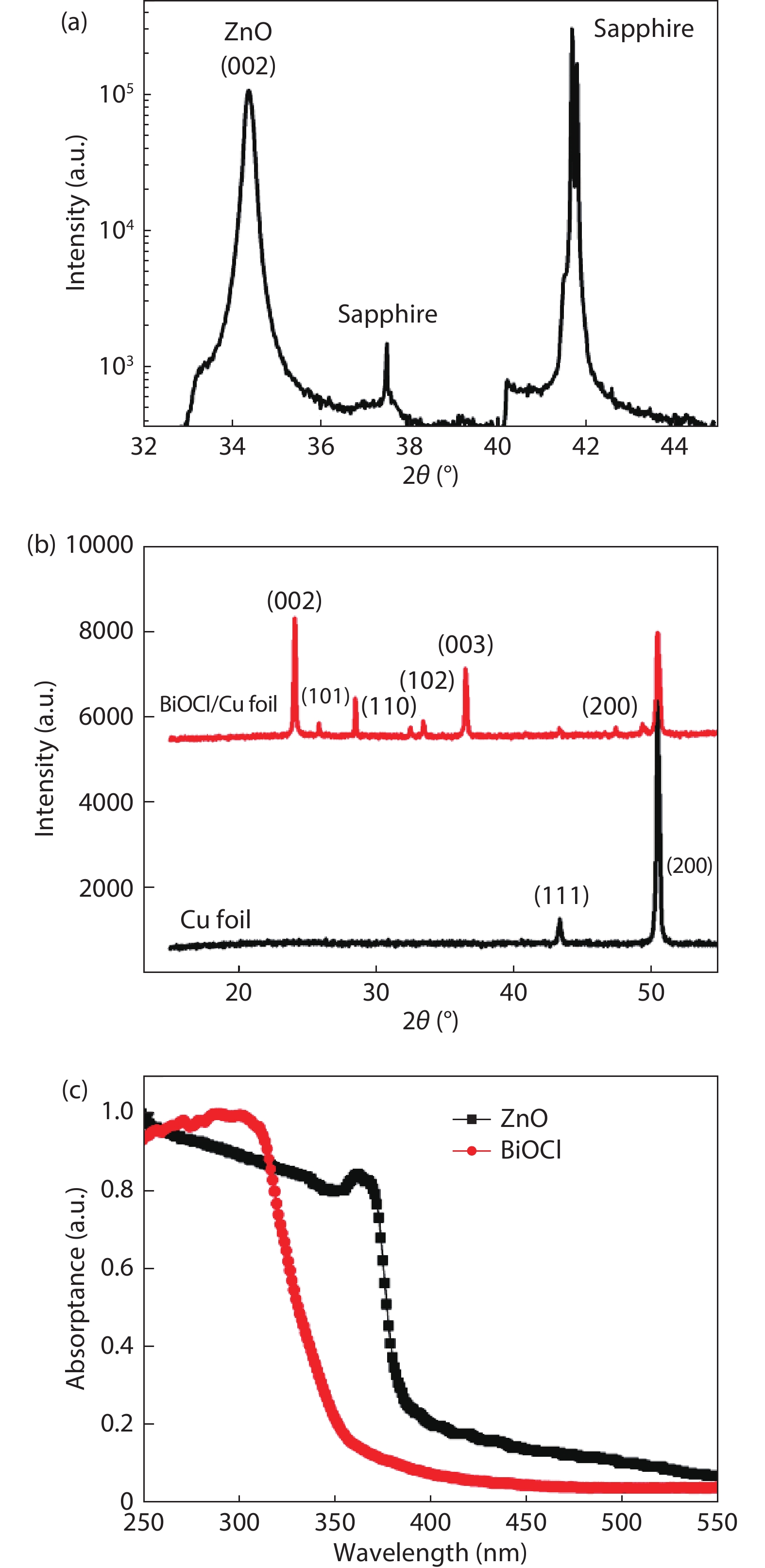
Fig. 1(a) illustrates the XRD results of ZnO film layer on sapphire substrate. Apart from the characteristic diffraction peaks from the sapphire substrate, only one diffraction peak centered at around 34.4° is found. This peak originates from the (002) diffraction signal of wurtzite ZnO and reveals its c direction growth preference. The full width at half maximum (FWHM) of this peak is only 0.22°. Fig. 1(b) displays the XRD results of the BiOCl nanoflakes on Cu foil and Cu foil, it is seen that all the main diffraction peaks from the obtained BiOCl sample on Cu foil are indexed to the (002, 110, 102, 003, and 200) facets of tetragonal BiOCl (JCPDS No. 6-249). Two weak diffraction peaks that resulted from the byproducts and residual of reactants are also detected. The sharp and intense diffraction peaks suggest that the as-synthesized BiOCl sample is well-crystallized. In addition, the intensity of the diffraction peaks from (002) and (003) facets are stronger than the peak intensities of the other facets, which may indicate the favored growth orientations of the BiOCl. To estimate the bandgaps of these materials, optical absorption spectra of BiOCl sample and ZnO thin film are tested. Fig. 1(c) presents the normalized absorption spectra of BiOCl and ZnO, the absorption edges of both materials are located at the UVA range. The cut-off absorption edge located at ~375 nm can be ascribed to the ZnO film layer and the cut-off absorption edge at ~345 nm is ascribed to the BiOCl nanoflakes. Therefore, the bandgaps of the as prepared ZnO and BiOCl materials are confirmed as ~3.3 and ~3.5 eV.
![]()
Figure 1.(Color online) (a) XRD pattern of ZnO thin film. (b) XRD patterns of BiOCl on Cu foil substrate and Cu foil. (c) Optical absorption spectra of BiOCl nanoflakes and ZnO thin film.
Fig. 2 reveals the morphology and crystal structures of BiOCl nanoflakes. From the top view scanning electron microscopy (SEM) images in Figs. 2(a) and 2(b), it can be seen that the BiOCl nanoflakes are homogeneously and densely grown on the entire surface of Cu foil, neighboring nanoflakes are connected with each other to form arrays. From the magnified SEM image in Fig. 2(c), the individual nanoflakes present even and smooth dominant surfaces and their thicknesses are estimated to be several tens of nanometers. The side view SEM pattern of BiOCl nanoflakes on Cu foil is illustrated in Fig. 2(d), and a distinct and coarse boundary between the BiOCl nanoflakes and the Cu foil is presented. The average height of the BiOCl nanoflake arrays is estimated to be ~ 20 μm. Fig. 3 presents the surface fluctuation of the ZnO film layer. The root-mean-square roughness over 5 × 5 μm2 area is only ~0.85 nm and the section profile (white line in Fig. 3(a)) shown in Fig. 3(b) indicates that the maximum surface fluctuation is < 1.2 nm. 3D atomic force microscopy (AFM) image of the ZnO film layer ( Fig. 3(c)) presents the homogenous distribution of hexagonal pyramids. The AFM measurement indicates a smooth surface morphology of the ZnO film layer prepared by MBE. The dense distribution and conformal coverage of the BiOCl nanoflake arrays on the Cu foil and the smooth surface of ZnO thin film can ensure their intimate contact after the post annealing process, which is beneficial for the carrier transport in the heterostructure photodetector.
![]()
Figure 2.SEM images of BiOCl on Cu foil at different levels of magnification.
![]()
Figure 3.(Color online) (a) Top view AFM image of ZnO thin film at a scale of 5 × 5
Fig. 4(a) shows a transmission electron microscopy (TEM) image of the BiOCl nanoflakes on Cu foil substrate. Here, the BiOCl nanoflakes sample was scraped down and then transferred to the Cu mesh for the TEM measurement. The nanoflake’s surface presents flat and uniform properties. The clear lattice fringes in high-resolution TEM (HRTEM) image (Fig. 4(b)) illustrates the high crystal quality of the nanoflake prepared by this chemical bath method. The interplanar lattice spacing is 0.275 nm, corresponding to the (110) planes of tetragonal BiOCl. In addition, the selected-area electron diffraction (SAED) measurement (Fig. 4(c)) indicates the single-crystalline property of the BiOCl nanoflakes. A 45° angle is labeled between two sets of SAED spots, which perfectly agrees well with the angle between (200) and (110) planes. These diffraction spots can be confirmed as the [001] zone axis of tetragonal BiOCl. In addition, considering the crystal symmetries of BiOCl and the previous results, the dominant surface of the BiOCl nanoflakes is identified as (001) facet.
![]()
Figure 4.(a) TEM image, (b) HRTEM image, and (c) SAED pattern of the BiOCl nanoflakes samples.
The photoelectric characteristics were systematically studied by employing a two-probe technique in ambient. The device configuration is shown in Fig. 5(a). Metal indium pad is utilized to prepare an Ohmic contact with ZnO, the Cu foil naturally achieves an Ohmic contact with the BiOCl nanoflakes. Both metal indium pad and Cu foil are bonded with Cu wires and then connected with two probes. In this configuration, the incident light is irradiated from the back side where the sapphire (Eg ~ 7.6 eV) substrate can act as a transparent window to the incident light. As revealed in Fig. 5(c), the I–V curve recorded in the dark illustrates that this as-fabricated photodetector features a rectifying characteristic. The turn-on voltage is ~3.2 V and the ratio is ~66 at ±4 V biases. For comparison, an In–ZnO–In device consisting of ZnO film and two pieces of indium pads as electrodes, and a Cu–BiOCl–Cu device consisting of BiOCl nanoflakes and two pieces of Cu foils as electrodes were fabricated. Figs. 5(b) and 5(d) present the I–V results of In–ZnO–In device and Cu–BiOCl–Cu device in dark, respectively. It is clearly shown that both currents have a linear correlation with the voltages. Hence, the contacts between indium pads and ZnO film, as well as the contacts between BiOCl nanoflakes and Cu foil are Ohmic contacts. Therefore, the rectifying characteristic of the photodetector originates from the p-BiOCl/n-ZnO heterojunction. The effects of Schottky junction between semiconductors and metal electrodes on the rectifying characteristic can thus be excluded. The inset of Fig. 5(c) presents the I–V curves under dark and UV light irradiation (350 nm). Under –5 V bias, the photocurrent value under 350 nm light irradiation is ~800 times of that in dark, which indicates that the p-BiOCl/n-ZnO device shows a strong response to UV light. However, for In–ZnO–In photoconductive device, the on/off ratio at 350 nm is only ~20. In addition, the Cu–BiOCl–Cu photoconductive device has a very weak response to UV light. Therefore, it is concluded that the strong response of p-BiOCl/n-ZnO photoconductor to UV light is due to the characteristics of the heterostructure.
![]()
Figure 5.(Color online) (a) Schematic diagram of the p-BiOCl/n-ZnO photodetector with back-side light irradiation. (b)
Responsivity (Rλ) is a key parameter to estimate the sensitivity of the photodetector. It can be calculated by the equation of Rλ = (Iλ– Id)/PλS, where Iλ, Id and S are the photocurrent and dark current of the device’s effective area under irradiation, respectively. Fig. 6 presents the spectral responsivities of p-BiOCl/n-ZnO heterostructure photodetector under different biases. A clear cut-off wavelength at around 380 nm is found, which corresponds well with the absorption edge of ZnO. In addition, the responsivity increases as the external bias increases and the maximum responsivity under –5 V is ~0.15 A/W. This indicates that the active layer of the device under negative biases is mainly located on the ZnO side. It is worth noting that the spectral response curves (Fig. 6(b)) at positive biases are different from those under negative biases (Fig. 6(a)). Additional weak response signals found at around 320 nm are ascribed to the intrinsic photoresponse of BiOCl nanoflakes. The different responsivities under negative and positive biases can be ascribed to the variation of the depletion layer depth. As the positive bias increases, the deletion layer depth decrease because of the inner potential offset. Therefore, the equivalent circuit of p-BiOCl/n-ZnO photodetector can be regarded as a series of BiOCl photosensitive resistors, p–n junctions, and ZnO photosensitive resistors. Because the BiOCl nanoflakes are well-aligned on the surface of the Cu foil, the photogenerated carriers in BiOCl photosensitive layer can be easily collected and effectively contributed to the photocurrent. Thus, intrinsic response of BiOCl nanoflakes is shown under positive biases. Typically, the detectivity D* demonstrates the noise equivalent power (NEP) in a device and can be defined as: D* = Rλ(2eId/S)–1/2, where e is the elementary charge constant. Fig. S1 depicts the wavelength dependent detectivity of p-BiOCl/n-ZnO UV photodetector at different bias voltages. Obviously, the device shows high detectivity of > 10 11 Jones at different bias voltages, which demonstrates the device’s excellent capability to detect signals from noise environment. Fig. 6(c) presents the energy band diagram of the p-BiOCl/n-ZnO heterostructure, where a type-II band structure is formed. Thus, the as-generated built-in electric field can effectively separate the photo-induced electron-hole pairs, contributing to the superior performance of the photodetector, and even making the photodetector operate under 0 V bias. Figs. S2 and S3 present the photoresponse of this heterostructure device under 0 V bias, from which the photodetector is deemed as a self-powered device. However, the photodetector shows relatively poor performance without external bias voltage, mainly because of the mechanical contacted interface between p-BiOCl and n-ZnO. Further strategies such as directly grown p-BiOCl nanoflakes on n-ZnO film layer can be considered to improve the hetero-interface, and thus the photodetector can work as a high performance photovoltaic type device.
![]()
Figure 6.(Color online) The photoresponse spectra of the p-BiOCl/n-ZnO photodetector at different (a) negative biases and (b) positive biases. (c) Schematic energy band diagram of the device.
Fig. 7(a) displays the on/off switching current states of p-BiOCl/n-ZnO photodetector under 350 nm (0.304 m/cm2), 400 nm (0.386 mW/cm2), and 450 nm (0.426 mW/cm2) light illuminations at –3 V, respectively. Although the optical power density increases, the photocurrent decreases as the irradiation wavelength increases. The dark current nearly coincidences with the photocurrent under 450 nm light illumination, indicating the excellent UV light selectivity of this device. According to the I–T curve shown in Fig. 7(b), the rise time (from 10% to 90% of the maximum current) and decay time (from 90% to 10% of the maximum current) are calculated as 12.6 and 0.95 s, respectively. Typically, owing to the surface states caused by the defects like oxygen vacancies, ZnO based photoconductive-type photodetector exhibits extremely slow response time (typically several minutes). As presented in Fig. 7(c), the response time of the In–ZnO–In photoconductive device are calculated to be 18 s (rise time) and 70.7 s (decay time). Thus, the decay speed of the p-BiOCl/n-ZnO photodetector is almost 74 times faster than that of the In–ZnO–In photoconductive device. Here, the tiny improvement of rise time resultes from the relatively incomplete mechanical contact between p-BiOCl and n-ZnO. Due to a low on/off ratio of 1.15 (Fig. 7(d)), the response time of Cu–BiOCl–Cu photoconductive device could not be calculated. In general, the response speed is significantly improved through the formation of a p-BiOCl/n-ZnO heterojunction.
![]()
Figure 7.(Color online) (a) Time response (“on” and “off” states) characteristic of the p-BiOCl/n-ZnO photodetector under 350 nm (0.304 mW/cm2), 400 nm (0.386 mW/cm2), and 450 nm (0.426 mW/cm2) light illumination at –3 V. (b) Normalized time response of the p-BiOCl/n-ZnO photodetector under 350 nm (0.304 mW/cm2) illumination at –3 V. (c) Single period time response of the In–ZnO–In photodetector under 350 nm (0.304 mW/cm2) illumination at –3 V. (d) Single period time response of the Cu–BiOCl–Cu photodetector under 350 nm (0.304 mW/cm2) illumination at 3 V.
4. Conclusion
In conclusion, a novel UV photodetector constructed with the n-type ZnO thin film and p-type BiOCl nanoflakes is successfully realized through a facile fabrication process. The wurtzite n-ZnO thin film with preferred c-axis growth direction and low concentration of defects is prepared by MBE on a c-sapphire substrate, while the p-BiOCl nanoflakes are grown on a Cu foil by a simple chemical bath technique. Subsequently, this heterostructure photodetector is assembled through mechanical bonding and post-annealing of two materials. The p-BiOCl/n-ZnO device exhibits a high UV–visible rejection ratio of 102 and a faster response time than those of pure ZnO and BiOCl based photodetectors. In addition, the on/off ratio of the photodetector achieves as large as 800 under –5 V, which is also much higher than those of pure ZnO and BiOCl based photodetectors. This work provides an effective and facile way for preparing high performance heterostructure photodetectors, suggesting its potential applications in future optoelectronic devices.
Acknowledgements
Dr. Longxing Su and Dr. Weixin Ouyang contributed equally to this work. The authors would like to thank Dr. Xiaojie Xu and Miss Yihan Chen for their kind help.
This work is supported by the National Natural Science Foundation of China (Grant No. 61705043, 51872050 and 11811530065), the National Key Research and Development Program of China (Grant No. 2017YFA0204600), the Natural Science Foundation of Jiangsu Province (No. BK20160568); National Postdoctoral Science Foundation of China (Grant No. 2017M611411, 2018M640338, 2018T110344 and 2019T120299) and the Ministry of Education Joint Fund for Equipment Pre-Research (6141A02033241).
Appendix A. Supplementary materials
Supplementary materials to this article can be found online at https://doi.org/1674-4926/42/5/052301.
References
[1] H Y Chen, K W Liu, L F Hu et al. New concept ultraviolet photodetectors. Mater Today, 18, 493(2015).
[2] Z Lou, X L Yang, H R Chen et al. Flexible ultraviolet photodetectors based on ZnO-SnO2 heterojunction nanowire arrays. J Semicond, 39, 024002(2018).
[3] L X Su, W Yang, J Cai et al. Self-powered ultraviolet photodetectors driven by built-in electric field. Small, 13, 1701687(2017).
[4] X J Xu, J X Chen, S Cai et al. A real-time wearable UV-radiation monitor based on a high-performance p-CuZnS/n-TiO2 photodetector. Adv Mater, 30, 1803165(2018).
[5] L W Sang, M Y Liao, M Sumiya. A comprehensive review of semiconductor ultraviolet photodetectors: from thin film to one-dimensional nanostructures. Sensors, 13, 10482(2013).
[6] SY Li, Y Zhang, W Yang et al. 2D perovskite Sr2Nb3O10 for high-performance UV photodetectors. Adv Mater, 32, 1905443(2020).
[7] G Konstantatos, A Levina et al. Engineering the temporal response of photoconductive photodetectors via selective introduction of surface trap states. Nano Lett, 8, 1446(2008).
[8] Y Z Jin, J P Wang, B Q Sun et al. Solution-processed ultraviolet photodetectors based on colloidal ZnO nanoparticles. Nano Lett, 8, 1649(2008).
[9] B Zhao, F Wang, H Y Chen et al. An ultrahigh responsivity (9.7 mA W–1) self-powered solar-blind photodetector based on individual ZnO-Ga2O3 heterostructures. Adv Funct Mater, 27, 1700264(2017).
[10] W Y Kong, G A Wu, K Y Wang et al. Graphene-
[11] X M Chen, K W Liu, Z Z Zhang et al. A self-powered solar-blind photodetector with fast response based on Au/
[12] A S Pratiyush, S Krishnamoorthy, S V Solanke et al. High responsivity in molecular beam epitaxy grown
[13] F G Posada, R Songmuang, M D Hertog et al. Room-temperature photodetection dynamics of single GaN nanowires. Nano Lett, 12, 172(2012).
[14] B Butuna, T Tut, E Ulker et al. High-performance visible-blind GaN-based p–i–n photodetectors. Appl Phys Lett, 92, 033507(2008).
[15] G Y Xu, A Salvador, W Kim et al. High speed, low noise ultraviolet photodetectors based on GaN p–i–n and AlGaN(p)-GaN(i)-GaN(n) structures. Appl Phys Lett, 71, 2154(1997).
[16] L X Zheng, P P Yu, K Hu et al. Scalable-production, self-powered TiO2 nanowell-organic hybrid UV photodetectors with tunable performances. ACS Appl Mater Inter, 8, 33924(2016).
[17] X D Li, C T Gao, H G Duan et al. Nanocrystalline TiO2 film based photoelectrochemical cell as self-powered UV-photodetector. Nano Energy, 1, 640(2012).
[18] M Patel, H S Kim, J Kim. All transparent metal oxide ultraviolet photodetector. Adv Electron Mater, 1, 1500232(2015).
[19] Z Chen, B R Li, X M Mo et al. Self-powered narrowband p-NiO/n-ZnO nanowire ultraviolet photodetector with interface modification of Al2O3. Appl Phys Lett, 110, 123504(2017).
[20] J Cai, X J Xu, L X Su et al. Self-powered n-SnO2/p-CuZnS core-shell microwire UV photodetector with optimized performance. Adv Opt Mater, 6, 1800213(2018).
[21] X J Xu, S Shukla, Y Liu et al. Solution-processed transparent self-powered p-CuS-ZnS/n-ZnO UV Photodiode. Phys Status Solidi RRL, 12, 1700381(2018).
[22] L X Su, Q L Zhang, T Z Wu et al. High-performance zero-bias ultraviolet photodetector based on p-GaN/n-ZnO heterojunction. Appl Phys Lett, 105, 072106(2014).
[23] L X Su, Y Zhu, D Y Yong et al. Wide range bandgap modulation based on ZnO-based alloys and fabrication of solar blind UV detectors with high rejection ratio. ACS Appl Mater Inter, 6, 14152(2014).
[24] T H Moon, M C Jeong, W Lee et al. The fabrication and characterization of ZnO UV detector. Appl Surf Sci, 240, 280(2005).
[25] Z N Wang, R M Yu, X F Wang et al. Ultrafast response p-Si/n-ZnO heterojunction ultraviolet detector based on pyro-phototronic effect. Adv Mater, 28, 6880(2016).
[26] S Liang, H Sheng, Y Liu et al. ZnO Schottky ultraviolet photodetectors. J Cryst Growth, 225, 110(2001).
[27] S J Pearton, D P Norton, K Ip et al. Recent progress in processing and properties of ZnO. Prog Mater Sci, 50, 293(2005).
[28] Ü Özgüra, Y I Alivov, C Liu et al. A comprehensive review of ZnO and related devices. J Appl Phys, 98, 041301(2005).
[29] H Shen, C Shan, B Li et al. Reliable self-powered highly spectrum-selective ZnO ultraviolet photodetectors. Appl Phys Lett, 103, 232112(2013).
[30] H D Cho, A S Zakirov, S U Yuldashev et al. Photovoltaic device on a single ZnO nanowire p –n homojunction. Nanotechnology, 23, 115401(2012).
[31] K Hu, F Teng, L X Zheng et al. Binary response Se/ZnO p–n heterojunction UV photodetectorrnwith high on/off ratio and fast speed. Laser Photonics Rev, 11, 1600257(2017).
[32] H Y Chen, P P Yu, Z M Zhang et al. Ultrasensitive self-powered solar-blind deep-ultraviolet photodetector based on all-solid-state polyaniline/MgZnO bilayer. Small, 12, 5809(2016).
[33] J Li, H Li, G Zhan et al. Solar water splitting and nitrogen fixation with layered bismuth oxyhalides. Acc Chem Res, 50, 112(2017).
[34] X Y Huang, B Li, H Guo. Synthesis, photoluminescence, cathodoluminescence and thermal properties of novel Tb3+-doped BiOCl green-emitting phosphors. J Alloy Compd, 695, 2773(2017).
[35] Y W Zhang, X H Xu, Y Xing et al. Growth and electronic transport property of layered BiOCl microplates. Adv Mater Interfaces, 2, 1500194(2015).
[36] S Dutta, T Das, S Datta. Impact of bi-axial strain on structural, electronic and optical properties of photo-catalytic bulk bismuth oxy-halides. Phys Chem Chem Phys, 20, 103(2018).
[37] A Dash, S Sarkar, V N K B Adusumalli et al. Microwave synthesis, photoluminescence, and photocatalytic activity of PVA-functionalized Eu3+ -doped BiOX (X = Cl, Br, I) nanoflakes. Langmuir, 30, 1401(2014).
[38] Y J Li, Q Wang, B C Liu et al. The {001} facets-dependent superior photocatalytic activities of BiOCl nanosheets under visible light irradiation. Appl Surf Sci, 349, 957(2015).
[39] G K Tripathi, R Kurchania. Photocatalytic behavior of BiOX (X = Cl/Br, Cl/I and Br/I) composites/heterogeneous nanostructures with organic dye. Opt Quant Electron, 49, 203(2017).
[40] H F Cheng, B B Huang, Y Dai. Engineering BiOX (X = Cl, Br, I) nanostructures for highly efficient photocatalytic applications. Nanoscale, 6, 2009(2014).
[41] Y X Yu, W X Ouyang, W D Zhang. Photoelectrochemical property of the BiOBr-BiOI/ZnO heterostructures with tunable bandgap. J Solid State Electrochem, 18, 1743(2014).
[42] F Teng, W X Ouyang, Y M Li et al. Novel structure for high performance UV photodetector based on BiOCl/ZnO hybrid film. Small, 13, 1700156(2017).

Set citation alerts for the article
Please enter your email address
© Copyright 2018-2021 | Chinese Laser Press. All Rights Reserved 沪ICP备15018463号-20