Xiaoze Liu, Xinyuan Zhang, Shunping Zhang, Zhiqiang Guan, Hongxing Xu. Light-Matter Coupling of Two-Dimensional Semiconductors in Micro-Nano Optical Cavities[J]. Acta Optica Sinica, 2021, 41(8): 0823003
Search by keywords or author
- Acta Optica Sinica
- Vol. 41, Issue 8, 0823003 (2021)
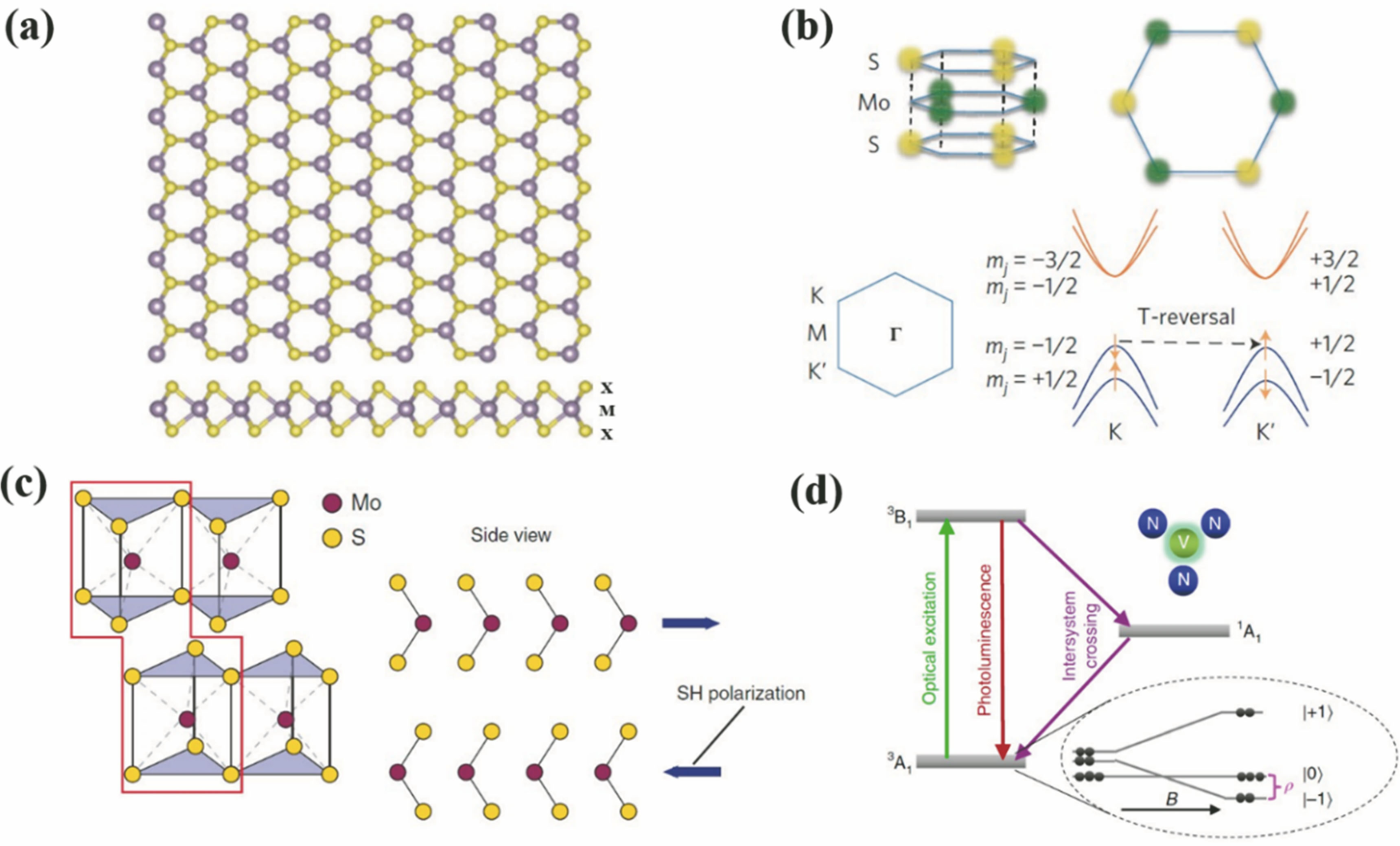
![Schematics for some fundamental properties of 2D semiconductors. (a) Schematic of atomic structure of TMD MX2[13]; (b) upper: triangular prismatic structure and honeycomb lattice structure of monolayer MoS2; lower: hexagonal structure of valley band of degenerate states (K and K') and selection rule of valley band transition[36]; (c) 2H phase of monolayer TMD hexagonal lattice and SHG under symmetry breaking of spatial inversion[37]; (d) schematic of single photon properties of defect states in 2D materials[38]](/richHtml/gxxb/2021/41/8/0823003/img_1.jpg)
Fig. 1. Schematics for some fundamental properties of 2D semiconductors. (a) Schematic of atomic structure of TMD M
![Optical control for 2D semiconductors. (a) Relationship between PL intensity of charged exciton and exciton X0 and gate voltage Vg[72]. Solid line is model curve predetermined by theory; (b) electrical control of SHG resonance intensity with gated voltage[49]; (c) schematic of Zeeman effect under magnetic field for degenerate valley electronic energy band[80]; (d) schematic of Stark effect under ultrafast optical field for degenerate valley electronic energy band[81]](/richHtml/gxxb/2021/41/8/0823003/img_2.jpg)
Fig. 2. Optical control for 2D semiconductors. (a) Relationship between PL intensity of charged exciton and exciton X0 and gate voltage
Fig. 3. Fundamental features of 2D heterostructures. (a) Configuration of energy band of type-II heterostructures. Magnified image depicts spatially indirect interlayer exciton[98]; (b) schematic of twist angle-dependent Moiré lattice in 2D heterostructures
Fig. 4. Schematics of various micro/nano-cavities. (a) Schematic of FP optical cavity with two DBRs; (b) schematic of WGM cavity formed by total reflection along ring perimeter; (c) schematic of PCC with photonic crystal defect nanocavity[6]; (d) schematic of PCC of BIC mode[122]; (e) schematic of plasmonic nanocavity[126]
Fig. 5. Schematics of CQED principles. (a) Schematic of coupling process between excitons and cavity photons; (b) schematic of fluorescence enhancement of Purcell effect in weak coupling regime; (c) schematic of anti-crossed exciton polaritons in strong coupling regime. P+ (P-) represents upper (lower) polaritons
Fig. 6. Weak coupling regime of 2D semiconductors and dielectric micro/nano-cavities. (a) Purcell effect of weak coupling between monolayer MoS2 and PCC nanocavity. Purcell effect has polarization dependence on optical cavity[141]; (b) schematic of ultra-low threshold laser of monolayer WSe2 in PCC nanocavity[143]; (c) schematic of monolayer WS2 microdisk laser[144]; (d) schematic of CW near-infrared laser of monolayer MoTe2 nanobeam cavity at room temperature[145]; (e) structural diagram of monolayer WS2 VCSEL[146]
Fig. 7. Weak coupling regime of 2D semiconductors and plasmonic nanocavities. (a) Purcell effect of weak coupling between plasmonic nanocavity and 2D semiconductor for enhancing Raman and fluorescence intensities[149]; (b) control of valley degree of freedom through coupling between plasmonic nanocavity and 2D semiconductor[140]; (c) weak coupling of quantum emitters with defect in monolayer WSe2 and plasmonic nanocavities[69]
Fig. 8. Strong coupling regime of 2D semiconductors and plane FP microcavities. (a) Structural diagram for first demonstration of strong coupling between monolayer MoS2 and FP microcavity at room temperature[155]; (b) structural diagram for strong coupling between monolayer MoSe2 and open FP microcavity[156]; (c) schematic of 2D polarized exciton polaritons with valley degree of freedom in strong coupling regime; (d) schematics of nonlinear optical principles of 2D polarized exciton polaritons in strong coupling regime[161]; (e) optical valley Hall effects based on nonlinear optical response of 2D exciton polaritons in strong coupling regime[162]; (f) structural schematic of open FP microcavity for control of 2D exciton polariton and polaron via carrier concentration in strong coupling regime[163]; (g) structural schematic of sample for realization of electrically pumped 2D exciton polaritons in strong coupling regime[164]
Fig. 9. Strong coupling regime of 2D semiconductors and micro/nano-cavities with different structures. (a) Sample schematic for realizing strong coupling between monolayer WSe2 and plasmonic nanocavity[173]; (b) sample microscopic image with strong coupling between monolayer MoSe2 and plasmonic array[178];(c) sample schematic for the strong coupling between monolayer TMD and one-dimensional PCC[135]; (d) sample schematic with strong coupling between monolayer WS2 and BSW mode in DBR substrate[183]
Fig. 10. Laser generated by coupling between PCC nanocavity and interlayer excitons of 2D semiconductor heterostructures. (a) Sample schematic for lasing actions based on coupling between 2D semiconductor WSe2/MoSe2 heterostructure and one-dimensional PCC nanocavity[184]; (b) schematic for lasing principles based on coupling between 2D semiconductor WSe2/MoS2 heterostructure and two-dimensional PCC nanocavity[185]; (c) left: schematic for measurements of Michelson interferometer; right: interference pattern of indirectly exciton lasing, which indicates spatial coherence of interlayer excitonic laser[184]

Set citation alerts for the article
Please enter your email address


