
Huabin Yu, Muhammad Hunain Memon, Hongfeng Jia, Haochen Zhang, Meng Tian, Shi Fang, Danhao Wang, Yang Kang, Shudan Xiao, Shibing Long, Haiding Sun. A 10 × 10 deep ultraviolet light-emitting micro-LED array[J]. Journal of Semiconductors, 2022, 43(6): 062801
- Journal of Semiconductors
- Vol. 43, Issue 6, 062801 (2022)
Abstract
1. Introduction
AlGaN-based deep ultraviolet light-emitting diodes (LEDs) have been identified as the next-generation DUV light source owing to the narrow emission wavelength band, non-toxicity, lower power consumption, and compact size with a long lifetime[
To enlarge the LEEs, many efforts have been continuously devoted to extracting more UV photons in the DUV LED chips. For extracting those upward-traveling DUV photons, many strategies such as high-reflectivity metal contacts[
Apart from these important investigations, the emerging DUV micro-LED (μ-LED) device architecture and the preliminary device characterizations show its potential to enhance the EQE[
In this letter, we present a systematic study on the electrical and optical behavior of light-emitting arrays. We designed and fabricated two kinds of arrays. One array is composed of 10 × 10 μ-LEDs, with each device having 20 μm in diameter, named as μ-LED array (20 μm) and another array is made of 4 × 4 μ-LEDs with each device showing 50 μm in diameter, named as μ-LED array (50 μm). At the same time, we fabricated a regular conventional LED (C-LED) whose surface-emitting area is identical to those two types of arrays. During the device test, we found that the μ-LED array shows significantly boosted EQE, WPE, and LOP performance, owing to the enlarged LEE in each μ-LED with a smaller chip size. The numerical finite-difference time-domain (FDTD) calculations have been implemented to better understand the light propagation behavior within LED chips with different chip sizes and to reveal the underlying mechanism of the LEE enhancement in μ-LEDs.
2. Experiments
Similar to our previous report[
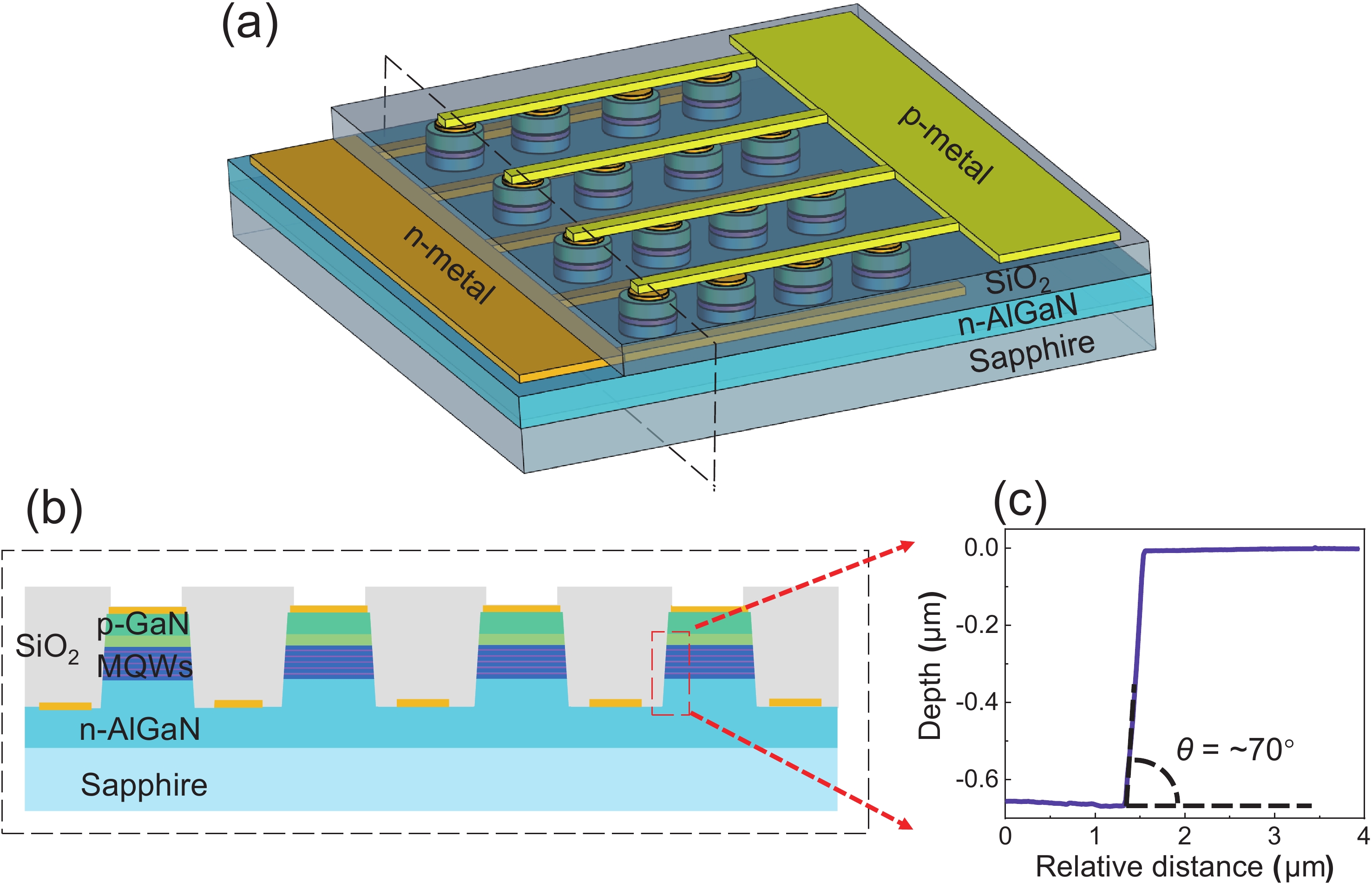
![]()
Figure 1.(Color online) (a) Schematic of a fabricated DUV
The inclination angle of the sidewalls is around 70° which is characterized by the atomic force microscopy (AFM), as shown in Fig. 1(c). The electroluminescence (EL) spectra, the light output power, and the far-field emission for all the fabricated devices were measured from the back of the sapphire (not the epi-side) at room temperature. The far-field emission distribution of the LEDs was recorded by measuring the radiant intensity in angular steps of 10° on a three-axes rotation stage using a power meter at a distance of 50 mm from the LED chips.
3. Results and discussions
The current–voltage (I–V) curves for all the three investigated DUV LEDs are illustrated in Fig. 2(a). The forward voltages for the μ-LED array (50 μm) and the μ-LED array (20 μm) are slightly lower than that for the C-LED, as a result of the lower series resistance in the parallel device configuration and different n- contact areas. The inset of Fig. 2(a) shows the logarithmic plot of the forward I–V curves. The reverse bias leakage values were as low as ~0.1 pA at an applied voltage of –4 V, showing the high quality of the as-grown epi-films and the low damage of the device during the dry-etching process. Notably, the μ-LED array has a minor increase of leakage current than that of the C-LED, which could be attributed to the sidewall defects that may act as the current leakage pathways[
![]()
Figure 2.(Color online) (a) The current–voltage (
As shown in Fig. 3(a), the μ-LED array (50 μm) and the μ-LED array (20 μm) exhibit a higher LOP by 34% and 52% than that of the C-LED under the injected current level of 100 mA, respectively. Notably, the LOP of the device gradually increases with the increased injection current, but the LOP of C-LED reaches the maximum value at about 100 mA (the injected current density of 318 A/cm2) owing to the current injection saturation. Importantly, the μ-LED array can sustain a much higher current injection. In the μ-LED array, since the μ-LEDs are interconnected in parallel, each μ-LED is only injected several milliamperes under the total injection current of 100 mA, which is far from the current saturation. Therefore, the enhanced LOP leads to a significant higher EQE by 34% for the μ-LED array (50 μm) and by 52% for the μ-LED array (20 μm) at 100 mA, as displayed in Fig. 3(b). The peak EQE is 7% and 22% higher in the μ-LED array (50 μm) and μ-LED array (20 μm), respectively, in comparison to that of the C-LED. We also quantify the EQE droop levels at the injection current of 100 mA (the droop is defined as from the highest to the lowest), which are 47.2%, 34.6%, and 34.1% for the C-LED, the μ-LED array (50 μm), and the μ-LED array (20 μm), respectively. Then, the WPE values of the LEDs can be calculated from LOP measurements by[
![]()
Figure 3.(Color online) (a) The light output power (LOP), (b) the external quantum efficiency (EQE), (c) the wall-plug efficiency, and (d) the LEE enhancement factor of the DUV LEDs at different currents for the three investigated devices.
From the calculation results shown in Fig. 3(c), the μ-LED array (50 μm) has higher WPE by 40%, and μ-LED array (20 μm) has higher WPE by 57% at 100 mA than that of the C-LED. This improvement is slightly larger than the EQE enhancement at 100 mA (34% for μ-LED array (50 μm) and 52% for μ-LED array (20 μm)), due to the possible higher current injection efficiency (CIE) in the μ-LED array configuration. Nevertheless, it can be explained that the enhancement of the WPE mainly lies in the effective improvement of EQE since all three LEDs have the same internal quantum efficiency (IQE) as they are fabricated on the same wafer. Therefore, there are ample reasons to explain that the enhancement of the LOP, EQE, and WPE is mainly attributed to the improvement of LEE. Furthermore, Fig. 3(d) shows the LEE enhancement factor[
To further reveal the underlying mechanism of the optical performance enhancement for the DUV μ-LED array, we further use FDTD simulation to analyze the LEEs for C-LED and the μ-LED arrays. In the simulation, a single dipole that served as the radiation source for the LED is located in the middle of the MQW layer[
As an example, the electric field distributions for the DUV μ-LED (20 μm) are shown in Figs. 4(a) and 4(b). It can be observed that more DUV photons have been reflected on the sapphire side as the dipole source moves to the edge of the inclined sidewall. Furthermore, as shown in Figs. 4(c) and 4(d), it can be found that the LEEs of TM- and TE-polarized light increase as the dipole source moves to the mesa edge. Hence, we may conclude that the enhanced LEE of the μ-LED is mainly benefitting from an enlarged ration of the sidewall area to the emission area. The smaller the device is, the larger the ratio becomes, which promotes higher LEE eventually.
![]()
Figure 4.(Color online) Electric field distributions for the light propagation paths of the TM-polarized light when the dipole source at (a) the center of the mesa and (b) the edge of the mesa. The LEEs for the (c) TE- and (d) TM-polarized light as a function of the position of the dipole source for the C-LED,
Additionally, we also recorded the far-field radiation pattern of the C-LED, the μ-LED array (50 μm), and the μ-LED array (20 μm) at the injection current of 100 mA, which are presented in Fig. 5(a). A significantly stronger extracted light intensity was observed for the array over the entire angular radiation range compared with that of the C-LED. The μ-LED array (20 μm) shows the highest light intensity. The spatial light intensities of all three samples reached to the maximum values at the emission angle of 0° when the devices were working at 100 mA. In Fig. 5(b), the divergence angle of the far-field patterns, extracted from Fig. 5(a), are 113.4°, 110.3°, and 108.7°, for the C-LED, the μ-LED array (50 μm), and the μ-LED array (20 μm), respectively. To better explain the phenomenon, schematic illustrations of light propagation characteristic in the C-LED and the μ-LED array are exhibited in Figs. 5(c) and 5(d). In the C-LED, the severe TIR would block the downward-traveling DUV photons inside the device; meanwhile, the lateral-traveling DUV photons would be re-absorbed within a travel distance of ~15 μm[
![]()
Figure 5.(Color online) (a) Far-field patterns for the C-LED, the
4. Conclusion
In summary, we have performed a systematic investigation on the electrical and optical performance of the DUV μ-LED array. Compared with the C-LED, the DUV μ-LED array (20 μm) shows a larger LOP by 52% at 100 mA with a higher peak EQE by 22% and a narrower divergence angle. Moreover, through the numerical analysis, it has been verified that the enlarged LEE for the μ-LED array is attributed to an enhanced light reflection at the sidewall along with the shortened lateral propagation distance of photons. Hence, the DUV μ-LED array with a smaller pixel size should exhibit better optical performance owing to the higher LEE. With an even smaller size (for example, 10 μm), a much higher LEE could be expected. Also, the light propagates with better directionality in the μ-LED array. These observations offer a comprehensive understanding of the optical behavior in the μ-LED array, which can help the community to build high-efficiency and high-power DUV LEDs for various applications.
Acknowledgements
This work was funded by the National Natural Science Foundation of China (Grant Nos. 52161145404, 61905236, 51961145110), the Fundamental Research Funds for the Central Universities (Grant No. WK2100230020), USTC Research Funds of the Double First-Class Initiative (Grant No. YD3480002002), and was partially carried out at the USTC Center for Micro and Nanoscale Research and Fabrication.
References
[1] H C Zhang, C Huang, K Song et al. Compositionally graded III-nitride alloys: Building blocks for efficient ultraviolet optoelectronics and power electronics. Rep Prog Phys, 84, 044401(2021).
[2] M Kneissl, T Y Seong, J Han et al. The emergence and prospects of deep-ultraviolet light-emitting diode technologies. Nat Photonics, 13, 233(2019).
[3] H Inagaki, A Saito, H Sugiyama et al. Rapid inactivation of SARS-CoV-2 with deep-UV LED irradiation. Emerg Microbes Infect, 9, 1744(2020).
[4] Z J Ren, H B Yu, Z L Liu et al. Band engineering of III-nitride-based deep-ultraviolet light-emitting diodes: A review. J Phys D, 53, 073002(2020).
[5] M Guttmann, A Susilo, L Sulmoni et al. Light extraction efficiency and internal quantum efficiency of fully UVC-transparent AlGaN based LEDs. J Phys D, 54, 335101(2021).
[6] Z H Zheng, Q Chen, J N Dai et al. Enhanced light extraction efficiency via double nano-pattern arrays for high-efficiency deep UV LEDs. Opt Laser Technol, 143, 107360(2021).
[7] J Zhang, H P Zhao, N. Tansu. Effect of crystal-field split-off hole and heavy-hole bands crossover on gain characteristics of high Al-content AlGaN quantum well lasers. Appl Phys Lett, 97, 111105(2010).
[8] R Floyd, K Hussain, A Mamun et al. Photonics integrated circuits using Al
[9] X C Peng, W Guo, H Q Xu et al. Significantly boosted external quantum efficiency of AlGaN-based DUV-LED utilizing thermal annealed Ni/Al reflective electrodes. Appl Phys Express, 14, 072005(2021).
[10] S Zhou, X Liu, Y Gao et al. Numerical and experimental investigation of GaN-based flip-chip light-emitting diodes with highly reflective Ag/TiW and ITO/DBR Ohmic contacts. Opt Express, 25, 26615(2017).
[11] Y Zheng, Y Zhang, J Zhang et al. Effects of meshed p-type contact structure on the light extraction effect for deep ultraviolet flip-chip light-emitting diodes. Nanoscale Res Lett, 14, 149(2019).
[12] G Zhang, H Shao, M Y Zhang et al. Enhancing the light extraction efficiency for AlGaN-based DUV LEDs with a laterally over-etched p-GaN layer at the top of truncated cones. Opt Express, 29, 30532(2021).
[13] W Shin, A Pandey, X Liu et al. Photonic crystal tunnel junction deep ultraviolet light emitting diodes with enhanced light extraction efficiency. Opt Express, 27, 38413(2019).
[14] R L Liang, J N Dai, L L Xu et al. High light extraction efficiency of deep ultraviolet LEDs enhanced using nanolens arrays. IEEE Trans Electron Devices, 65, 2498(2018).
[15] S I Inoue, T Naoki, T Kinoshita et al. Light extraction enhancement of 265 nm deep-ultraviolet light-emitting diodes with over 90 mW output power via an AlN hybrid nanostructure. Appl Phys Lett, 106, 131104(2015).
[16] Y K Ooi, J Zhang. Light extraction efficiency analysis of flip-chip ultraviolet light-emitting diodes with patterned sapphire substrate. IEEE Photonics J, 10, 1(2018).
[17] P Manley, S Walde, S Hagedorn et al. Nanopatterned sapphire substrates in deep-UV LEDs: Is there an optical benefit. Opt Express, 28, 3619(2020).
[18] H Yu, H Jia, Z Liu et al. Development of highly efficient ultraviolet LEDs on hybrid patterned sapphire substrates. Opt Lett, 46, 5356(2021).
[19] H P Hu, B Tang, H Wan et al. Boosted ultraviolet electroluminescence of InGaN/AlGaN quantum structures grown on high-index contrast patterned sapphire with silica array. Nano Energy, 69, 104427(2020).
[20] C Zhang, N Tang, L L Shang et al. Local surface plasmon enhanced polarization and internal quantum efficiency of deep ultraviolet emissions from AlGaN-based quantum wells. Sci Rep, 7, 2358(2017).
[21] S J Zhou, H H Xu, B Tang et al. High-power and reliable GaN-based vertical light-emitting diodes on 4-inch silicon substrate. Opt Express, 27, A1506(2019).
[22] Q Chen, H X Zhang, J N Dai et al. Enhanced the optical power of AlGaN-based deep ultraviolet light-emitting diode by optimizing mesa sidewall angle. IEEE Photonics J, 10, 1(2018).
[23] J W Lee, J H Park, D Y Kim et al. Arrays of truncated cone AlGaN deep-ultraviolet light-emitting diodes facilitating efficient outcoupling of in-plane emission. ACS Photonics, 3, 2030(2016).
[24] J Zhang, L Chang, Y Zheng et al. Integrating remote reflector and air cavity into inclined sidewalls to enhance the light extraction efficiency for AlGaN-based DUV LEDs. Opt Express, 28, 17035(2020).
[25] M Tian, H Yu, M H Memon et al. Enhanced light extraction of the deep-ultraviolet micro-LED via rational design of chip sidewall. Opt Lett, 46, 4809(2021).
[26] H Yu, M H Memon, D Wang et al. AlGaN-based deep ultraviolet micro-LED emitting at 275 nm. Opt Lett, 46, 3271(2021).
[27] R Floyd, M Gaevski, K Hussain et al. Enhanced light extraction efficiency of micropixel geometry AlGaN DUV light-emitting diodes. Appl Phys Express, 14, 084002(2021).
[28] R Floyd, M Gaevski, M D Alam et al. An opto-thermal study of high brightness 280 nm emission AlGaN micropixel light-emitting diode arrays. Appl Phys Express, 14, 014002(2021).
[29] R T Ley, J M Smith, M S Wong et al. Revealing the importance of light extraction efficiency in InGaN/GaN microLEDs via chemical treatment and dielectric passivation. Appl Phys Lett, 116, 251104(2020).
[30] S Zhang, Y Liu, J Zhang et al. Optical polarization characteristics and light extraction behavior of deep-ultraviolet LED flip-chip with full-spatial omnidirectional reflector system. Opt Express, 27, A1601(2019).
[31] T B Wei, K Wu, D Lan et al. Selectively grown photonic crystal structures for high efficiency InGaN emitting diodes using nanospherical-lens lithography. Appl Phys Lett, 101, 211111(2012).


Set citation alerts for the article
Please enter your email address

© Copyright 2018-2021 | Chinese Laser Press. All Rights Reserved 沪ICP备15018463号-20