• Journal of Semiconductors
  • Vol. 41, Issue 11, 111405 (2020)
Mo Huang1, Yan Lu1, and Rui P. Martins1、2
Author Affiliations
  • 1State Key Laboratory of Analog and Mixed-Signal VLSI, Institute of Microelectronics, DECE/FST, University of Macau, Macau, China
  • 2On leave from the Instituto Superior Técnico, Universidade de Lisboa, Lisbon, 1049-001, Portugal
  • show less
    DOI: 10.1088/1674-4926/41/11/111405 Cite this Article
    Mo Huang, Yan Lu, Rui P. Martins. A comparative study of digital low dropout regulators[J]. Journal of Semiconductors, 2020, 41(11): 111405 Copy Citation Text show less
    (Color online) Granular power management in an SoC.
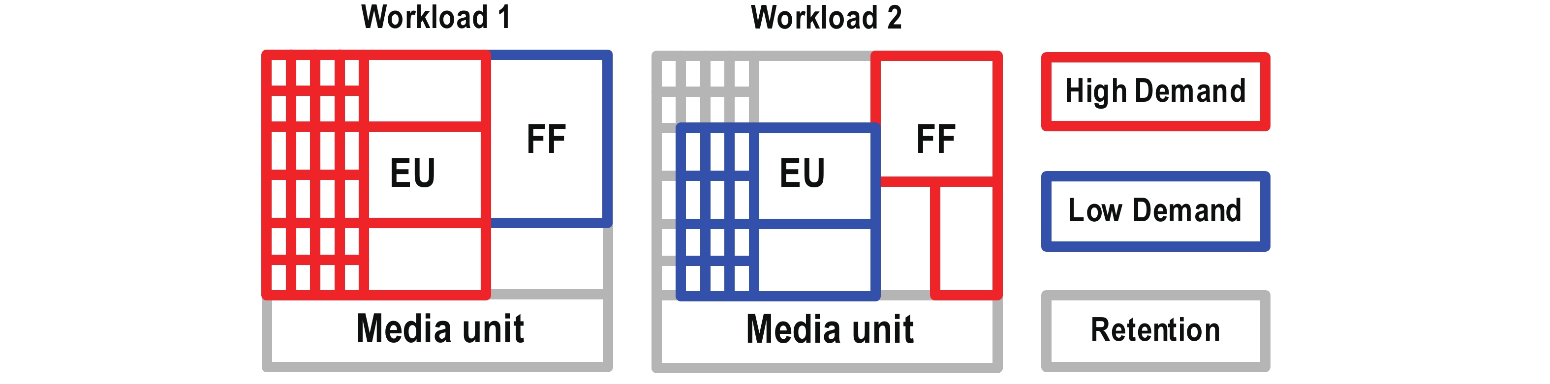
    Fig. 1. (Color online) Granular power management in an SoC.
    (Color online) DLDO requirements in an SoC.
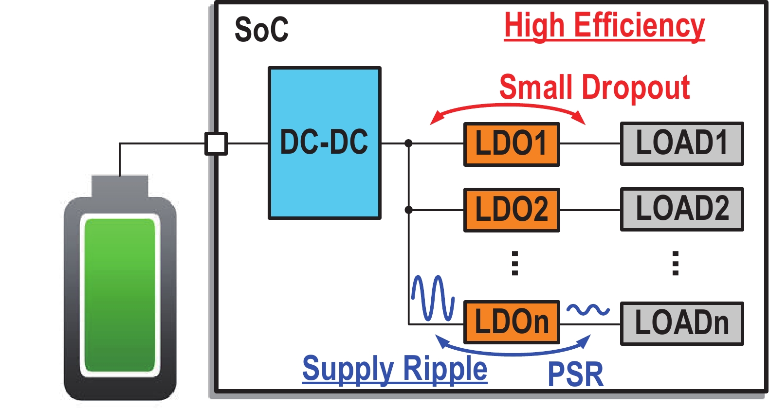
    Fig. 2. (Color online) DLDO requirements in an SoC.
    Block diagram of (a) ALDO and (b) DLDO.
    Fig. 3. Block diagram of (a) ALDO and (b) DLDO.
    (Color online) The output voltage undershoot analysis of DLDO.
    Fig. 4. (Color online) The output voltage undershoot analysis of DLDO.
    (a) Measured LCO of DLDO, (b) small-signal model of DLDO, and (c) root locus of 2-level quantized DLDO.
    Fig. 5. (a) Measured LCO of DLDO, (b) small-signal model of DLDO, and (c) root locus of 2-level quantized DLDO.
    (Color online) Power supply rejection process of a conventional DLDO.
    Fig. 6. (Color online) Power supply rejection process of a conventional DLDO.
    Latch-based comparator.
    Fig. 7. Latch-based comparator.
    Continuous multi-bit quantizer based on (a) current-mirror and (b) inverter.
    Fig. 8. Continuous multi-bit quantizer based on (a) current-mirror and (b) inverter.
    DLDO based on a VCO quantizer.
    Fig. 9. DLDO based on a VCO quantizer.
    (Color online) Output voltage transient response under I-only, P-only, PI, and PID control.
    Fig. 10. (Color online) Output voltage transient response under I-only, P-only, PI, and PID control.
    Change CLK when VOUT exceeds the VREF window.
    Fig. 11. Change CLK when VOUT exceeds the VREF window.
    (Color online) Analog-assisted loop in (a)[15–17], (b)[18], and (c)[31].
    Fig. 12. (Color online) Analog-assisted loop in (a)[1517], (b)[18], and (c)[31].
    (a) Analog circuits help PSR improvement and (b) block diagram of the hybrid LDO.
    Fig. 13. (a) Analog circuits help PSR improvement and (b) block diagram of the hybrid LDO.
    Improving PSR using (a) feedforward PSR cancellation[33] and (b) replica loop[34, 35].
    Fig. 14. Improving PSR using (a) feedforward PSR cancellation[33] and (b) replica loop[34, 35].
    (Color online) Simulated PSRs of the conventional DLDO, hybrid LDOs without replica loop, and with replica loop.
    Fig. 15. (Color online) Simulated PSRs of the conventional DLDO, hybrid LDOs without replica loop, and with replica loop.
    (Color online) Multi-LDOs assisting a neighboring load step.
    Fig. 16. (Color online) Multi-LDOs assisting a neighboring load step.
    TypeContinuous SensingSpeedPower ConsumptionRobustness
    Single-bitNoFastLowHigh
    Multi-bitCurrent-to-code ADC[21]YesFastHighHigh
    Flash ADC[22]YesFastHighHigh
    TDC[23]YesFastMediumNeed calibration
    VCO+PD[24, 25]YesSlow (1/s effect)MediumHigh
    Table 1. Features of the quantizers in DLDO design.
    YearProcess (nm)ArchitectureFoM (ps)
    2020[39]130ADC + PID63.9
    2016[22]65ADC + Event driven20
    2016[21]28ADC + Coarse/fine9.57
    2020[40]20ADC + Computational6.7
    2020[36]10TDC + PID5.2
    2017[15]65Analog-assisted0.23
    2018[18]28Analog-assisted0.026
    Table 2. FoM of speed versus process nodes.
    Mo Huang, Yan Lu, Rui P. Martins. A comparative study of digital low dropout regulators[J]. Journal of Semiconductors, 2020, 41(11): 111405
    Download Citation