
Qiang Gao, Hasan Sahin, Jun Kang. Strain tunable band structure of a new 2D carbon allotrope C568[J]. Journal of Semiconductors, 2020, 41(8): 082005
- Journal of Semiconductors
- Vol. 41, Issue 8, 082005 (2020)
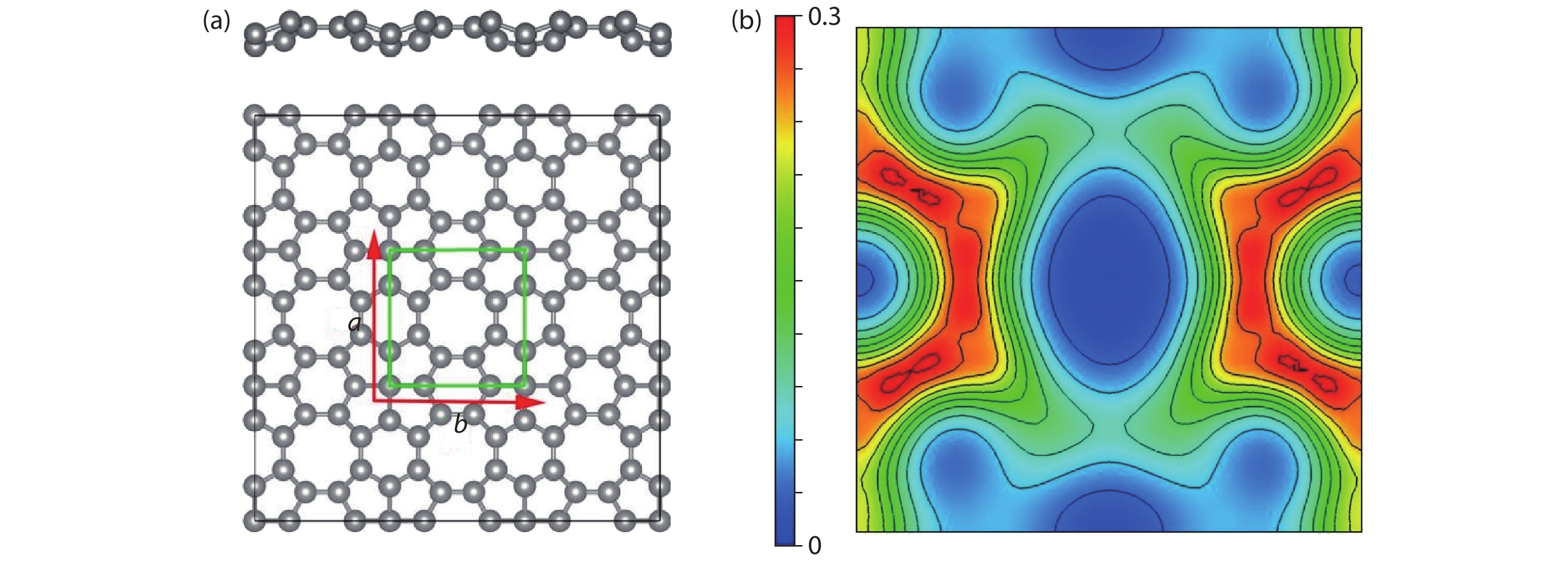
Fig. 1. (Color online) (a) The crystalline structures and (b) 2D charge density difference plot of C568. The square unit-cell marked in green line, where a and b represent unitcell vectors.
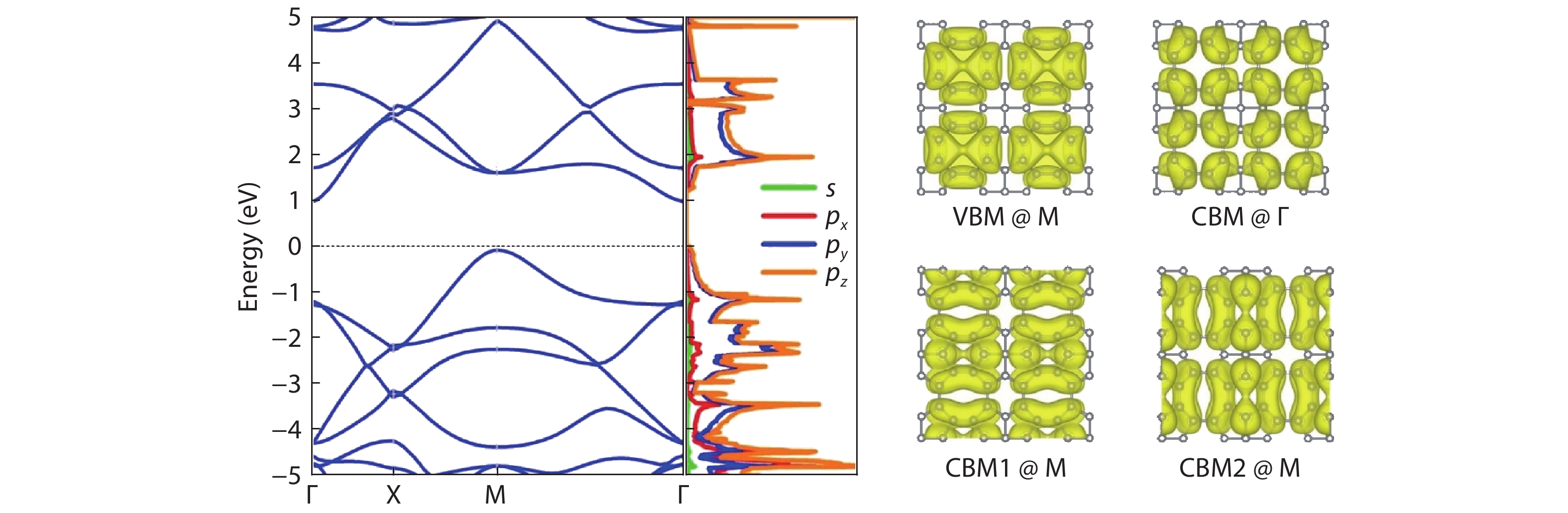
Fig. 2. (Color online) The band structures and projected density of states of C568, with the Fermi level are set to zero. The charge densities of several key states are also presented.
Fig. 3. (Color online) Band structures of C568 with different uniaxial strains, with the Fermi level set at zero and marked with the black dashed line. Positive and negative values of strains indicate tensile and compressive cases, respectively.
Fig. 4. (Color online) (a) Band gap, (b) band edge position, (c) optical absorption, and (d) effective mass of C568 with different uniaxial strains. CBM_Γ and CBM_M are the conduction band minimum at Γ and M points. The vacuum level is taken as the zero energy reference in (b).
Fig. 5. (Color online) Band structures of C568 with different biaxial strains, with the Fermi level set at zero and marked with blacked dashed line. Positive and negative values of strains indicate tensile and compressive cases, respectively.
Fig. 6. (Color online) (a) Band gap, (b) band alignment, (c) optical absorption, and (d) effective mass of C568 with different biaxial strains. CBM_Γ and CBM_M are the conduction band minimum at Γ and M points. The vacuum level is taken as the zero-energy reference in (b).

Set citation alerts for the article
Please enter your email address
© Copyright 2018-2021 | Chinese Laser Press. All Rights Reserved 沪ICP备15018463号-20