
Qiang Gao, Hasan Sahin, Jun Kang. Strain tunable band structure of a new 2D carbon allotrope C568[J]. Journal of Semiconductors, 2020, 41(8): 082005
- Journal of Semiconductors
- Vol. 41, Issue 8, 082005 (2020)
Abstract
1. Introduction
The success of graphene have triggered the tide of searching novel two-dimensional (2D) materials with desired properties[
Recently, a new 2D carbon allotrope named C568 has been predicted, which is composed of 5, 6, and 8-membered rings of carbon[
2. Computational methods
The electronic structures of C568 are calculated through density functional theory, which is realized in the Vienna abinitio Simulation Package (VASP)[
3. Results and discussion
3.1. The crystalline structure and electronic structures of C568
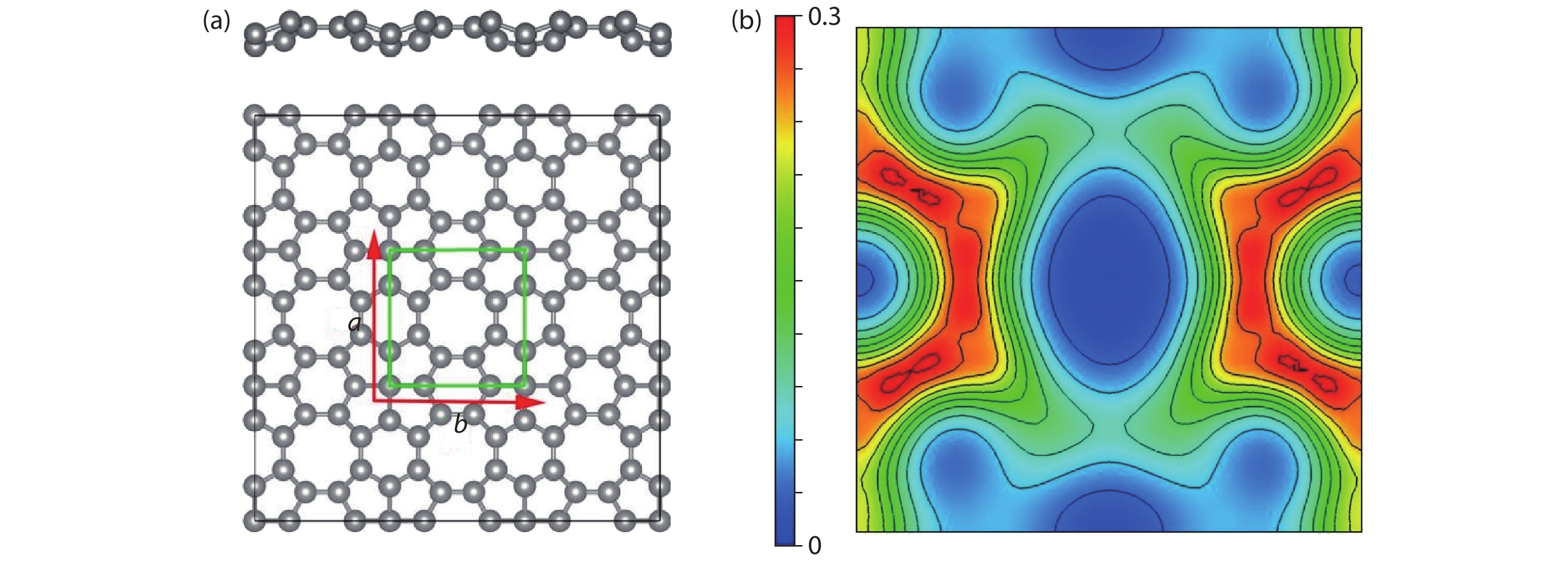
To study the electronic structures of C568, the crystalline structure of C568 has been optimized (Fig. 1(a)).
As seen, C568 is formed of 5-, 6-, and 8-membered rings, which are composed of sp2- and sp3-hybridized carbon atoms. Different from sp2 hybridized graphene, the carbon rings in C568 are not in the same plane, due to the presence of sp3-hybridization. C568 possesses a space group of P-4m2(115) with tetragonal lattice. The optimized C568 unit cell contains 13 carbon atoms with lattice parameters of a = b = 5.725 Å, which is consistent with the values reported in a recent work[
The electronic band structure is presented in Fig. 2. The C568 possesses an indirect band structure with a band gap of 1.06 eV, which is consistent with the recent work[
3.2. The external strain effects
External strain is one of the most common effects in the practical applications of materials, which can significantly modify the electronic properties of materials. To understand possible effects of the external strain effect on the electronic properties of C568, we have considered in-plane uniaxial strain and biaxial strain. Through calculations, three unique properties have been found: 1) an indirect-to-direct band gap transition occurs under compressive strain; 2) uniaxial strain and biaxial strain have different effects on the band gap of C568; and 3) uniaxial can induce large optical anisotropy, while biaxial strain cannot. In the following sections, these findings are discussed in detail.
The uniaxial strain effect is firstly studied. The electronic band structures with different strain are shown in Fig. 3. When tensile strain is applied, the band structures show indirect character. The locations of the CBM and VBM remain unchanged. Moreover, it can be clearly seen that with increasing tensile strain, the band gap decreases. Under a 10% strain, the band gap is 0.630 eV smaller than that of the equilibrium state. The situation is different when compressive strain is applied. Under a small strain (–2%), the band gap is still indirect. However, when the strain is increased to –6%, the band gap become direct. While the VBM position remains at the M point, the CBM changes from the Γ to the M point. When compressive strain is further enhanced, the direct band structures are still kept. For the direct band gap, the optical transition between VBM and CBM becomes efficient. Electrons can be excited from VBM to CBM without the assistance of lattice phonons, which is very beneficial to the optoelectronic applications. To clearly show the change of band gap, in Fig. 4, we present the evolution of band gap with external uniaxial strain. It can be seen that the band gap of C568 decreases with the increasing tensile strain, and the indirect character is preserved. When compressive strain increase from 0 to –4%, the band gap increases, however, it begins to decrease when the compressive strain exceeds –4%, and becomes direct as discussed above.
The transition from the indirect to direct band gap can be understood from the change of band edge positions at different k points with the applications of strain, as shown in Fig. 4(b). The absolute band edge position is calculated through setting the vacuum level (Evac) as the zero energy reference of calculation[
The difference responses lead to a crossover for the CBM_M and CBM_Γ when the compressive strain increases to –4%. Thus, the indirect band structures transform to direct. Moreover, under compressive strain, due to the energy decrease of the CBM_M state, the band gap value decreases when compressive strain is at the range of –4% to –10%.
The optical anisotropy is also a critical factor in design of polarized optoelectronic devices[
In the following part, the effect of biaxial strain is investigated. We have firstly calculated the band structures of C568 with different biaxial strain, which are shown in Fig. 5. For the case of tensile strain, the evaluation of band structures is similar to the case of uniaxial strain. The indirect gap character is intact, and the gap value is smaller under larger stain.
For compressive biaxial strain, the band structures show some difference with the case of uniaxial strain. When compressive biaxial strain increases to –6%, the direct band structures can be obtained, with the both CBM and VBM at the M point. When the compressive strain increases to –10%, the direct band structures become indirect again. Another point can be found that the biaxial does not lift the double degeneracy of CBM at the M point. However, in the case of uniaxial strain, the degeneracy is lifted due to the breaking of symmetry along the two lattice vectors. Thus, the optical transition may be different in the case of uniaxial and biaxial strain.
In Fig. 6, we have also calculated the band gap with different biaxial strain. It can be seen that the change of band gap is different from the case of uniaxial strain. When tensile strain is exerted to C568, the band gap keeps dropping. As the tensile strain is enlarged from 0 to 10%, the band gap decreases from 1.062 to 0.380 eV. The trend is the same in the case of uniaxial strain.
However, applying compressive strain from 0 to –10% can make the band gap increase from 1.062 to 1.612 eV, which is different from the case of uniaxial strain. However, applying compressive strain from 0 to –10% can make the band gap increase from 1.062 to 1.612 eV, which is different from the case of uniaxial strain. The tunable range of band gap is 0.381–1.612 eV, which can cover the near-infrared region and visible light region. It indicates that, in the experiment, applying biaxial strain can be effective to control the band gap of C568. It is suitable for the design of optoelectronic devices which can work at near-infrared light or visible light. Further, the band gap keeps direct in the strain range of –4% to –9%, which is desired for the optical performance. To understand the transition from indirect to direct band gap, we also calculate the band edge positions, considering the CBM at the M and the Γ points, as well as the VBM at the M point. We can see from Fig. 6(b) that the CBM_M shifts downwards with increasing compressive strain, and becomes lower than CBM_Γ in the range from –4% to –9%, indicating the conduction band minimum changes from the M to the Γ points. The downward shift is also consistent with the bonding character of CBM_M. Thus, the direct band gap is formed. In addition, in the direct gap region the VBM also shift down with a slightly larger rate compared with the CBM_M, resulting in the tiny increase of the band gap value with enhanced strain. The optical absorption for C568 with the strain of –6% is also calculated in Fig. 6(c). The results show that the absorption is isotropic along the x and y direction, which is different from the optical anisotropy in case of uniaxial strain. It is because uniaxial strain makes the lattice become rectangle. Compared to the square lattice caused by biaxial strain, the lattice symmetry decreases in the rectangle lattice. The decrease of lattice symmetry along x and y direction renders the optical anisotropy along x and y direction. The effective mass of hole and electron with the external biaxial strain is also calculated (see Fig. 6(d)). Compared to the effective mass with uniaxial strain, the effective mass for electron and hole is relatively larger.
In experiments, some flexible materials can be the ideal substrate for the growth of 2D C568, such as graphene and plastic substrates. Compressive and tensile strains can be applied on C568 by twisting and stretching the substrate. Previous works show that using flexible PVA substrate to encapsulate monolayer 2D material, and twisting soft polymeric substrates with materials are practical ways to modulate the electronic properties of materials and design flexible devices[
4. Conclusion
Through first-principle calculations, the effect of the external strain on the electronic properties of C568 have been investigated theoretically. The calculations show that while in-plane uniaxial and biaxial strains both reduces the band gap of C568 in case of tensile strain, their effects are quite different in case of compressive strain. With increasing compressive uniaxial strain, the band gap of C568 first increases, and then dramatically decreases. In contrast, the application of compressive biaxial strain up to –10% only leads to a slight increase of band gap. Moreover, an indirect-to-direct gap transition can be realized under both types of compressive strain. The results also show that the optical anisotropy of C 568 can be induced under uniaxial strain, while biaxial strain does not cause such an effect. These results could be helpful to experimentally modulate the electronic properties of C568-based nanodevices.
Acknowledgements
This work was supported by NSAF (Grant No. U1930402). Computational resources were provided by Tianhe2-JK at CSRC.
References
[1] K S Novoselov, A K Geim, S V Morozov et al. Two-dimensional gas of massless Dirac fermions in graphene. Nature, 438, 197(2005).
[2] A C Ferrari, J C Meyer, V Scardaci et al. Raman spectrum of graphene and graphene layers. Phys Rev Lett, 97, 187401(2006).
[3] A K Geim, K S Novoselov. The rise of graphene. Nat Mater, 6, 183(2007).
[4] M Y Han, B Özyilmaz, Y B Zhang et al. Energy band-gap engineering of graphene nanoribbons. Phys Rev Lett, 98, 206805(2007).
[5] W J Zhu, D Neumayer, V Perebeinos et al. Silicon nitride gate dielectrics and band gap engineering in graphene layers. Nano Lett, 10, 3572(2010).
[6] K F Mak, C Lee, J Hone et al. Atomically thin MoS2: A new direct-gap semiconductor. Phys Rev Lett, 105, 136805(2010).
[7] B Radisavljevic, A Radenovic, J Brivio et al. Single-layer MoS2 transistors. Nat Nanotechnol, 6, 147(2011).
[8] K F Mak, K He, J Shan et al. Control of valley polarization in monolayer MoS2 by optical helicity. Nat Nanotechnol, 7, 494(2012).
[9] L K Li, Y J Yu, G J Ye et al. Black phosphorus field-effect transistors. Nat Nanotechnol, 9, 372(2014).
[10] E S Reich. Phosphorene excites materials scientists. Nature, 506, 19(2014).
[11] G Fiori, F Bonaccorso, G Iannaccone et al. Erratum: Electronics based on two-dimensional materials. Nat Nanotechnol, 9, 1063(2014).
[12] M S Xu, T Liang, M M Shi et al. Graphene-like two-dimensional materials. Chem Rev, 113, 3766(2013).
[13] P Vogt, P de Padova, C Quaresima et al. Silicene: Compelling experimental evidence for graphenelike two-dimensional silicon. Phys Rev Lett, 108, 155501(2012).
[14] M E Dávila, L Xian, S Cahangirov et al. Germanene: A novel two-dimensional germanium allotrope akin to graphene and silicene. New J Phys, 16, 095002(2014).
[15] F F Zhu, W J Chen, Y Xu et al. Epitaxial growth of two-dimensional stanene. Nat Mater, 14, 1020(2015).
[16] Z Zhu, X Cai, S Yi et al. Multivalency-driven formation of Te-based monolayer materials: A combined first-principles and experimental study. Phys Rev Lett, 119, 106101(2017).
[17] Z H Wang, X F Zhou, X M Zhang et al. Phagraphene: A low-energy graphene allotrope composed of 5-6-7 carbon rings with distorted Dirac cones. Nano Lett, 15, 6182(2015).
[18] Y Liu, G Wang, Q S Huang et al. Structural and electronic properties of
[19] R H Baughman, H Eckhardt, M Kertesz. Structure-property predictions for new planar forms of carbon: Layered phases containing sp2 and sp atoms. J Chem Phys, 87, 6687(1987).
[20] N Narita, S Nagai, S Suzuki et al. Optimized geometries and electronic structures of graphyne and its family. Phys Rev B, 58, 11009(1998).
[21] G X Li, Y L Li, H B Liu et al. Architecture of graphdiyne nanoscale films. Chem Commun, 46, 3256(2010).
[22] M Q Long, L Tang, D Wang et al. Electronic structure and carrier mobility in graphdiyne sheet and nanoribbons: Theoretical predictions. ACS Nano, 5, 2593(2011).
[23] Q Song, B Wang, K Deng et al. Graphenylene, a unique two-dimensional carbon network with nondelocalized cyclohexatriene units. J Mater Chem C, 1, 38(2013).
[24] S H Zhang, J Zhou, Q Wang et al. Penta-graphene: A new carbon allotrope. PNAS, 112, 2372(2015).
[25] B Ram, H Mizuseki. Tetrahexcarbon: A two-dimensional allotrope of carbon. Carbon, 137, 266(2018).
[26] B Ram, H Mizuseki. C568: A new two-dimensional sp2–sp3 hybridized allotrope of carbon. Carbon, 158, 827(2020).
[27] G Kresse, J Furthmüller. Efficient iterative schemes for ab initio total-energy calculations using a plane-wave basis set. Phys Rev B, 54, 11169(1996).
[28] J P Perdew, K Burke, M Ernzerhof. Generalized gradient approximation made simple. Phys Rev Lett, 77, 3865(1996).
[29] P E Blöchl. Projector augmented-wave method. Phys Rev B, 50, 17953(1994).
[30] J Heyd, J E Peralta, G E Scuseria et al. Energy band gaps and lattice parameters evaluated with the Heyd–Scuseria–Ernzerhof screened hybrid functional. J Chem Phys, 123, 174101(2005).
[31] H J Monkhorst, J D Pack. Special points for Brillouin-zone integrations. Phys Rev B, 13, 5188(1976).
[32]
[33] J Kang, S Tongay, J Zhou et al. Band offsets and heterostructures of two-dimensional semiconductors. Appl Phys Lett, 102, 012111(2013).
[34] X Wang, Y Li, L Huang et al. Short-wave near-infrared linear dichroism of two-dimensional germanium selenide. J Am Chem Soc, 139, 14976(2017).
[35] K Zhao, Z M Wei, X W Jiang. Polarized photodetectors based on two-dimensional semiconductors. Sci China Phys Mech Astron, 63, 1(2019).
[36] Z Li, Y Lv, L Ren et al. Efficient strain modulation of 2D materials via polymer encapsulation. Nat Commun, 11, 1151(2020).
[37] D Akinwande, N Petrone, J Hone. Two-dimensional flexible nanoelectronics. Nat Commun, 5, 5678(2014).
[38] S Das, R Gulotty, A V Sumant et al. All two-dimensional, flexible, transparent, and thinnest thin film transistor. Nano Lett, 14, 2861(2014).


Set citation alerts for the article
Please enter your email address

© Copyright 2018-2021 | Chinese Laser Press. All Rights Reserved 沪ICP备15018463号-20