• Acta Physica Sinica
  • Vol. 69, Issue 5, 056101-1 (2020)
Zhan-Gang Zhang1, Zhi-Feng Lei1、*, Teng Tong2, Xiao-Hui Li2, Song-Lin Wang3, Tian-Jiao Liang3, Kai Xi4, Chao Peng1, Yu-Juan He1, Yun Huang1, and Yun-Fei En1
Author Affiliations
  • 1Science and Technology on Reliability Physics and Application of Electronic Component Laboratory, China Electronic Product Reliability and Environmental Testing Research Institute, Guangzhou 510610, China
  • 2Institute of High Energy Physics, Chinese Academy of Sciences, Beijing 100049, China
  • 3Spallation Neutron Source Science Center, Dongguan 523803, China
  • 4Institute of Microelectronics, Chinese Academy of Sciences, Beijing 100029, China
  • show less
    DOI: 10.7498/aps.69.20191209 Cite this Article
    Zhan-Gang Zhang, Zhi-Feng Lei, Teng Tong, Xiao-Hui Li, Song-Lin Wang, Tian-Jiao Liang, Kai Xi, Chao Peng, Yu-Juan He, Yun Huang, Yun-Fei En. Comparison of neutron induced single event upsets in 14 nm FinFET and 65 nm planar static random access memory devices[J]. Acta Physica Sinica, 2020, 69(5): 056101-1 Copy Citation Text show less
    Experimental setup (neutron beam channel is loca-ted behind the test board, and aligned with the device under test).
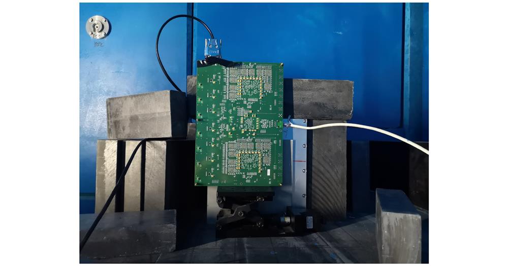
    Fig. 1. Experimental setup (neutron beam channel is loca-ted behind the test board, and aligned with the device under test).
    Neutron energy spectrum of the experimental terminal.
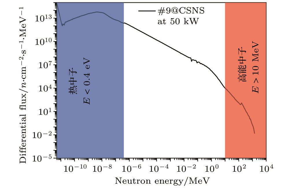
    Fig. 2. Neutron energy spectrum of the experimental terminal.
    Comparison of neutron (E > 10 MeV) SEU cross section of 65 nm planar and 14 nm FinFET SRAM devices.
    Fig. 3. Comparison of neutron (E > 10 MeV) SEU cross section of 65 nm planar and 14 nm FinFET SRAM devices.
    Comparison of thermal neutron SEU cross section of 65 nm planar and 14 nm FinFET SRAM devices.
    Fig. 4. Comparison of thermal neutron SEU cross section of 65 nm planar and 14 nm FinFET SRAM devices.
    Relationship between LET value and energy of (a) Li ion and (b) He ion in silicon material.
    Fig. 5. Relationship between LET value and energy of (a) Li ion and (b) He ion in silicon material.
    Heavy ion experiment results of 14 nm FinFET SRAM.
    Fig. 6. Heavy ion experiment results of 14 nm FinFET SRAM.
    Comparison of neutron MBU ratio of 65 nm planar and 14 nm FinFET SRAM devices (using the full spectrum in Fig. 2).
    Fig. 7. Comparison of neutron MBU ratio of 65 nm planar and 14 nm FinFET SRAM devices (using the full spectrum in Fig. 2).
    Reverse analysis of 14 nm FinFET SRAM: (a) Cross section; (b) memory area image.
    Fig. 8. Reverse analysis of 14 nm FinFET SRAM: (a) Cross section; (b) memory area image.
    Reverse analysis of 65 nm SRAM: (a) Cross section; (b) memory area image.
    Fig. 9. Reverse analysis of 65 nm SRAM: (a) Cross section; (b) memory area image.
    14 MeV and 1600 MeV neutron induced secondary particle distribution in the device SV (W material in the device model is replaced by silica).
    Fig. 10. 14 MeV and 1600 MeV neutron induced secondary particle distribution in the device SV (W material in the device model is replaced by silica).
    14 MeV and 1600 MeV neutron induced secondary particle distribution in the device SV (real device model).
    Fig. 11. 14 MeV and 1600 MeV neutron induced secondary particle distribution in the device SV (real device model).
    The LET value and range of secondary particles generated by 14 MeV and 1600 MeV neutrons in the device SV.
    Fig. 12. The LET value and range of secondary particles generated by 14 MeV and 1600 MeV neutrons in the device SV.
    The deposition charge of 14 MeV and 1600 MeV neutrons in the device SV.
    Fig. 13. The deposition charge of 14 MeV and 1600 MeV neutrons in the device SV.
    编号SRAM工艺型号容量供电电压(core)/V封装形式
    1#65 nm平面CY7 C1663 KV188 Mb × 181.8BGA, 非倒装
    2#14 nm FinFET8 Mb × 160.8BGA, 倒装
    Table 1.

    Parameters of devices under test.

    被测器件参数

    器件存储单元尺寸/ μm × μm 灵敏区尺寸/ μm × μm 灵敏区厚度/nm重离子LET阈值/ MeV·cm2·mg–1临界电荷/fC
    14 nm FinFET SRAM0.37 × 0.180.08 × 0.03450.10.05
    65 nm SRAM1.0 × 0.50.20 × 0.194500.22 [18]1[19]
    Table 2.

    Memory cell size and SV parameters for the 14 nm FinFET SRAM and 65 nm SRAM devices.

    14 nm FinFET SRAM和65 nm SRAM的存储单元尺寸和灵敏区参数

    Zhan-Gang Zhang, Zhi-Feng Lei, Teng Tong, Xiao-Hui Li, Song-Lin Wang, Tian-Jiao Liang, Kai Xi, Chao Peng, Yu-Juan He, Yun Huang, Yun-Fei En. Comparison of neutron induced single event upsets in 14 nm FinFET and 65 nm planar static random access memory devices[J]. Acta Physica Sinica, 2020, 69(5): 056101-1
    Download Citation