• Journal of Semiconductors
  • Vol. 43, Issue 8, 082802 (2022)
Lixin Tian1、*, Zechen Du1, Rui Liu1, Xiping Niu1, Wenting Zhang1, Yunlai An1, Zhanwei Shen2, Fei Yang1、**, and Xiaoguang Wei1
Author Affiliations
  • 1State Key Laboratory of Advanced Power Transmission Technology, Global Energy Interconnection Research Institute Co., Ltd., Beijing 102209, China
  • 2Key Laboratory of Semiconductor Material Sciences, Institute of Semiconductors, Chinese Academy of Sciences, Beijing 100083, China
  • show less
    DOI: 10.1088/1674-4926/43/8/082802 Cite this Article
    Lixin Tian, Zechen Du, Rui Liu, Xiping Niu, Wenting Zhang, Yunlai An, Zhanwei Shen, Fei Yang, Xiaoguang Wei. Influence of epitaxial layer structure and cell structure on electrical performance of 6.5 kV SiC MOSFET[J]. Journal of Semiconductors, 2022, 43(8): 082802 Copy Citation Text show less
    (Color online) Current density and blocking voltage variation with doping concentration and thickness of epitaxial layer.
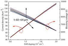
    Fig. 1. (Color online) Current density and blocking voltage variation with doping concentration and thickness of epitaxial layer.
    (Color online) Schematic cross-section of 6.5 kV SiC MOSFET.
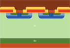
    Fig. 2. (Color online) Schematic cross-section of 6.5 kV SiC MOSFET.
    (Color online) 6.5 kV SiC MOSFET devices on the 6-inch wafer.
    Fig. 3. (Color online) 6.5 kV SiC MOSFET devices on the 6-inch wafer.
    (Color online) Comparison of output current of five chips on three wafers.
    Fig. 4. (Color online) Comparison of output current of five chips on three wafers.
    (Color online) Comparison of output, transfer and derivative parameters of five cell structures. (a) Output characteristic curves. (b) Transfer characteristic curves. (c) Transconductance comparison of different channel lengths. (d) Cell transconductance comparison of different JFET widths.
    Fig. 5. (Color online) Comparison of output, transfer and derivative parameters of five cell structures. (a) Output characteristic curves. (b) Transfer characteristic curves. (c) Transconductance comparison of different channel lengths. (d) Cell transconductance comparison of different JFET widths.
    (Color online) Breakdown characteristics of test pattern gate oxide capacitors.
    Fig. 6. (Color online) Breakdown characteristics of test pattern gate oxide capacitors.
    (Color online) The transforming curves of the gate oxide capacitor I–V curves.
    Fig. 7. (Color online) The transforming curves of the gate oxide capacitor I–V curves.
    (Color online) The relationship between barrier height and slope.
    Fig. 8. (Color online) The relationship between barrier height and slope.
    (Color online) 6.5 kV SiC MOSFET package layout and outline.
    Fig. 9. (Color online) 6.5 kV SiC MOSFET package layout and outline.
    High temperature gate bias reliability. (a) Forward gate voltage test results. (b) Reverse gate voltage test results.
    Fig. 10. High temperature gate bias reliability. (a) Forward gate voltage test results. (b) Reverse gate voltage test results.
    The results of high temperature reverse bias reliability.
    Fig. 11. The results of high temperature reverse bias reliability.
    #1#2#3
    C136.36%54.55%61.90%
    C236.36%54.55%57.14%
    C340.91%54.55%38.10%
    C431.82%50.00%42.86%
    C554.55%63.64%52.38%
    Table 0. Chip yield of 3 wafers.
    Cell numberChannel length (μm) Width of JFET region (μm)
    C10.754
    C21.254
    C314
    C413
    C515
    Table 0. Cell parameter table.
    NumberThickness (μm) Doping (1015cm−3) t/( Ndqμ)
    #164.71.2934.1
    #262.31.1636.5
    #362.51.2234.8
    Table 0. Epitaxial layer thickness and doping concentration.
    Lixin Tian, Zechen Du, Rui Liu, Xiping Niu, Wenting Zhang, Yunlai An, Zhanwei Shen, Fei Yang, Xiaoguang Wei. Influence of epitaxial layer structure and cell structure on electrical performance of 6.5 kV SiC MOSFET[J]. Journal of Semiconductors, 2022, 43(8): 082802
    Download Citation