Lixin Tian, Zechen Du, Rui Liu, Xiping Niu, Wenting Zhang, Yunlai An, Zhanwei Shen, Fei Yang, Xiaoguang Wei. Influence of epitaxial layer structure and cell structure on electrical performance of 6.5 kV SiC MOSFET[J]. Journal of Semiconductors, 2022, 43(8): 082802
Copy Citation Text
Silicon carbide (SiC) material features a wide bandgap and high critical breakdown field intensity. It also plays an important role in the high efficiency and miniaturization of power electronic equipment. It is an ideal choice for new power electronic devices, especially in smart grids and high-speed trains. In the medium and high voltage fields, SiC devices with a blocking voltage of more than 6.5 kV will have a wide range of applications. In this paper, we study the influence of epitaxial material properties on the static characteristics of 6.5 kV SiC MOSFET. 6.5 kV SiC MOSFETs with different channel lengths and JFET region widths are manufactured on three wafers and analyzed. The FN tunneling of gate oxide, HTGB and HTRB tests are performed and provide data support for the industrialization process for medium/high voltage SiC MOSFETs.Silicon carbide (SiC) material features a wide bandgap and high critical breakdown field intensity. It also plays an important role in the high efficiency and miniaturization of power electronic equipment. It is an ideal choice for new power electronic devices, especially in smart grids and high-speed trains. In the medium and high voltage fields, SiC devices with a blocking voltage of more than 6.5 kV will have a wide range of applications. In this paper, we study the influence of epitaxial material properties on the static characteristics of 6.5 kV SiC MOSFET. 6.5 kV SiC MOSFETs with different channel lengths and JFET region widths are manufactured on three wafers and analyzed. The FN tunneling of gate oxide, HTGB and HTRB tests are performed and provide data support for the industrialization process for medium/high voltage SiC MOSFETs.
1. Introduction
Silicon carbide (SiC) is a typical representative of the wide bandgap of semiconductors, due to its bandgap, strong critical breakdown field and high thermal conductivity. SiC materials and devices have been included in the National 14th Five-Year Plan for Science and Technology[1, 2]. In the past two decades, SiC power devices have been widely used in low-voltage applications. Companies such as CREE[3], Rohm[4], and Infineon[5] have dominated the market. In high-voltage applications, SiC devices have been used in high-speed motor drives, solid-state transformers, railway traction and fast chargers for electric vehicles[6-8]. In traditional silicon-based power converters, high-voltage silicon IGBTs are usually connected in parallel and in series to meet the needs of high voltage and high current. However, series and parallel connections will introduce voltage imbalance and current imbalance, respectively.
High voltage devices play a significant role in improving device performance and equipment reliability[9]. Silicon carbide metal–oxide–semiconductor field effect transistors (SiC MOSFETs) have the advantages of high voltage, low loss, high temperature operation, and so on[10]. They are also highly efficient and miniaturized for power electronic equipment. In addition, they play an important role and are an ideal choice for new power electronic devices[11].
In this paper, the influence of epitaxial properties on the static properties of 6.5 kV SiC MOSFETs is studied. Five types of SiC MOSFETs with different channel lengths and JFET region widths are developed on three wafers and analyzed in detail. Finally, the gate oxide characteristics of the device were analyzed.
2. Epitaxial layer design and device preparation
2.1. 6.5 kV MOSFET epitaxial layer design
The slope of the electric field in the drift region is determined by the doping concentration of the drift region, which can be obtained according to the Poisson equation:
In the formula: Nd is the doping concentration of the drift region, and εs is the dielectric constant of SiC.
From formula (1), the device blocking voltage VR can be related to the breakdown critical electric field Em of the drift region as follows:
Therefore, only by deriving the relationship between Em and the doping concentration Nd of the drift region and the thickness w of the drift region can the relationship between the blocking voltage VR and the parameters of the drift layer be obtained. From Ref. [12], the relationship between the breakdown critical electric field and the doping concentration of the drift region is as follows:
From Eqs. (2) and (3), the relationship between the device breakdown voltage VR and the doping concentration Nd under different drift layer widths w can be obtained. The greater the thickness, the greater the blocking voltage that the epitaxial layer can bear; and the greater the doping, the smaller the blocking voltage that the epitaxial layer can bear.
Considering the specific on-resistance Rsp of the epitaxial layer as:
There is a trade-off relationship between the specific on-resistance and the blocking voltage of the epitaxial layer. It is necessary to combine formula calculation and TCAD simulation to determine the thickness and concentration of the epitaxial layer. In this paper, Sentaurus TCAD is used to simulate the characteristics of 6.5 kV SiC MOSFET.
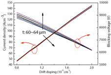
Fig. 1 shows the current density and blocking voltage variation with doping concentration and thickness of epitaxial layer. To achieve a blocking voltage of 6.5 kV, it is determined that the blocking voltage of the epitaxial layer is 8.125 kV, leaving a margin of 25%. The thickness of the epitaxial layer is between 60 to 64 μm, and the blocking voltage per micron is about 120 V. Epitaxial doping concentration is about (1.1−1.3) × 1015 cm−3. Epitaxial wafer thickness and concentration have inter- and intra-chip inhomogeneities. For high-voltage devices, the epitaxial layer contributes most of the resistance and the blocking voltage, so the intra- and inter-wafer uniformity of epitaxial wafer thickness and concentration has a greater impact on the characteristics of the device.
Figure 1.(Color online) Current density and blocking voltage variation with doping concentration and thickness of epitaxial layer.
In this paper, the 6.5 kV SiC MOSFETs were fabricated on a (0001) Si-faced, 4° off-axis toward the < > direction, and N-type 4H-SiC substrate. The nominal voltage was 6.5 kV, and the epitaxial layer ranged from 60 to 65μm thick with an N-type doping concentration of approximately 1.2 × 1015 cm−3. Due to the intra- and inter-wafer uniformity of epitaxial wafer thickness and concentration, the thickness and concentration has a large range. Fig. 2 shows a schematic diagram of the structure of a 6.5 kV SiC MOSFET.
Figure 2.(Color online) Schematic cross-section of 6.5 kV SiC MOSFET.
Al was used as the P-type dopant and N was the N-type dopant. Multiple energy implants of Al and N were implanted to form the P well, P+ body, N+ source and JFET. After all of the ion implantations were made, activation anneal was carried out at 1600–1750 °C for 30 min with carbon cap to maximize lattice recovery and dopant activation. Then, a sacrificial oxidation of 20 nm was conducted to get rid of the surface roughness caused by ion implantation. After that, a 50 nm gate oxide was formed by thermal oxidation followed by NO annealing. Phosphorus-doped polysilicon of 500 nm was then deposited over the gate oxide, followed by gate patterning. 700 nm of inter-layer dielectric was then deposited and patterned to form the ohmic contact window. 150 nm Ni was deposited on the front and backsides of the wafer and rapid thermal annealing (RTP) was carried out at 1000 °C for 2 min to form the ohmic contacts. The interlayer dielectric on the poly-Si was patterned to expose the gate poly-Si pad to form a gate bus. The top metal stack (Ti/Al) was then deposited and patterned to form the source and gate pads. Then, the passivation layer polyimide was deposited and patterned. Lastly, the metal stack (Ti/Ag) was deposition on the backside. The design structure of a floating guard ring edge termination was used for the 6.5 kV conventional planar-gate power MOSFETs. Fig. 3 shows a wafer photo of a 6.5 kV SiC MOSFET. In this article, we use three epitaxial wafers to develop MOSFETs. The parameters of the epitaxial wafers are shown in Table 1. The specific on-resistances contributed by the three types of epitaxial layers are 34.1, 36.5 and 34.8 mΩ·cm2.
In this paper, five kinds of chips with different channel lengths LC and JFET region widths WJ were designed on the wafer. The cell structure parameters are shown in Table 2.
3.1. Influence of epitaxial layer parameters on conduction characteristics
As shown in Fig. 4, the output characteristics of 5 cell structures in 3 epitaxial wafers are compared. The gate–source voltage is 20 V, and the drain-source voltage is 4 V. It can be seen from Fig. 4 that the average current of #1 wafer is the largest, the average current of #3 wafer is second, and the average current of #2 wafer is the smallest. The wafer output current has the same law in the five types of cells. The active area of the five chips is the same, which is 4.7 mm2. Due to the different chip pitches, the edges and corners of the active area of the chip are different, there will be a slight difference in the total cell area but the overall can be ignored. The specific on-resistance of C1 device on the wafer #1 is 44 mΩ·cm2. The resistance of SiC MOSFET consists of substrate resistance, drift region resistance, JFET resistance, accumulation region resistance, channel resistance, source region resistance and ohmic contact resistance. In the case of the same cell structure, the epitaxial layer parameters (i.e., the doping concentration and thickness of the epitaxial wafer) are important factors affecting the conduction characteristics. The greater the thickness w of the epitaxial wafer, the greater the resistance; and the smaller the doping concentration Nd, the higher the resistance. The specific on-resistance contributed by the epitaxial layer is t/(Ndqμ), whereμ is the SiC bulk mobility.
Figure 4.(Color online) Comparison of output current of five chips on three wafers.
The current difference between #1 wafer and #2 wafer is 0.3 A. According to the ID–VDS characteristics of the chip and the chip area, the specific on-resistance difference of #1 wafer and #2 wafer is 0.38 mΩ·cm2 which is similar to epitaxial wafer specific on-resistance difference. For the C4 device, when the JFET width is 3 μm, the proportion of JFET resistance increases, and the effect of epitaxial wafer differences on device conduction is weakened. So the output currents of #2 and #3 are basically the same.
The current distribution uniformity of the #3 wafer is the best, and #2 wafer is the worst, which is largely due to epitaxial layer thickness and doping concentration inhomogeneity. Therefore, the quality of the epitaxial wafer affects the uniformity of the electrical properties of the chip.
3.2. Influence of cell parameters on conduction characteristics
In this paper, the output curves and transfer curves of the devices with five cell parameters are compared at VGS = 20 V, which are shown in Fig. 5. The threshold voltage is determined at the drain-source current of 5 mA by sweeping the gate–source voltage with drain electrodes biased of 10 V. With the increasing channel length, the threshold voltage VGS(th) of the device increases. The on-resistance increases, leading to the drop of the output characteristic curve, and so does the transconductance gfs. With the increasing width of the JFET region, the threshold voltage increases, but the on-resistance decreases. The output characteristic curve moves up, and the three transfer curves cross during the gate voltage increase. When the JFET width is 3 μm, the output curve deviates from the linear region earlier. When Vds is kept constant, the main resistance of the device at low gate voltage comes from channel. The larger the JFET width is, the smaller the cell density and the channel density are. Therefore, at low gate voltage, the device resistance increases with the increase of JFET width. To achieve the same current, such as 5 mA, more gate voltage needs to be applied. Therefore, for the same active area, the wider JFET, the greater the threshold voltage. The change of threshold voltage with channel length is the same as the change of threshold voltage with JFET width.
Figure 5.(Color online) Comparison of output, transfer and derivative parameters of five cell structures. (a) Output characteristic curves. (b) Transfer characteristic curves. (c) Transconductance comparison of different channel lengths. (d) Cell transconductance comparison of different JFET widths.
This article counts the yield of the chips on each wafer. The overall chip area on the wafer is relatively small, so the gate–source yield and blocking yield of the chip are basically the same. We also make a batch of 6.5 kV large-area chips, with the active area of 37 mm2. The gate–source yield and blocking yield are independent of each other[13]. The yield of 6.5 kV MOSFET in this paper is shown in Table 3. The average yields are 40%, 55% and 50%, for the three wafers, respectively. The yield of high-voltage devices decreases rapidly with the increase of defect density and chip area. Reducing the defects in epitaxial materials and those introduced in processes is an important approach to realize commercialization of high-voltage SiC MOSFET devices.
FN tunneling is also called triangular breakdown[14-16]. When the electric field is high enough, the gate oxygen energy level bends to form a triangular shape. When the width of the triangular region is small, electrons directly tunnel. The field strength during FN tunneling is an important parameter for evaluating the quality of the gate oxide. During the preparation of the MOSFET device, the breakdown characteristics of the gate oxide can be tested through the patterned gate oxide capacitor. The I–V curves of gate oxide capacitor are shown in Fig. 6. When Vg is around 35 V, the leakage current of the curve begins to increase rapidly. Therefore, the FN tunneling of this device occurs at an approximate value of 7 MV/cm.
Figure 6.(Color online) Breakdown characteristics of test pattern gate oxide capacitors.
The potential barrier height between the gate oxide and SiC is obtained by transforming the I–V curve[14]. The transforming curves of the gate oxide capacitor I–V curves are shown in Fig. 7.
Figure 7.(Color online) The transforming curves of the gate oxide capacitor I–V curves.
where mox is the mass of electrons in the oxide layer, mox = 0.42m = 3.826 × 10⁻³¹ kg, h is Planck’s constant, h = 6.626 × 10⁻³⁴ J·s.
According to the slopes of the transforming curves, the potential barrier height φb is:
Fig. 8 shows the relationship between barrier height φb and the slope. In our data, the range of slopeB is (1.987−2.125) × 10−8, and the range of φb is 2.75−2.85 eV. It represents a high barrier height between gate oxide and SiC.
Figure 8.(Color online) The relationship between barrier height and slope.
We prepared several 6.5 kV SiC MOSFET modules. Fig. 9 shows 6.5 kV SiC MOSFET package layout and outline. The long-term reliability of the gate oxide were evaluated through high-temperature gate bias tests (HTGB).
Figure 9.(Color online) 6.5 kV SiC MOSFET package layout and outline.
Under two conditions of gate–source bias VGS = –8 V and VGS = 20 V, respectively, the HTGB reliability tests were performed for 650 h at the temperature of 150 °C. Fig. 10 shows the results of high temperature gate bias reliability test for forward gate voltage test and reverse gate voltage test. The gate leakage current is below 5 nA. After the reliability test, there is no degradation of static characteristics for 6.5 kV SiC MOSFET.
Figure 10.High temperature gate bias reliability. (a) Forward gate voltage test results. (b) Reverse gate voltage test results.
3.5. High temperature reverse bias (HTRB) reliability
The high temperature reverse bias reliability is carried out at 150 °C. The gate and source is short-circuited and grounded. The VDS is set to 5.15 kV, and the leakage is tested every two minutes. Fig. 11 shows the leakage results of the HTRB reliability with a total of 560 h. After the HTRB reliability test is completed, the device is retested again. The retest results prove that the device is intact.
Figure 11.The results of high temperature reverse bias reliability.
The structure of the high-voltage 6.5 kV SiC MOSFET device is optimized and developed through process optimization. Based on the electrical characteristics of the device with different epitaxial structures and cell parameters, the following conclusions are drawn:
The specific on-resistance of C1 device on the wafer #1 is 44 mΩ·cm2. The uniformity of the current distribution is large due to inhomogeneity of the epitaxial layer thickness and doping concentration. Therefore, the quality of the epitaxial wafer affects the uniformity of the electrical properties of the chip.
With the decreasing channel length, the threshold voltage VGS(th) of the device decreases and the transconductance increases. As the width of the JFET region increases, the threshold voltage increases and the transconductance first increases and then decreases.
The FN tunneling of the device is about 7 MV/cm, and the barrier height φb ranges from 2.75 to 2.85 eV.
The HTGB tests for 650 h respectively indicate that the gate oxide has good reliability. The 560 h HTRB also passed.
These results show that the design, fabrication and analysis of the device characteristics of 6.5 kV SiC MOSFET will provide important guiding and significant promotion value for its penetration into the power grid field.
Acknowledgements
The authors thank the support of the National Key Research and Development Program (Grant No. 2016YFB0400500) and the Science & Technology Program of the State Grid Corporation of China Co., Ltd. “High voltage and high power SiC materials, devices and the application demonstration in power electronic transformers”.
Lixin Tian, Zechen Du, Rui Liu, Xiping Niu, Wenting Zhang, Yunlai An, Zhanwei Shen, Fei Yang, Xiaoguang Wei. Influence of epitaxial layer structure and cell structure on electrical performance of 6.5 kV SiC MOSFET[J]. Journal of Semiconductors, 2022, 43(8): 082802