• Photonics Research
  • Vol. 10, Issue 7, 1567 (2022)
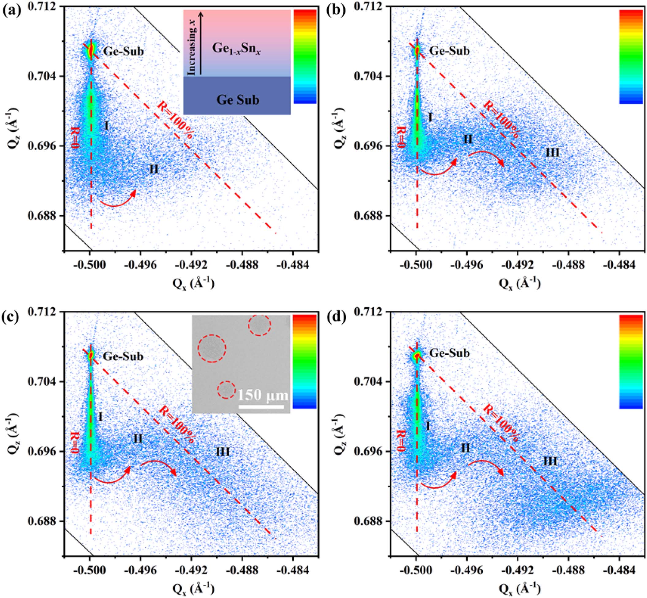
Xiangquan Liu1、2, Jun Zheng1、2、*, Chaoqun Niu1、2, Taoran Liu1、2, Qinxing Huang1、2, Mingming Li1、2, Diandian Zhang1、2, Yaqing Pang1、2, Zhi Liu1、2, Yuhua Zuo1、2, and Buwen Cheng1、2
Author Affiliations
  • 1State Key Laboratory on Integrated Optoelectronics, Institute of Semiconductors, Chinese Academy of Sciences, Beijing 100083, China
  • 2Center of Materials Science and Optoelectronics Engineering, University of Chinese Academy of Sciences, Beijing 100049, China
  • show less
    DOI: 10.1364/PRJ.456000 Cite this Article Set citation alerts
    Xiangquan Liu, Jun Zheng, Chaoqun Niu, Taoran Liu, Qinxing Huang, Mingming Li, Diandian Zhang, Yaqing Pang, Zhi Liu, Yuhua Zuo, Buwen Cheng. Sn content gradient GeSn with strain controlled for high performance GeSn mid-infrared photodetectors[J]. Photonics Research, 2022, 10(7): 1567 Copy Citation Text show less
    RSM around the asymmetric (−2 −2 4) reflection of (a) sample A; (b) sample B; (c) sample C; (d) sample D. The inset of (a) shows an schematic diagram of epitaxial structure of GeSn alloy. The inset of (c) shows an SEM image of sample C, and the positions marked by the red circle are the segregated Sn.
    Fig. 1. RSM around the asymmetric (2  2  4) reflection of (a) sample A; (b) sample B; (c) sample C; (d) sample D. The inset of (a) shows an schematic diagram of epitaxial structure of GeSn alloy. The inset of (c) shows an SEM image of sample C, and the positions marked by the red circle are the segregated Sn.
    Raman scattering spectra of GeSn samples and a Ge wafer for reference, and the position of the ball corresponds to the calculated Ge-Ge Raman shift.
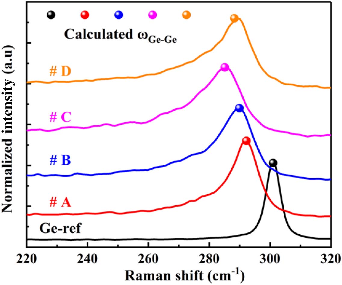
    Fig. 2. Raman scattering spectra of GeSn samples and a Ge wafer for reference, and the position of the ball corresponds to the calculated Ge-Ge Raman shift.
    (a) Full view of XTEM image of sample D; inset: EDX Ge and Sn element mapping. (b) High-resolution XTEM image and FFT pattern of area “b” in (a). (c), (d) Inverse FFT images of the rectangular area in (b).
    Fig. 3. (a) Full view of XTEM image of sample D; inset: EDX Ge and Sn element mapping. (b) High-resolution XTEM image and FFT pattern of area “b” in (a). (c), (d) Inverse FFT images of the rectangular area in (b).
    SIMS profile of Sn composition and bandgap calculations at different depths of (a) sample A; (b) sample B; (c) sample C; (d) sample D. Regions marked with different colors correspond to different strain states of the RSM in Fig. 1.
    Fig. 4. SIMS profile of Sn composition and bandgap calculations at different depths of (a) sample A; (b) sample B; (c) sample C; (d) sample D. Regions marked with different colors correspond to different strain states of the RSM in Fig. 1.
    (a) Three-dimensional schematic of GeSn photodetector with interdigital electrode structure. The inset shows the top view of the device. (b) Working mechanism of GeSn photodetector under light incident conditions. (c) Dark I−V curves of GeSn photodetector at different temperatures. (d) Photocurrent spectra of the GeSn photodetector at 0.2 V for different temperatures.
    Fig. 5. (a) Three-dimensional schematic of GeSn photodetector with interdigital electrode structure. The inset shows the top view of the device. (b) Working mechanism of GeSn photodetector under light incident conditions. (c) Dark IV curves of GeSn photodetector at different temperatures. (d) Photocurrent spectra of the GeSn photodetector at 0.2 V for different temperatures.
    (a) Wavelength-dependent optical responsivity of GeSn photodetector under a bias voltage of 1 V at 77 K. Inset: responsivity at 3 μm as a function of voltage at 77 K. (b) Comparison of cutoff wavelength of GeSn photodetectors in different works.
    Fig. 6. (a) Wavelength-dependent optical responsivity of GeSn photodetector under a bias voltage of 1 V at 77 K. Inset: responsivity at 3 μm as a function of voltage at 77 K. (b) Comparison of cutoff wavelength of GeSn photodetectors in different works.
    SamplesTgrowth (°C)TSn (°C)x (%)RMS (nm)
    A170760–8202.2–8.6 (I)8.6–11.2 (II)1.60
    B150760–8352.0–7.0 (I)7.0–8.9 (II) 8.9–14.2 (III)0.90
    C150760–8502.0–7.3 (I) 7.3–8.7 (II) 8.7–20.3 (III)1.32
    D150760–8352.0–7.1 (I) 7.1–8.7 (II) 8.7–16.3 (III)2.04
    Table 1. Summary of Growth Temperature (Tgrowth), Sn Crucible Temperature (TSn), Measured Sn Content (x), and Root Mean Square (RMS) Roughness of GeSn Samplesa
    ReferenceSn ContentStructureEpitaxial TechniquePeak Specific Detectivity (cmHz1/2W1)Responsivity (A/W)Cutoff Wavelength (μm)
    [16]3%PINMBE0.12 at 1.64 μm at −1 V at RT1.8 μm
    [17]9%QW/PCCVD0.1 at 2.2 μm at 5 V at RT2.4 μm
    [18]10%PCCVD4.6×109 at 77 K1.63 at 1.55 μm at 50 V at 77 K2.4 μm
    [19]10%PINCVD2.4×109 at 77 K0.19 at 1.55 μm at − 0.1 V at RT2.6 μm
    [20]11%PCCVD2.0×1010 at 77 K28.5 at 1.55 μm at 2 V at 77 K3.0 μm
    [21]20%PCCVD1.1×108 at 77 K0.8 at 2.0 μm at 5 V at 77 K3.65 μm
    [22]17%PCCVD0.004 at 2.4 μm at 1  V at RT4.6 μm
    This work16.3%PCMBE9.33×108at 77 K0.35 at 2.53 μm at 1 V at 77 K4.2 μm
    Table 2. Summary of the Performance of GeSn Photodetectorsa
    Xiangquan Liu, Jun Zheng, Chaoqun Niu, Taoran Liu, Qinxing Huang, Mingming Li, Diandian Zhang, Yaqing Pang, Zhi Liu, Yuhua Zuo, Buwen Cheng. Sn content gradient GeSn with strain controlled for high performance GeSn mid-infrared photodetectors[J]. Photonics Research, 2022, 10(7): 1567
    Download Citation