• Journal of Semiconductors
  • Vol. 40, Issue 9, 092001 (2019)
Wenkai Zhu1、2, Xia Wei1、2, Faguang Yan1、2, Quanshan Lv1、2, Ce Hu1、2, and Kaiyou Wang1、2、3、4
Author Affiliations
  • 1State Key Laboratory of Superlattices and Microstructures, Institute of Semiconductors, Chinese Academy of Sciences, Beijing 100083, China
  • 2Center of Materials Science and Optoelectronics Engineering, University of Chinese Academy of Sciences, Beijing 100049, China
  • 3Center for Excellence in Topological Quantum Computation, University of Chinese Academy of Science, Beijing 100049, China
  • 4Beijing Academy of Quantum Information Sciences, Beijing 100193, China
  • show less
    DOI: 10.1088/1674-4926/40/9/092001 Cite this Article
    Wenkai Zhu, Xia Wei, Faguang Yan, Quanshan Lv, Ce Hu, Kaiyou Wang. Broadband polarized photodetector based on p-BP/n-ReS2 heterojunction[J]. Journal of Semiconductors, 2019, 40(9): 092001 Copy Citation Text show less
    (Color online) (a) Structure schematic of BP/ReS2 heterojunction device. The source electrode (the contact connected to ReS2) is grounded. The drain electrode (the contact connected to BP) is applied a voltage Vd. (b) AFM image of p-BP/n-ReS2 heterojunction device. The inset shows the height profile along the red solid line, indicating the thicknesses of BP (~10 nm) and ReS2 (~12 nm). (c) The transfer curve of the ReS2 FET with Au contact was measured at room temperature and Vds = 0.5 V. Top inset: Optical microscope image of the ReS2 FET. The scale bar is 10 μm. The thickness of the ReS2 is about 6 nm. Bottom inset: Current–voltage (Ids–Vds) curves for different gate voltages (Vbg). (d) Ids as a function of Vbg for BP FET at room temperature and Vds = 0.5 V. Top inset: Optical microscope image of the BP FET. The thickness of the BP is about 10 nm. Bottom inset: Ids–Vds curve of the BP FET.
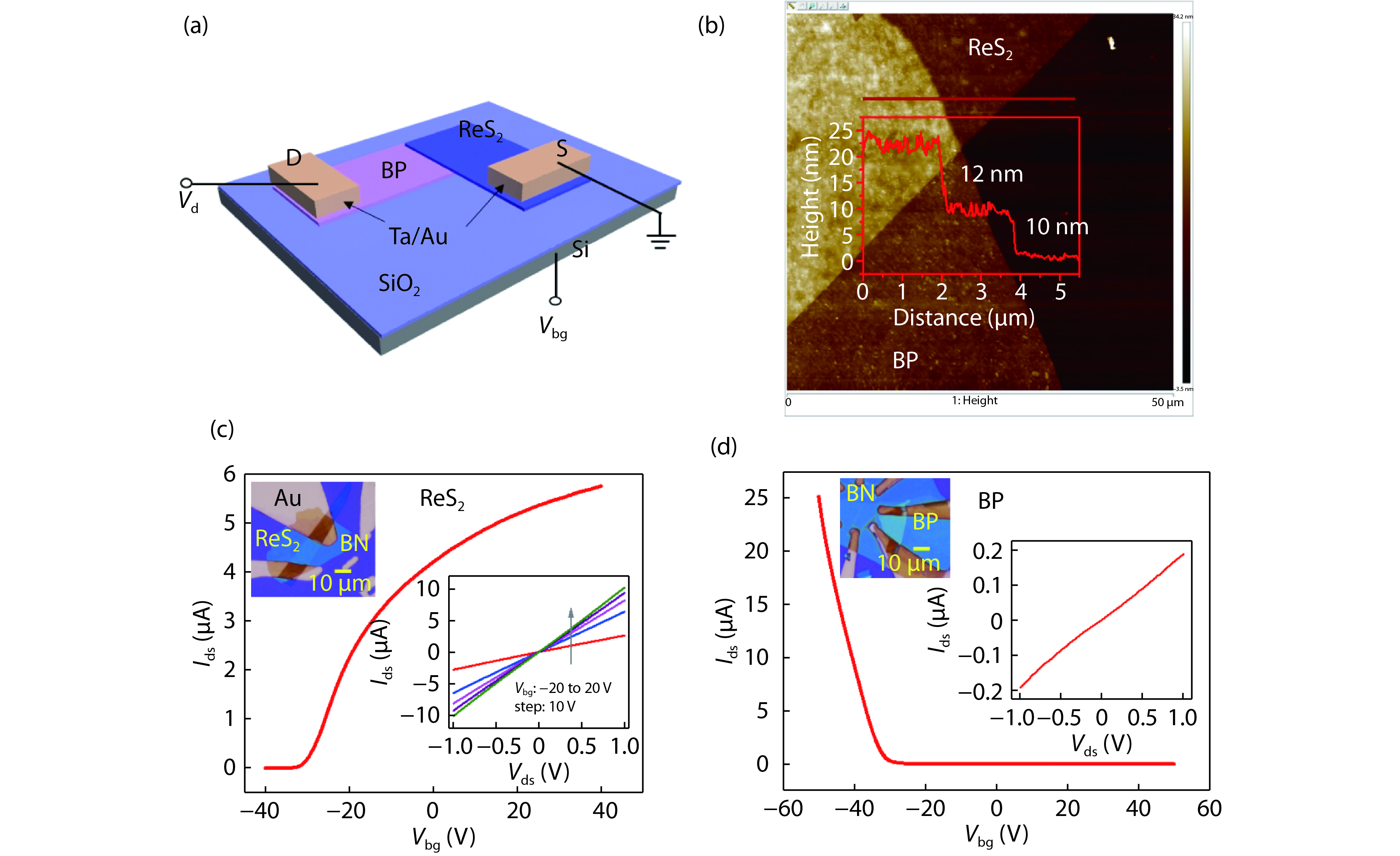
    Fig. 1. (Color online) (a) Structure schematic of BP/ReS2 heterojunction device. The source electrode (the contact connected to ReS2) is grounded. The drain electrode (the contact connected to BP) is applied a voltage Vd. (b) AFM image of p-BP/n-ReS2 heterojunction device. The inset shows the height profile along the red solid line, indicating the thicknesses of BP (~10 nm) and ReS2 (~12 nm). (c) The transfer curve of the ReS2 FET with Au contact was measured at room temperature and Vds = 0.5 V. Top inset: Optical microscope image of the ReS2 FET. The scale bar is 10 μm. The thickness of the ReS2 is about 6 nm. Bottom inset: Current–voltage (IdsVds) curves for different gate voltages (Vbg). (d) Ids as a function of Vbg for BP FET at room temperature and Vds = 0.5 V. Top inset: Optical microscope image of the BP FET. The thickness of the BP is about 10 nm. Bottom inset: IdsVds curve of the BP FET.
    (Color online) (a) Band alignment for isolated p-BP and n-ReS2 layers. Electron affinities of BP and ReS2 are around 4.2 and 4.4 eV, respectively. (b–d) schematic band diagrams at the interface of the BP/ReS2 heterojunction at different applied voltages Vds ((b)zero bias, (c) positive bias and (d) negative bias). The transportation of electrons and holes are indicated by blue arrows and red arrows, respectively.
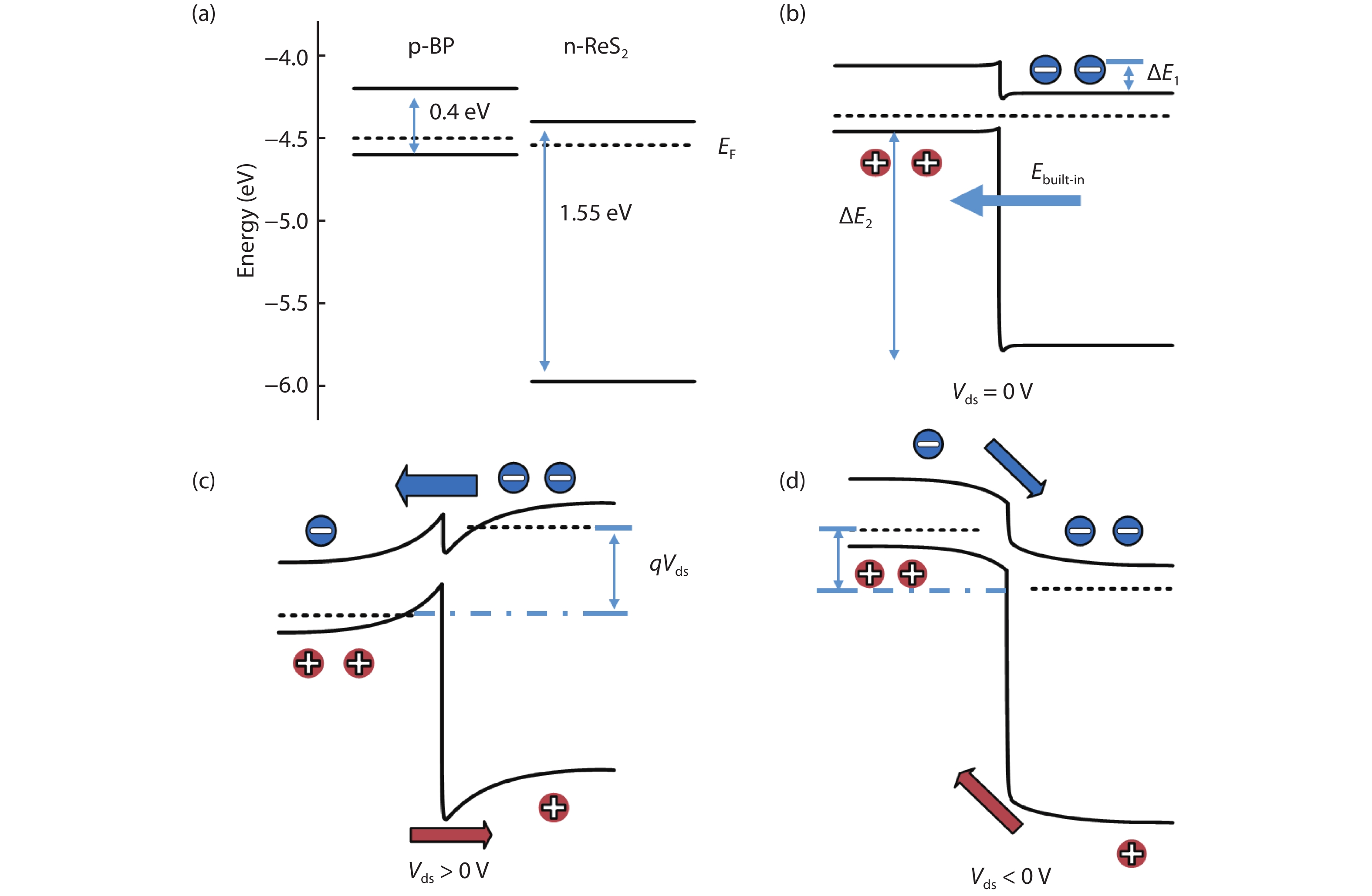
    Fig. 2. (Color online) (a) Band alignment for isolated p-BP and n-ReS2 layers. Electron affinities of BP and ReS2 are around 4.2 and 4.4 eV, respectively. (b–d) schematic band diagrams at the interface of the BP/ReS2 heterojunction at different applied voltages Vds ((b)zero bias, (c) positive bias and (d) negative bias). The transportation of electrons and holes are indicated by blue arrows and red arrows, respectively.
    (Color online) (a) |Ids|–Vds curves of the BP/ReS2 heterojunction device at room temperature in the dark and under illumination with a 1550 nm laser at various excitation intensities (P = 10, 25, 50, 100, 250, 500 W/cm2). (b) Photocurrent as a function of the illumination intensity at different Vds (Vds = 0, –0.4, –1 V). The solid lines are fits to the data. (c) Photoresponsivity (R) of the BP/ReS2 heterojunction device as a function of the illumination intensity at different Vds (Vds = 0, –0.4, –1 V). (d) The external quantum efficiency, EQE, of the heterojunction device as a function of the illumination intensity P at different Vds (Vds = 0, –0.4, –1 V). The wavelength of incident light is 1550 nm.
    Fig. 3. (Color online) (a) |Ids|–Vds curves of the BP/ReS2 heterojunction device at room temperature in the dark and under illumination with a 1550 nm laser at various excitation intensities (P = 10, 25, 50, 100, 250, 500 W/cm2). (b) Photocurrent as a function of the illumination intensity at different Vds (Vds = 0, –0.4, –1 V). The solid lines are fits to the data. (c) Photoresponsivity (R) of the BP/ReS2 heterojunction device as a function of the illumination intensity at different Vds (Vds = 0, –0.4, –1 V). (d) The external quantum efficiency, EQE, of the heterojunction device as a function of the illumination intensity P at different Vds (Vds = 0, –0.4, –1 V). The wavelength of incident light is 1550 nm.
    (Color online) (a) Optical microscope image of the BP/ReS2 heterojunction device, component materials are outlined in different colors. (b) The normalized photocurrent as a function of the illumination wavelength at Vds = –1 V and illumination intensity P = 100 W/cm2. (c), (d) Scanning photocurrent microscope images of the BP/ReS2 heterojunction at Vds = 0 V (c) and –1 V (d) with illumination wavelength 1550 nm (illumination intensity P = 100 W/ cm2). The red dotted line outlines the BP flake and yellow dotted line outlines the ReS2 flake, respectively. The laser beam is focused by microscope objective lens (50×) and the diameter of the spot size is about 5 μm.
    Fig. 4. (Color online) (a) Optical microscope image of the BP/ReS2 heterojunction device, component materials are outlined in different colors. (b) The normalized photocurrent as a function of the illumination wavelength at Vds = –1 V and illumination intensity P = 100 W/cm2. (c), (d) Scanning photocurrent microscope images of the BP/ReS2 heterojunction at Vds = 0 V (c) and –1 V (d) with illumination wavelength 1550 nm (illumination intensity P = 100 W/ cm2). The red dotted line outlines the BP flake and yellow dotted line outlines the ReS2 flake, respectively. The laser beam is focused by microscope objective lens (50×) and the diameter of the spot size is about 5 μm.
    (Color online) (a) Time dependences of Ids during incident light switched on/off at Vds = –1 V with different wavelength (λ = 400, 532, 1064, 1320, 1550 nm). (b) Source–drain current Ids as a function of time with photoswitching at different Vds (Vds = 0, –0.2, –0.4, –0.6, –0.8, –1 V). The light intensity P = 50 W/cm2.
    Fig. 5. (Color online) (a) Time dependences of Ids during incident light switched on/off at Vds = –1 V with different wavelength (λ = 400, 532, 1064, 1320, 1550 nm). (b) Source–drain current Ids as a function of time with photoswitching at different Vds (Vds = 0, –0.2, –0.4, –0.6, –0.8, –1 V). The light intensity P = 50 W/cm2.
    (Color online) (a) Optical microscope image of the BP/ReS2 heterojunction device. The angles of zero degree and 90 degree represents the rotation direction of the linearly polarized light. (b), (c) The anisotropic response in Iph plotted in the polar coordination at visible light wavelength of 532 and 650 nm. The visible light intensity P = 25 W cm2. (d–f) The evolution of the Iph plotted in the polar coordination at near infrared light wavelength of (d) 1064 nm, (e) 1550 nm, and (f) 1750 nm. The near infrared light intensity P = 100 W/ cm2. The Vds is fixed in –1 V.
    Fig. 6. (Color online) (a) Optical microscope image of the BP/ReS2 heterojunction device. The angles of zero degree and 90 degree represents the rotation direction of the linearly polarized light. (b), (c) The anisotropic response in Iph plotted in the polar coordination at visible light wavelength of 532 and 650 nm. The visible light intensity P = 25 W cm2. (d–f) The evolution of the Iph plotted in the polar coordination at near infrared light wavelength of (d) 1064 nm, (e) 1550 nm, and (f) 1750 nm. The near infrared light intensity P = 100 W/ cm2. The Vds is fixed in –1 V.
    Wenkai Zhu, Xia Wei, Faguang Yan, Quanshan Lv, Ce Hu, Kaiyou Wang. Broadband polarized photodetector based on p-BP/n-ReS2 heterojunction[J]. Journal of Semiconductors, 2019, 40(9): 092001
    Download Citation