
Wenkai Zhu, Xia Wei, Faguang Yan, Quanshan Lv, Ce Hu, Kaiyou Wang. Broadband polarized photodetector based on p-BP/n-ReS2 heterojunction[J]. Journal of Semiconductors, 2019, 40(9): 092001
- Journal of Semiconductors
- Vol. 40, Issue 9, 092001 (2019)
Abstract
1. Introduction
Two dimensional (2D) van der Waals (vdWs) crystals, such as graphene[
Black phosphorus is a layered material, where each phosphorus atom is bonded covalently to three neighboring atoms forming a puckered orthorhombic lattice. The BP is a direct bandgap semiconductor. The band gap of BP is dependent on the number of layers, which increases from ~0.3 eV for bulk to ~2 eV for monolayer limit[
Rhenium disulphide (ReS2) as a member of TMDCs also have been extensively investigated[
Recently, the reported BP-on-WSe2 heterostructure photodetector exhibits a broadband photoresponsivity in a spectral range of 400–1550 nm[
2. Experiments
Fabrication of the BP/ReS2 heterojunction-based polarized photodetector devices. First, a BP (from HQ graphene) flake was exfoliated onto polydimethylsiloxane (PDMS) stamps by adhesive tape. The stamps are adhered to a glass slide. Under optical microscope, the BP flake with appropriate thickness and shape can be chosen. Afterwards, the target BP flake was transferred onto a 300 nm thick SiO2/Si substrate by using a site-controllable dry transfer method[
Electrical and optoelectrical properties were measured using a semiconductor characterization system (Agilent Technology B1500A) and a lock-in amplifier (SR830) with a light chopper. The visible to NIR light illumination was provided by a Fianium WhiteLase supercontinuum laser source. The output light was tuned into monochromatic light by an Omni-λ300 monochromator. For the spatially-dependent photocurrent measurement, a microscope objective lens (50×), a lock-in amplifier (SR830) with a light chopper and a micromechanical stage were combined. Linearly polarized light was obtained by making a laser beam pass through a Glan-Taylor prism (polarizer) and a half-wave plate (HWP). The polarization direction of the light was controlled by rotating the HWP while keeping the incident laser power a constant.
Calculation details of the FET device mobility: The field-effect mobility can be calculated using the equation μ = (L/W)(d/ε0εrVds)(∆Ids/∆Vbg), where L and W are the length and width of the channel respectively, d is the oxide thickness, ε0 and εr are the permittivity of free space and the relative permittivity of the SiO2, and the last term is the slope of the transfer curve in the linear regime of the ON state.
3. Results and discussion
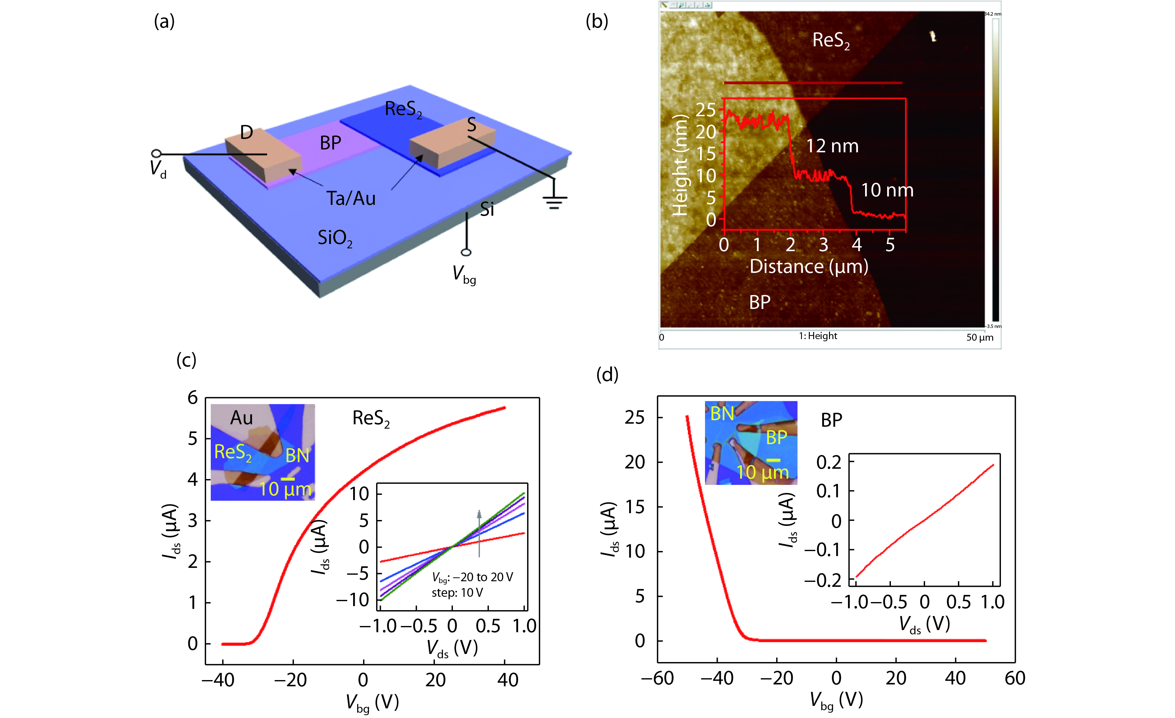
Characteristic of the BP/ReS2 heterojunction device. Fig. 1(a) presents a schematic of our heterojunction device. All of the devices were prepared by mechanical exfoliation and site-controllable dry transfer method. The detailed fabrication processes has been provided in the experimental section. An AFM image of the p-BP/n-ReS2 heterojunction is shown in Fig. 1(b), with the height profile along the red solid line being shown in the inset, indicating the thicknesses of BP (~10 nm) and ReS2 (~12 nm). We first performed the electrical characterizations of the ReS2 FET and BP FET at room temperature. Fig. 1(c) shows the transfer curve of the ReS2 FET with a linear plot of the source-drain current (Ids) versus back gate voltage (Vbg) at a fixed source–drain voltage (Vds = 0.5 V). The device shows an n-type FET behaviors with electron mobility of ~29 cm2V–1s–1 (see the experimental section for the calculation details), which is consistent with the reported value[
![]()
Figure 1.(Color online) (a) Structure schematic of BP/ReS2 heterojunction device. The source electrode (the contact connected to ReS2) is grounded. The drain electrode (the contact connected to BP) is applied a voltage
In addition to the conductive type of the materials, the energy band structure of the materials is also very important for construction of a p–n junction. The energy band diagrams of the heterojunction in the isolated and different bias states are illustrated in Figs. 2(a)–2(d). Based on previous reports, the electron affinity and bandgap (Eg) of multilayer BP are around 4.2 and 0.4 eV, respectively[
![]()
Figure 2.(Color online) (a) Band alignment for isolated p-BP and n-ReS2 layers. Electron affinities of BP and ReS2 are around 4.2 and 4.4 eV, respectively. (b–d) schematic band diagrams at the interface of the BP/ReS2 heterojunction at different applied voltages
To investigate the responsivity of the device dependence on the illumination intensities, different illumination intensities P ranging from 0 to 500 W/cm2 are applied to the heterojunction device. Fig. 3(a) shows the |Ids|–Vds curves of the BP/ReS2 heterojunction device at room temperature in the dark and under illumination with a 1550 nm laser at various excitation intensities (P = 10, 25, 50, 100, 250, 500 W/cm2). The |Ids|–Vds curve of the device in the dark exhibits a clear rectifying behavior. The rectification ratio, defined as the ratio of the forward/reverse current, is about 50 at Vds = +1/–1 V. This behavior can be attributed to the formation of p–n diode within the atomically thin BP/ReS2 heterojunction (more details see band alignment of the BP/ReS2 heterojunction). The device exhibits a low dark current (~1.0 nA) at Vds = –1 V. Under a light illumination, electron-hole pairs are generated and separated by the electric field in the heterojunction, which generate the photocurrents. Photocurrent (Iph) is defined as the difference between drain currents with and without light-illumination (Iph = |Ilight – Idark|). Under reverse bias (Vds < 0 V), Iph increases with increasing the light intensity P. Iph can also be enhanced by increasing the reverse bias (shown in Fig. 3(b)). It can be explained by the increased electrical field in the heterojunction under reverse bias (Fig. 2(d)). The increased electrical field decreases the carrier transit time, thus reduces the recombination probability of the photo-generated electrons and holes. In addition, Iph exhibits a sublinear dependence on the incident light intensity P and follows a power law of Iph ∝ Pα, where α = 0.61, 0.68, and 0.73 at Vds = 0, –0.4 and –1 V, respectively. Larger value α can be obtained by applied a larger reverse bias, which also benefits from the shorter carrier transit time. The similar sublinear behavior has also been reported for other similar structures, such as ReS2 FETs[
![]()
Figure 3.(Color online) (a) |
The image of the BP/ReS2 heterojunction device shown in Fig. 4(a), where the boundaries of each layer are indicated by dotted lines with different colors. The corresponding scale bar is 10 µm. Fig. 4(b) shows the normalized photocurrent as a function of the illumination wavelength at Vds = –1 V and illumination intensity P = 100 W/cm2, which demonstrates the BP/ReS2 heterojunction device exhibits obvious photoresponse over a broad spectral range (400–1800 nm), from the visible to near infrared. The maximum normalized Iph ~ 1 is obtained at wavelength of 550 nm, and the minimum normalized Iph ~ 0.013 is obtained at wavelength of 1025 nm. Therefore, the device can be used for broadband photodetection. ReS2 has the strongest absorption in the ultraviolet and visible band, but weaker absorption in the near infrared bands[
![]()
Figure 4.(Color online) (a) Optical microscope image of the BP/ReS2 heterojunction device, component materials are outlined in different colors. (b) The normalized photocurrent as a function of the illumination wavelength at
The excellent stability is an important condition for the application of photodetectors. For investigate the stability of the device, the device was illuminated by a laser with different wavelength (or under different Vds) and light intensity P = 50 W/cm2. Fig. 5(a) presents the time dependences of |Ids| during incident light switched on/off at Vds = –1 V with different wavelength (λ = 400, 532, 1064, 1320, 1550 nm), which shows the device can steady working over a broad spectral range, from visible to near infrared. In addition, the photoswitch ratio (Ilight/Idark) of the device is about 23 at 400 nm, 25 at 532 nm, 12 at 1064, 13 at 1320, and 7 at 1550 nm. Source–drain current |Ids| as a function of time with photoswitching at different Vds (Vds = 0, –0.2, –0.4, –0.6, –0.8, –1 V) shown in the Fig. 5(b). A stabilized photoresponsivity ~ 0.4 mA/W was achieved at λ = 1550 nm under zero bias, which shows the device can work as a self-driven near infrared photodetectors. Moreover, after many cycles, the photocurrent still responds in a similar fashion to the light, which exhibits excellent operation reversibility and stability.
![]()
Figure 5.(Color online) (a) Time dependences of
To examine the polarization sensitivity of the device, the device was illuminated by linearly polarized light with different polarized angle. The photocurrent as a function of polarized angle under different illumination wavelength is shown in Fig. 6. The optical microscope image of the BP/ReS2 heterojunction device is exhibited in Fig. 6(a). The angles of zero degree and 90 degree represents the rotation direction of the linearly polarized light. The anisotropic response in |Iph| plotted in the polar coordination at visible light wavelength of 532 nm (Fig. 6(b)) and 650 nm (Fig. 6(c)). The visible light intensity P = 25 W/cm2. Figs. 6(d)–6(f) presents the evolution of the |Iph| plotted in the polar coordination at near infrared light wavelength of 1064 nm (Fig. 6(d)), 1550 nm (Fig. 6(e)), and 1750 nm (Fig. 6(f)). The near infrared light intensity P = 100 W/cm2. The results show the device can act as a polarized photodetector over a broad spectral range (from 532 to 1750 nm). The double symmetry has been observed. The direction of the maximum photocurrent is perpendicular to the direction of the minimum photocurrent. The polarization sensitive absorption of the BP/ReS2 heterojunction photodetector is induced by crystal structure anisotropy. Because of the intrinsic low carrier mobility and high electron–hole recombination rate in ReS2[
![]()
Figure 6.(Color online) (a) Optical microscope image of the BP/ReS2 heterojunction device. The angles of zero degree and 90 degree represents the rotation direction of the linearly polarized light. (b), (c) The anisotropic response in
4. Conclusion
In conclusion, we have fabricated BP/ReS2 vdWs heterojunction devices by dry-transfer of 2D flakes method. The devices realize broadband photoresponse from visible to near infrared (NIR) (400–1800 nm) with stable and repeatable photoswitch characteristics, and the photoresponsivities reached 1.8 mA/W at 1550 nm. In addition, the polarization sensitive detection form the visible to NIR spectrum (532–1750 nm) was demonstrated, which shows a highly polarization sensitive photocurrent with an anisotropy ratio as high as 2.98 at 532 nm, 3.39 at 650 nm, 6.44 at 1064 nm, 5.5 at 1550 nm, and 4.3 at 1750 nm. Because of the intrinsic low carrier mobility and high electron–hole recombination rate in ReS2, the polarization sensitivity of ReS2 is relatively low. Thus, the polarization sensitive absorption of the BP/ReS2 heterojunction device is mainly induced by crystal structure anisotropy of BP. Our study shows that van der Waals heterojunction is an effective way to realize the broadband polarization sensitive photodetection, which is of great significance to the application of multi-functional devices based on 2D vdWs heterostructures.
Acknowledgements
This work was supported by the National Key R&D Program of China (Grant No. 2017YFA0303400 and No.2017YFB0405700). This work was also supported by the NSFC Grant Nos. 61774144 and 11474272. The project was sponsored by Chinese Academy of Sciences, grant No. QYZDY-SSW-JSC020, XDPB12, and XDB28000000.
References
[1] K S Novoselov, A K Geim, S V Morozov et al. Electric field effect in atomically thin carbon films. Science, 306, 666(2004).
[2] L Li, Y Yu, G J Ye et al. Black phosphorus field-effect transistors. Nat Nanotechnol, 9, 372(2014).
[3] P Vogt, P De Padova, C Quaresima et al. Silicene: compelling experimental evidence for graphenelike two-dimensional silicon. Phys Rev Lett, 108, 155501(2012).
[4] L C Gomes, A Carvalho. Phosphorene analogues: Isoelectronic two-dimensional group-IV monochalcogenides with orthorhombic structure. Phys Rev B, 92, 085406(2015).
[5] A Splendiani, L Sun, Y Zhang et al. Emerging photoluminescence in monolayer MoS2. Nano Lett, 10, 1271(2010).
[6] Q H Wang, K Kalantar-Zadeh, A Kis et al. Electronics and optoelectronics of two-dimensional transition metal dichalcogenides. Nat Nanotechnol, 7, 699(2012).
[7] Y Cao, K Cai, P Hu et al. Strong enhancement of photoresponsivity with shrinking the electrodes spacing in few layer GaSe photodetectors. Sci Rep, 5, 8130(2015).
[8] W Luo, Y Cao, P Hu et al. Gate tuning of high-performance InSe-based photodetectors using graphene electrodes. Adv Opt Mater, 3, 1418(2015).
[9] J R Schaibley, H Yu, G Clark et al. Valleytronics in 2D materials. Nat Rev Mater, 1, 16055(2016).
[10] D Akinwande, N Petrone, J Hone. Two-dimensional flexible nanoelectronics. Nat Commun, 5, 5678(2014).
[11] Q Feng, F Yan, W Luo et al. Charge trap memory based on few-layer black phosphorus. Nanoscale, 8, 2686(2016).
[12] C N R Rao, K Gopalakrishnan, U Maitra. Comparative study of potential applications of graphene, MoS2, and other two-dimensional materials in energy devices, sensors, and related areas. ACS Appl Mater Interfaces, 7, 7809(2015).
[13] F Pizzocchero, L Gammelgaard, B S Jessen et al. The hot pick-up technique for batch assembly of van der Waals heterostructures. Nat Commun, 7, 11894(2016).
[14] G Konstantatos, E H Sargent. Nanostructured materials for photon detection. Nat Nanotechnol, 5, 391(2010).
[15] C Gong, Y Zhang, W Chen et al. Electronic and optoelectronic applications based on 2D novel anisotropic transition metal dichalcogenides. Adv Sci, 4, 1700231(2017).
[16] J S Tyo, D L Goldstein, D B Chenault et al. Review of passive imaging polarimetry for remote sensing applications. Appl Opt, 45, 5453(2006).
[17] F Yan, Z Wei, X Wei et al. Toward high-performance photodetectors based on 2D materials: strategy on methods. Small Methods, 2, 1700349(2018).
[18] X Wei, F G Yan, C Shen et al. Photodetectors based on junctions of two-dimensional transition metal dichalcogenides. Chin Phys B, 26, 038504(2017).
[19] L Ye, P Wang, W Luo et al. Highly polarization sensitive infrared photodetector based on black phosphorus-on-WSe2 photogate vertical heterostructure. Nano Energy, 37, 53(2017).
[20] V Tran, R Soklaski, Y Liang et al. Layer-controlled band gap and anisotropic excitons in few-layer black phosphorus. Phys Rev B, 89, 235319(2014).
[21] Z Zhou, Y Cui, P H Tan et al. Optical and electrical properties of two-dimensional anisotropic materials. J Semicond, 40, 061001(2019).
[22] J Qiao, X Kong, Z X Hu et al. High-mobility transport anisotropy and linear dichroism in few-layer black phosphorus. Nat Commun, 5, 4475(2014).
[23] H Yuan, X Liu, F Afshinmanesh et al. Polarization-sensitive broadband photodetector using a black phosphorus vertical p–n junction. Nat Nanotechnol, 10, 707(2015).
[24] E Zhang, Y Jin, X Yuan et al. ReS2-based field-effect transistors and photodetectors. Adv Funct Mater, 25, 4076(2015).
[25] M Rahman, K Davey, S Z Qiao. Advent of 2D rhenium disulfide (ReS2): fundamentals to applications. Adv Funct Mater, 27, 1606129(2017).
[26] S Tongay, H Sahin, C Ko et al. Monolayer behaviour in bulk ReS2 due to electronic and vibrational decoupling. Nat Commun, 5, 3252(2014).
[27] N R Pradhan, A McCreary, D Rhodes et al. Metal to insulator quantum-phase transition in few-layered ReS2. Nano Lett, 15, 8377(2015).
[28] Y C Lin, H P Komsa, C H Yeh et al. Single-layer ReS2: two-dimensional semiconductor with tunable in-plane anisotropy. ACS Nano, 9, 11249(2015).
[29] F Liu, S Zheng, X He et al. Highly sensitive detection of polarized light using anisotropic 2D ReS2. Adv Funct Mater, 26, 1169(2016).
[30] E Liu, M Long, J Zeng et al. High responsivity phototransistors based on few-layer ReS2 for weak signal detection. Adv Funct Mater, 26, 1938(2016).
[31] S Cao, Y Xing, J Han et al. Ultrahigh-photoresponsive UV photodetector based on a BP/ReS2 heterostructure p–n diode. Nanoscale, 10, 16805(2018).
[32] X K Li, X G Gao, B W Su et al. Polarization-dependent photocurrent of black phosphorus/rhenium disulfide heterojunctions. Adv Mater Interfaces, 5, 1800960(2018).
[33] A Castellanos-Gomez, M Buscema, R Molenaar et al. Deterministic transfer of two-dimensional materials by all-dry viscoelastic stamping. 2D Mater, 1, 011002(2014).
[34] D J Perello, S H Chae, S Song et al. High-performance n-type black phosphorus transistors with type control via thickness and contact-metal engineering. Nat Commun, 6, 7809(2015).
[35] J Shim, S Oh, D H Kang et al. Phosphorene/rhenium disulfide heterojunction-based negative differential resistance device for multi-valued logic. Nat Commun, 7, 13413(2016).
[36] S H Jo, H W Lee, J Shim et al. Highly efficient infrared photodetection in a gate-controllable Van der Waals heterojunction with staggered bandgap alignment. Adv Sci, 5, 1700423(2018).
[37] M Massicotte, P Schmidt, F Vialla et al. Picosecond photoresponse in van der Waals heterostructures. Nat Nanotechnol, 11, 42(2015).
[38] Y Xue, Y Zhang, Y Liu et al. Scalable production of a few-layer MoS2/WS2 vertical heterojunction array and its application for photodetectors. ACS Nano, 10, 573(2016).
[39] Q Lv, F Yan, X Wei et al. High-performance, self-driven photodetector based on graphene sandwiched GaSe/WS2 heterojunction. Adv Opt Mater, 6, 1700490(2018).
[40] F Yan, L Zhao, A Patane et al. Fast, multicolor photodetection with graphene-contacted p-GaSe/n-InSe van der Waals heterostructures. Nanotechnology, 28, 27L(2017).
[41] X Wei, F Yan, Q Lv et al. Fast gate-tunable photodetection in the graphene sandwiched WSe2/GaSe heterojunctions. Nanoscale, 9, 8388(2017).
[42] X Wei, F Yan, Q Lv et al. Enhanced photoresponse in MoTe2 photodetectors with asymmetric graphene contacts. Adv Opt Mater, 0, 1900190(2019).
[43] W Wu, Q Zhang, X Zhou et al. Self-powered photovoltaic photodetector established on lateral monolayer MoS2-WS2 heterostructures. Nano Energy, 51, 45(2018).
[44] H Liu, B Xu, J M Liu et al. Highly efficient and ultrastable visible-light photocatalytic water splitting over ReS2. Phys Chem Chem Phys, 18, 14222(2016).
[45] S Huang, X Ling. Black phosphorus: optical characterization, properties and applications. Small, 13, 1700823(2017).
[46] X Ling, S Huang, E H Hasdeo et al. Anisotropic electron-photon and electron-phonon interactions in black phosphorus. Nano Lett, 16, 2260(2016).
[47] X Wang, Y Li, L Huang et al. Short-wave near-infrared linear dichroism of two-dimensional germanium selenide. J Am Chem Soc, 139, 14976(2017).


Set citation alerts for the article
Please enter your email address

© Copyright 2018-2021 | Chinese Laser Press. All Rights Reserved 沪ICP备15018463号-20