• Advanced Photonics
  • Vol. 4, Issue 6, 066002 (2022)
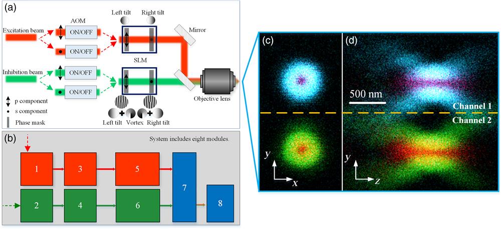
Dazhao Zhu1、†, Liang Xu2, Chenliang Ding1, Zhenyao Yang1, Yiwei Qiu1, Chun Cao1, Hongyang He3, Jiawei Chen3, Mengbo Tang1, Lanxin Zhan1, Xiaoyi Zhang1, Qiuyuan Sun1, Chengpeng Ma1, Zhen Wei1, Wenjie Liu1、2, Xiang Fu4, Cuifang Kuang1、2、*, Haifeng Li1、2, and Xu Liu1、2、*
Author Affiliations
  • 1Zhejiang Lab, Research Center for Intelligent Chips and Devices, Hangzhou, China
  • 2Zhejiang University, College of Optical Science and Engineering, State Key Laboratory of Modern Optical Instrumentation, Hangzhou, China
  • 3Zhejiang University, College of Control Science and Engineering, State Key Laboratory of Industrial Control Technology, Hangzhou, China
  • 4Zhejiang Lab, Research Center for Humanoid Sensing, Zhejiang Lab, Hangzhou, China
  • show less
    DOI: 10.1117/1.AP.4.6.066002 Cite this Article Set citation alerts
    Dazhao Zhu, Liang Xu, Chenliang Ding, Zhenyao Yang, Yiwei Qiu, Chun Cao, Hongyang He, Jiawei Chen, Mengbo Tang, Lanxin Zhan, Xiaoyi Zhang, Qiuyuan Sun, Chengpeng Ma, Zhen Wei, Wenjie Liu, Xiang Fu, Cuifang Kuang, Haifeng Li, Xu Liu. Direct laser writing breaking diffraction barrier based on two-focus parallel peripheral-photoinhibition lithography[J]. Advanced Photonics, 2022, 4(6): 066002 Copy Citation Text show less
    Proposed P3L system and focal spots: (a) schematic of the P3L system and (b) physical arrangement with eight modules. (c), (d) Focal spots located near the x−y and y−z planes, respectively. The light blue and green spots were generated by the 532-nm beam, and the purple and red spots were produced by the 780-nm beam, forming two combinations. The combination of light blue and purple spots was named channel 1, and the other combination was named channel 2. (c) and (d) share the same scale bar.
    Fig. 1. Proposed P3L system and focal spots: (a) schematic of the P3L system and (b) physical arrangement with eight modules. (c), (d) Focal spots located near the xy and yz planes, respectively. The light blue and green spots were generated by the 532-nm beam, and the purple and red spots were produced by the 780-nm beam, forming two combinations. The combination of light blue and purple spots was named channel 1, and the other combination was named channel 2. (c) and (d) share the same scale bar.
    Two-dimensional feature size verification experiment results. (a) Feature size versus inhibition beam intensity under excitation beam exposure with different powers. (b) SEM image of the nanowire obtained at the point in the red box in (a). After the PPI is turned on, the line width is compressed from 138.8 to 39.8 nm. Scale bar: 100 nm.
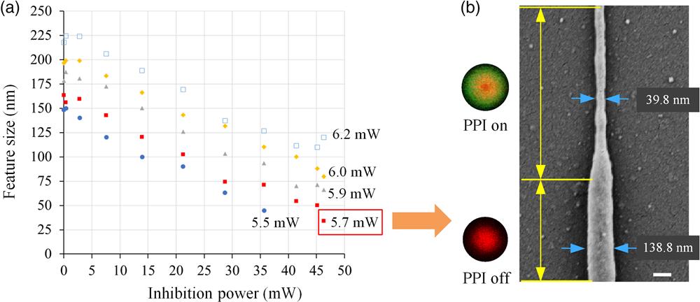
    Fig. 2. Two-dimensional feature size verification experiment results. (a) Feature size versus inhibition beam intensity under excitation beam exposure with different powers. (b) SEM image of the nanowire obtained at the point in the red box in (a). After the PPI is turned on, the line width is compressed from 138.8 to 39.8 nm. Scale bar: 100 nm.
    Bit-pattern-printing results. (a) Full-view SEM image of the printed pattern. The pattern shows two lines of text and is pixelated. Top line: Chinese words, printed by channel 1 with PPI; bottom line: English words (translation of the text in the top line), printed by channel 2 without PPI. Scale bar: 2 μm. (b), (c) Enlarged views of the yellow and blue boxes in (a), respectively; the horizontal and vertical pitches of the bits are 200 nm. Scale bars: 1 μm.
    Fig. 3. Bit-pattern-printing results. (a) Full-view SEM image of the printed pattern. The pattern shows two lines of text and is pixelated. Top line: Chinese words, printed by channel 1 with PPI; bottom line: English words (translation of the text in the top line), printed by channel 2 without PPI. Scale bar: 2  μm. (b), (c) Enlarged views of the yellow and blue boxes in (a), respectively; the horizontal and vertical pitches of the bits are 200 nm. Scale bars: 1  μm.
    Metamaterial cubic-unit printing results: (a) SEM image of a 2×2×2 unit cell, (b) top view of (a), (c) zoomed-in view of the yellow box in (a), (d) SEM image of a 3×3×3 unit cell, (e) top view of (d), and (f) zoomed-in view of the yellow box in (d). In (b) and (c), the portions corresponding to the light-blue stripes were printed by channel 1, and those indicated by the dark-red stripes were printed by channel 2. Scale bars: 50 μm.
    Fig. 4. Metamaterial cubic-unit printing results: (a) SEM image of a 2×2×2 unit cell, (b) top view of (a), (c) zoomed-in view of the yellow box in (a), (d) SEM image of a 3×3×3 unit cell, (e) top view of (d), and (f) zoomed-in view of the yellow box in (d). In (b) and (c), the portions corresponding to the light-blue stripes were printed by channel 1, and those indicated by the dark-red stripes were printed by channel 2. Scale bars: 50  μm.
    Oblique-view SEM images of 3D nanostructures parallel-printed using two spots. (a) Two cubical box frames, (b) periodic structure: hexagonal fence, (c) wire structure: nanophotonic wires, and (d) spherical structure: buckyball model. Scale bars: 10 μm.
    Fig. 5. Oblique-view SEM images of 3D nanostructures parallel-printed using two spots. (a) Two cubical box frames, (b) periodic structure: hexagonal fence, (c) wire structure: nanophotonic wires, and (d) spherical structure: buckyball model. Scale bars: 10  μm.
    Dazhao Zhu, Liang Xu, Chenliang Ding, Zhenyao Yang, Yiwei Qiu, Chun Cao, Hongyang He, Jiawei Chen, Mengbo Tang, Lanxin Zhan, Xiaoyi Zhang, Qiuyuan Sun, Chengpeng Ma, Zhen Wei, Wenjie Liu, Xiang Fu, Cuifang Kuang, Haifeng Li, Xu Liu. Direct laser writing breaking diffraction barrier based on two-focus parallel peripheral-photoinhibition lithography[J]. Advanced Photonics, 2022, 4(6): 066002
    Download Citation