Abstract
Direct laser writing (DLW) enables arbitrary three-dimensional nanofabrication. However, the diffraction limit poses a major obstacle for realizing nanometer-scale features. Furthermore, it is challenging to improve the fabrication efficiency using the currently prevalent single-focal-spot systems, which cannot perform high-throughput lithography. To overcome these challenges, a parallel peripheral-photoinhibition lithography system with a sub-40-nm two-dimensional feature size and a sub-20-nm suspended line width was developed in our study, based on two-photon polymerization DLW. The lithography efficiency of the developed system is twice that of conventional systems for both uniform and complex structures. The proposed system facilitates the realization of portable DLW with a higher resolution and throughput.
Author Presentation Playback
1 Introduction
Peripheral photoinhibition (PPI) direct laser writing (DLW) is a lithography technology used to improve the feature size in two-photon polymerization (2PP) DLW.1–4 In the concept and implementation, it is analogous to stimulated-emission depletion microscopy,5–7 which uses two beams with opposite functions: a Gaussian-shaped induction beam causing fluorescence excitation and a doughnut-shaped inhibition beam quenching it at the periphery.8 Subdiffraction PPI-DLW relies on the precise spatiotemporal overlapping of these two beams.9 In the peripheral region, photoexcitation of the Gaussian-shaped beam is inhibited and polymerization is prevented; therefore, only the central excited region is polymerized.10–13 In this way, nanofeature sizes breaking the diffraction barrier can be achieved.
Previous scholars have reported minimum lateral feature sizes below 100 nm.1,11,14 Cao et al.15 achieved a 40-nm feature size and a 130-nm resolution with excitation and inhibition beam wavelengths of 488 and 375 nm, respectively. Gan et al.8 achieved a single line with a 9-nm feature size and two adjacent lines with a 52-nm resolution using excitation and inhibition beam wavelengths of 800 and 375 nm, respectively. He et al.16 applied a twin-oval-shaped beam instead of a doughnut-shaped beam in PPI-DLW with excitation and inhibition beam wavelengths of 800 and 532 nm, respectively, and stably obtained a 45-nm single nanowire.
DLW is remarkably advantageous, due to its maskless and vacuum-free operation, three-dimensional (3D) lithography capability,17 and cost-effectiveness.18–20 Therefore, it has been used to fabricate many functional nanostructures that are employed in photonics,21–23 electronics,24–27 and life sciences.28–30 In addition to the aforementioned advantages, PPI-DLW offers a subdiffraction feature size, making it a powerful tool for the fields mentioned above.28–30
Sign up for Advanced Photonics TOC. Get the latest issue of Advanced Photonics delivered right to you!Sign up now
However, the throughput of single-beam/spot DLW is a noticeable disadvantage that greatly restricts the applicability of PPI-DLW.31 This problem can be addressed by performing parallel lithography with multifocal arrays, especially when fabricating periodic structures.32–35 Since 2005, several research groups have aimed at such multipoint parallel processing. Multispot generation methods include the use of microlens arrays, beam-splitting devices, spatial light modulators (SLMs), and deformable-mirror devices (DMDs). Microlens arrays and beam-splitting devices are less flexible than SLMs and DMDs.
Among these devices, SLMs36–41 are the most commonly used. Wegener et al.42 implemented a system using diffraction elements to achieve nine points and printed a metamaterial structure containing 108,000 3D units. In PPI-DLW, both Gaussian- and doughnut-shaped multifocal beams can be generated via phase modulation with an SLM.33 Before printing, many phase maps are needed; they can be acquired via phase-retrieving arithmetic based on the pattern or structure to be printed. The phase maps uploaded on the SLM control the light field (specifically the beam on–off). As the beam is scanned, the phase map loaded on the SLM is continuously switched. Thus the individual and dynamic on–off control of a single spot in an array is restricted by the SLM frame rate. Moreover, if the pattern or structure is quite complex and nonperiodic, the iterative Fourier transform required for the phase map is time- and hard-drive-memory-consuming.43,44 Consequently, the overall efficiency of multifocal-based printing is restricted. Therefore, more efficient on–off control methods would be highly desirable to improve the printing speed of multifocal systems.
To overcome these challenges and restrictions, this paper reports a parallel peripheral-photoinhibition lithography () system that attains a subdiffraction feature size and improves the lithography efficiency, outperforming the currently prevalent single-focal-spot systems. To double the efficiency, the proposed system employs two printing channels, each of which is formed by an excitation solid spot and an inhibition doughnut spot to realize PPI. The individual control of each channel enables them to print different patterns simultaneously, resulting in a system that is more functional than one with a uniform focus control. The position and separation of the spots can also be easily controlled, making the system flexible. The proposed system can achieve a sub-40-nm two-dimensional (2D) feature size and a sub-20-nm suspended line width. The remainder of this paper is organized as follows. Section 2 describes the proposed system, with further details in the Supplementary Material. In Sec. 3, many experiment results including feature size verification and 3D structure parallel printing are presented. A discussion and outlook are provided in Sec. 4. Finally, this work is concluded in Sec. 5.
2 Materials and Methods
2.1 Proposed System
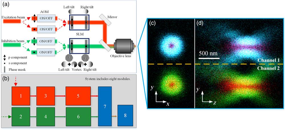
For the excitation and inhibition beams, the polarization property of light is used to generate two focal spots by utilizing an SLM, corresponding to the s- and p-polarized components of the beam. Individual and dynamic on–off and aberration control can be realized for both the excitation and inhibition spots. Figure 1(a) provides a schematic of the proposed system, and Fig. 1(b) depicts its physical arrangement. The system includes eight modules numbered 1–8, as shown in Fig. 1(b). First, the s- and p-polarized components of the beam are split so that they can be individually controlled; then they are modulated by the left and right tilt phase masks (loaded on the SLM) so that the s- and p-components generate two separate spots after focusing. The distances between the spots and their positions can be adjusted using the tilt coefficient. For the inhibition beam, a vortex phase (loaded on the SLM) is utilized to generate a doughnut spot. The wavelength of the excitation beam is 780 nm (Coherent, Chameleon Vision II, 3 W, Glasgow, UK; pulsed 80-MHz repetition rate), and that of the inhibition beam is 532 nm (Laser Quantum, Opus 532-5W, Stockport, UK; continuous wave). Modules 1 and 2, 3 and 4, and 5 and 6 are the same; they differ only in having different optical elements fit for different wavelengths. Modules 1 and 2 (MRC, Heidelberg, Germany) are used for beam-pointing stabilization. Modules 3 and 4 first split the excitation/inhibition beam into two beams using a polarizing beam splitter (PBS), so that the individual on–off control of each beam can be realized using an acoustic-optical modulator (AOM). Then the two beams are recombined using another PBS. Modules 5 and 6 perform phase modulation using SLMs. The polarization property of SLMs is completely leveraged; the s- and p-components are modulated by different areas on the SLM screen, and a quarter-wave plate is used for the polarization shift.45,46 In module 7, the excitation and inhibition beams are combined and then successively passed through a galvanometer scanner (CTI, 8310K, Lexington, Massachusetts) and a scan lens (Nikon, PROJ-XSD007835 A1, Tokyo, Japan). In module 8, a microscope with an objective lens (Nikon, NA 1.45, , Tokyo, Japan) is used for beam focusing and photoresist-sample holding. Additional details regarding each module and the entire system are provided in Figs. S1–S5 in the Supplementary Material.

Figure 1.Proposed system and focal spots: (a) schematic of the system and (b) physical arrangement with eight modules. (c), (d) Focal spots located near the and planes, respectively. The light blue and green spots were generated by the 532-nm beam, and the purple and red spots were produced by the 780-nm beam, forming two combinations. The combination of light blue and purple spots was named channel 1, and the other combination was named channel 2. (c) and (d) share the same scale bar.
The scanning imaging function was utilized to verify the quality of the spots (two excitation solid spots and two inhibition doughnut spots) by imaging 150-nm-diameter gold beads, as shown in Figs. 1(c) and 1(d), in which one excitation solid spot and one inhibition doughnut spot are superposed in three dimensions. The vortex phase was used to modulate the inhibition light. The primary wavefront aberrations were corrected carefully by applying Zernike polynomials.47,48 To present the features of our system concisely, a pattern containing two lines of the test is shown in Fig. S6 in the Supplementary Material. The final phase masks loaded on the SLMs are depicted in Figs. S7(a) and S7(b) in the Supplementary Material. The distances and relative positions of the two spots were quantitatively controlled by adjusting the tip and tilt coefficient through careful calibration. The system was also used to generate a traditional 3D dark spot (Fig. S8 in the Supplementary Material).
2.2 PSF Verification and Image Acquisition
The galvanometer, AOM, piezostage, and trigger signals to the PMT were controlled by external voltages. An eight-channel analog-out card (National Instruments, NI PXIe-6733, Austin, Texas) provided these voltage signals, and another DAQ card (National Instruments, NI PXIe-6363, Austin, Texas) was used for data acquisition. The two cards were synchronized via a PXIe chassis (National Instruments, NI PXIe-1073, Austin, Texas), which was controlled through a manufacturer-supplied dynamic link library and C++ software developed in-house. Scanning could be conducted in any region of interest in the , , and planes, and images could be automatically acquired once the parameters were set.
2.3 Printing Manner and Monitoring
Except for the cubic metamaterial sample, which was printed in a dip-in manner, all the samples in this study were printed in the conventional oil–substrate–photoresist manner: the objective lens on the inverted microscope was immersed in oil and the photoresist was presented on the substrate. We used a glass slide as a substrate (refractive index: 1.51) and fixed it on the piezostage using a specially designed adaptor holder. The widefield image was acquired by a charge-coupled device camera, and the software was provided by the manufacturer. Four instant snapshots taken during the parallel printing process for the two lines of text are shown in Fig. S7(c) in the Supplementary Material (Video 1, MP4, 6.995 MB [URL: https://doi.org/10.1117/1.AP.4.6.066002.s1]). The substrate was illuminated from above by a light-emitting diode light source (wavelength, 625 nm, Thorlabs, CHROLITS-C1, Newton, New Jersey; driver, Thorlabs, LEDD1B, Newton, New Jersey). All the laser powers were measured at the aperture before the objective lens on the microscope by a power meter (power sensor, S121C, Thorlabs; power and energy meter console, Thorlabs, Newton, New Jersey).
2.4 Materials and Sample Processing
A formulation containing 0.5 g of 7-diethylamino-3-thenoylcoumarin, 8.6 g of tricyclodecane dimethanol diacrylate, 0.7 g of ethoxylated bisphenyl fluorene diacrylate, and 0.7 g of o-phenyl phenoxyethyl acrylate was used as the sample photoresist.49 The exposed samples were developed in propylene glycol 1-monomethyl ether 2-acetate for 15 min, followed by rinsing in isopropanol for 5 min. A 2-nm-thick gold layer was evaporated on the samples prior to topography observation.
3 Results
3.1 2D Sub-40-nm Feature Size Verification
We printed a nanowire on a glass substrate (-thick microscope coverslip) with and without PPI to verify the feature size of our system. Many previous works have shown that, for a certain focal-spot speed, the final feature size is sensitive to both the excitation and inhibition powers. The spot speed was set to , and five excitation powers were chosen for each inhibition power, as shown in Fig. 2(a). Figure 2(b) shows a scanning electron microscopy (SEM) image of the nanowire at the excitation and inhibition powers indicated by the red box in Fig. 2(a), demonstrating that the line width is reduced from 138.8 to 39.8 nm. Suspended nanowires were also printed for further demonstration, and the experimental results are presented in Figs. S9 and S10 in the Supplementary Material.
Figure 2.Two-dimensional feature size verification experiment results. (a) Feature size versus inhibition beam intensity under excitation beam exposure with different powers. (b) SEM image of the nanowire obtained at the point in the red box in (a). After the PPI is turned on, the line width is compressed from 138.8 to 39.8 nm. Scale bar: 100 nm.
3.2 Bit Dot Pattern Printing
Because large data-recording systems are important potential applications of multifocal DLW, we printed a bit pattern to verify the feasibility of our system. The pattern in Fig. 2 was pixelated and reprinted using PPI-2PP and 2PP. The pitch of the bits was set to 200 nm. The dwell time of one dot was , the excitation spot power was 14.5 mW, and the inhibition power was 41.0 mW. The results are presented in Fig. 3: the bit dots printed with PPI [upper line in Fig. 3(a)] are clearly resolved with distinct gaps; by contrast, the bit dots printed without PPI [lower line in Fig. 3(a)] are blurred. The two lines of text were still printed simultaneously, whereas the two lines must be printed individually in a normal single-beam-path system. Consequently, the efficiency of our method is twice that of a normal single-beam-path system. Further experimental verification can be found in Fig. S11(a) in the Supplementary Material, which depicts two different bit dot patterns printed by two channels with PPI. In addition, two square-wave patterns with a 150-nm bit gap were printed, and the results are presented in Figs. S11(b) and S11(c) in the Supplementary Material.
Figure 3.Bit-pattern-printing results. (a) Full-view SEM image of the printed pattern. The pattern shows two lines of text and is pixelated. Top line: Chinese words, printed by channel 1 with PPI; bottom line: English words (translation of the text in the top line), printed by channel 2 without PPI. Scale bar: . (b), (c) Enlarged views of the yellow and blue boxes in (a), respectively; the horizontal and vertical pitches of the bits are 200 nm. Scale bars: .
3.3 Three-Dimensional Structure Printing
To test the parallel printing of an actual 3D nanostructure, a metamaterial architecture50 (a cube) was printed. This cube was used as a bench sample in Ref. 42. Here we considered two cells as bench samples: one containing units and the other containing units. The unit 3D models and more relative results are shown in Fig. S12 in the Supplementary Material. Because of the individual control of the light beam, the distance between the two focal spots did not need to match the size of the unit to make one spot print one unit, which makes the system more flexible. In fact, we could also have generated more spots in the focal plane to print the units simultaneously using the SLM, but that was out of the scope of this experiment. For this micron-scale structure, a sub-100-nm feature size was not required; therefore, the cells were printed without PPI. The distance between the two spots was adjusted to , and the power of a single spot was 31.5 mW. The objective lens was changed to (Nikon, NA 1.45, Japan), and the focal-spot speed was [step size: ]. The corresponding results are presented in Fig. 4, where the size of each cell is . Three-fold stitching was required, and the areas printed by different spots are marked by different colors in Figs. 4(b) and 4(c).
Figure 4.Metamaterial cubic-unit printing results: (a) SEM image of a unit cell, (b) top view of (a), (c) zoomed-in view of the yellow box in (a), (d) SEM image of a unit cell, (e) top view of (d), and (f) zoomed-in view of the yellow box in (d). In (b) and (c), the portions corresponding to the light-blue stripes were printed by channel 1, and those indicated by the dark-red stripes were printed by channel 2. Scale bars: .
To demonstrate the feasibility of the 3D fabrication method further, additional 3D structures were printed. First, two cubic frames were printed by the two spots simultaneously. The two frames were of the same size but had different patterns (squares and circles), as shown in Fig. 5(a). Each spot printed one frame, the separation of the two spots was , and the side length was . Second, three types of continuous 3D nanostructures were printed: periodic, wire, and spherical structures, and oblique-view SEM images of these structures are provided in Figs. 5(b)–5(d), respectively. Figure 5(b) shows a periodic fence array with 10 hexagonal cells; each cell has a side length of and a height of . The photonic wire is a functional nanostructure used to connect integrated circuits across chip boundaries. We printed a photonic-wire structure model containing four wires crossing each other spatially [Fig. 5(c)]. A -diameter buckyball model was also printed [Fig. 5(d)]. For these structures, the objective lens was changed back to . The focal-spot power was 15.2 mW, and the speed was set to [step size: ]. A few 2.5D structures were also printed as additional evidence, and the results can be found in Fig. S13 in the Supplementary Material.
Figure 5.Oblique-view SEM images of 3D nanostructures parallel-printed using two spots. (a) Two cubical box frames, (b) periodic structure: hexagonal fence, (c) wire structure: nanophotonic wires, and (d) spherical structure: buckyball model. Scale bars: .
4 Discussion and Outlook
Multifocus parallel scanning and the PPI technique can enable potential breakthroughs in DLW optical fabrication. Herein, we proposed a two-focus parallel scanning strategy with minimal hardware updates for system stability. Furthermore, the identical on–off control of each focus verifies the possibility of rapid parallel lithography of nonperiodic patterns and structures, increasing the flexibility of DLW. The proposed method enables rapid and identical on–off control of each focus with a modulation frequency on the order of a megahertz, which can also be achieved using an SLM. However, the SLM frequency is the maximum possible on–off frequency, and the typical frame rate of the SLM is only 60 Hz (the highest is 1 kHz, which is still considerably lower than the AOM frequency). If the pattern to be printed is significantly complex and nonperiodic, resulting in a beam on–off frequency on the order of a megahertz, a system that uses an SLM to generate multiple foci is unsuitable. One solution to this problem is to decrease the scanning speed to lower the on–off frequency. Notably, it is difficult to realize parallel printing of complex and nonperiodic patterns by employing an SLM alone without compromising the scanning speed. Our method addresses this problem using an AOM to modulate every subbeam. It can, therefore, enable the parallel printing of nonperiodic and complex patterns without compromising the scanning speed. Moreover, because our system uses SLMs, it can still generate multiple foci to print identical patterns or use a relatively low on–off beam frequency to print nonidentical ones.
For a DLW system, reducing the time cost required to fabricate large-scale structures or patterns is a major challenge. Parallel scanning is a feasible solution to this problem. However, another important issue is related to the stitching process, particularly for systems using galvanometer scanners. In the proposed system, the separation distance between the two spots can be controlled by adjusting the tilt parameter following the Zernike polynomials. However, it is impossible to increase the distance without any limits. Therefore, when printing certain large structures or patterns, a stitching process is required, which introduces artifact-related issues. The mechanism that causes artifacts in the stitching process is complicated. The factors affecting this mechanism include the properties of the photoresist; mechanical properties of the structure to be printed; printing parameters; and uniformity in the shape, power, and focus depth of the two spots. In galvanometer-based multifocal-spot systems, stitching-induced artifacts constitute a considerable problem that should be addressed in the future research.
The proposed system can provide a sub-50-nm feature size in direct-writing lithography and extend the potential application range of DLW optical fabrication. In particular, for the fabrication of certain 3D structures with dimensions of several hundred nanometers, traditional 2PP-DLW with a feature size of more than 100 nm may encounter sampling and subdivision issues owing to the relatively large pixel volumes, which may lead to increased roughness of the fabricated structures. Electron beam lithography provides smaller feature sizes; however, its ability to fabricate special 3D structures is quite limited. By using PPI, the proposed system enables the DLW optical fabrication of various fine 3D structures, such as those of nanoscale optical elements including blazed gratings, microlens arrays, microfluidic structures, and metasurfaces. Therefore, the proposed system can serve as a useful tool for supporting the development of numerous fields.
5 Conclusion
Our proposed system improves the throughput of DLW by fully utilizing the polarized components of the light. The printing efficiency achieved with a double-beam path is twice that of traditional DLW. Moreover, the two channels in the system can execute different printing tasks, enabling it to fabricate not only periodic structures but also highly complex ones. Further, a sub-40-nm 2D feature size and a sub-20-nm suspended line width were achieved using the PPI mechanism. The parallel PPI-DLW method can improve the throughput of optical nanofabrication. However, despite the improved efficiency, a large performance gap remains between this approach and projection lithography. Additional multifocal-system strategies should be explored in future work, especially ones involving rapid independent control of focal spots.
Biographies of the authors are not available.
References
[1] R. Wollhofen et al. 120 nm resolution and 55 nm structure size in STED-lithography. Opt. Express, 21, 10831-10840(2013).
[2] T. A. Klar, R. Wollhofen, J. Jacak. Sub-Abbe resolution: from STED microscopy to STED lithography. Phys. Scr., T162, 014049(2014).
[3] S. W. Hell. Microscopy and its focal switch. Nat. Methods, 6, 24-32(2009).
[4] M. Elmeranta et al. Characterization of nanostructures fabricated with two-beam DLW lithography using STED microscopy. Opt. Mater. Express, 6, 3169-3179(2016).
[5] S. W. Hell, J. Wichmann. Breaking the diffraction resolution limit by stimulated emission: stimulated-emission-depletion fluorescence microscopy. Opt. Lett., 19, 780-782(1994).
[6] T. A. Klar et al. Fluorescence microscopy with diffraction resolution barrier broken by stimulated emission. Proc. Natl. Acad. Sci. U. S. A., 97, 8206-8210(2000).
[7] K. I. Willig et al. STED microscopy reveals that synaptotagmin remains clustered after synaptic vesicle exocytosis. Nature, 440, 935-939(2006).
[8] Z. Gan et al. Three-dimensional deep sub-diffraction optical beam lithography with 9 nm feature size. Nat. Commun., 4, 2061(2013).
[9] J. Fischer et al. Exploring the mechanisms in STED-enhanced direct laser writing. Adv. Opt. Mater., 3, 221-232(2015).
[10] T. F. Scott et al. Two-color single-photon photoinitiation and photoinhibition for subdiffraction photolithography. Science, 324, 913-917(2009).
[11] J. Fischer, G. von Freymann, M. Wegener. The materials challenge in diffraction-unlimited direct-laser-writing optical lithography. Adv. Mater., 22, 3578-3582(2010).
[12] J. T. Fourkas. Nanoscale photolithography with visible light. J. Phys. Chem. Lett., 1, 1221-1227(2010).
[13] J. Fischer, M. Wegener. Ultrafast polymerization inhibition by stimulated emission depletion for three-dimensional nanolithography. Adv. Mater., 24, OP65-OP69(2012).
[14] R. Wollhofen et al. Functional photoresists for sub-diffraction stimulated emission depletion lithography. Opt. Mater. Express, 7, 2538-2559(2017).
[15] Y. Cao et al. High-photosensitive resin for super-resolution direct-laser-writing based on photoinhibited polymerization. Opt. Express, 19, 19486-19494(2011).
[16] X. He et al. STED direct laser writing of 45 nm width nanowire. Micromachines, 10, 726(2019).
[17] J. Fischer, M. Wegener. Three-dimensional optical laser lithography beyond the diffraction limit. Laser Photonics Rev., 7, 22-44(2013).
[18] K. Sugioka et al. Femtosecond laser 3D micromachining: a powerful tool for the fabrication of microfluidic, optofluidic, and electrofluidic devices based on glass. Lab Chip, 14, 3447-3458(2014).
[19] K. Sugioka, Y. Cheng. Femtosecond laser three-dimensional micro- and nanofabrication. Appl. Phys. Rev., 1, 041303(2014).
[20] L. Q. Tao et al. A flexible 360-degree thermal sound source based on laser induced graphene. Nanomaterials, 6, 112(2016).
[21] C. Kachris, I. Tomkos. A survey on optical interconnects for data centers. IEEE Commun. Surv. Tutorials, 14, 1021-1036(2012).
[22] R. R. Gattass, E. Mazur. Femtosecond laser micromachining in transparent materials. Nat. Photonics, 2, 219-225(2008).
[23] H. Zeng et al. High-resolution 3D direct laser writing for liquid-crystalline elastomer microstructures. Adv. Mater., 26, 2319-2322(2014).
[24] B. Buchegger et al. Stimulated emission depletion lithography with mercapto-functional polymers. ACS Nano, 10, 1954-1959(2016).
[25] M. Deubel et al. Direct laser writing of three-dimensional photonic-crystal templates for telecommunications. Nat. Mater., 3, 444-447(2004).
[26] W. Gao et al. Direct laser writing of micro-supercapacitors on hydrated graphite oxide films. Nat. Nanotechnol., 6, 496-500(2011).
[27] Z.-L. Wu et al. Polymer-based device fabrication and applications using direct laser writing technology. Polymers, 11, 553(2019).
[28] P. Mueller et al. Molecular switch for sub-diffraction laser lithography by photoenol intermediate-state cis–trans isomerization. ACS Nano, 11, 6396-6403(2017).
[29] M. Wiesbauer et al. Nano-anchors with single protein capacity produced with STED lithography. Nano Lett., 13, 5672-5678(2013).
[30] C. Wolfesberger et al. Streptavidin functionalized polymer nanodots fabricated by visible light lithography. J. Nanobiotechnol., 13, 27(2015).
[31] S. K. Saha et al. Scalable submicrometer additive manufacturing. Science, 366, 105-109(2019).
[32] K. Kataoka et al. Laser printer optics with use of slant scanning of multiple beams. Appl. Opt., 36, 6294-6307(1997).
[33] X. Li et al. Multifocal optical nanoscopy for big data recording at 30 TB capacity and gigabits/second data rate. Optica, 2, 567-570(2015).
[34] J. Jin et al. Multi-channel vortex beam generation by simultaneous amplitude and phase modulation with two-dimensional metamaterial. Adv. Mater. Technol., 2, 1600201(2017).
[35] F. Formanek et al. Three-dimensional fabrication of metallic nanostructures over large areas by two-photon polymerization. Opt. Express, 14, 800-809(2006).
[36] J. I. Kato et al. Multiple-spot parallel processing for laser micronanofabrication. Appl. Phys. Lett., 86, 044102(2005).
[37] X. Z. Dong, Z. S. Zhao, X. M. Duan. Micronanofabrication of assembled three-dimensional microstructures by designable multiple beams multiphoton processing. Appl. Phys. Lett., 91, 124103(2007).
[38] S. D. Gittard et al. Fabrication of microscale medical devices by two-photon polymerization with multiple foci via a spatial light modulator. Biomed. Opt. Express, 2, 3167-3178(2011).
[39] W. Yan, B. P. Cumming, M. Gu. High-throughput fabrication of micrometer-sized compound parabolic mirror arrays by using parallel laser direct-write processing. J. Opt., 17, 075803(2015).
[40] L. Yang et al. Parallel direct laser writing of micro-optical and photonic structures using spatial light modulator. Opt. Lasers Eng., 70, 26-32(2015).
[41] Q. Geng et al. Ultrafast multi-focus 3-D nano-fabrication based on two-photon polymerization. Nat. Commun., 10, 2179(2019).
[42] V. Hahn et al. Rapid assembly of small materials building blocks (voxels) into large functional 3D metamaterials. Adv. Funct. Mater., 30, 1907795(2020).
[43] J. Miao, D. Sayre, H. N. Chapman. Phase retrieval from the magnitude of the Fourier transforms of nonperiodic objects. J. Opt. Soc. Am. A, 15, 1662-1669(1998).
[44] S. G. Podorov, K. M. Pavlov, D. M. Paganin. A non-iterative reconstruction method for direct and unambiguous coherent diffractive imaging. Opt. Express, 15, 9954-9962(2007).
[45] M. O. Lenz et al. 3-D stimulated emission depletion microscopy with programmable aberration correction. J. Biophotonics, 7, 29-36(2014).
[46] D. Zhu et al. Compact three-dimensional super-resolution system based on fluorescence emission difference microscopy. Opt. Commun., 405, 157-163(2017).
[47] T. J. Gould et al. Adaptive optics enables 3D STED microscopy in aberrating specimens. Opt. Express, 20, 20998-21009(2012).
[48] S. Deng et al. Investigation of the influence of the aberration induced by a plane interface on STED microscopy. Opt. Express, 17, 1714-1725(2009).
[49] C. Cao et al. Dip-in photoresist for photoinhibited two-photon lithography to realize high-precision direct laser writing on wafer. ACS Appl. Mater. Interfaces, 14, 31332-31342(2022).
[50] T. Frenzel, M. Kadic, M. Wegener. Three-dimensional mechanical metamaterials with a twist. Science, 358, 1072-1074(2017).