Yuan Liu, Youqiang Huang, Yingjie Zhao, Gongxun Bai, Shiqing Xu. Luminescence Properties of Doped Two-Dimensional Materials[J]. Laser & Optoelectronics Progress, 2021, 58(15): 1516014
Search by keywords or author
- Laser & Optoelectronics Progress
- Vol. 58, Issue 15, 1516014 (2021)
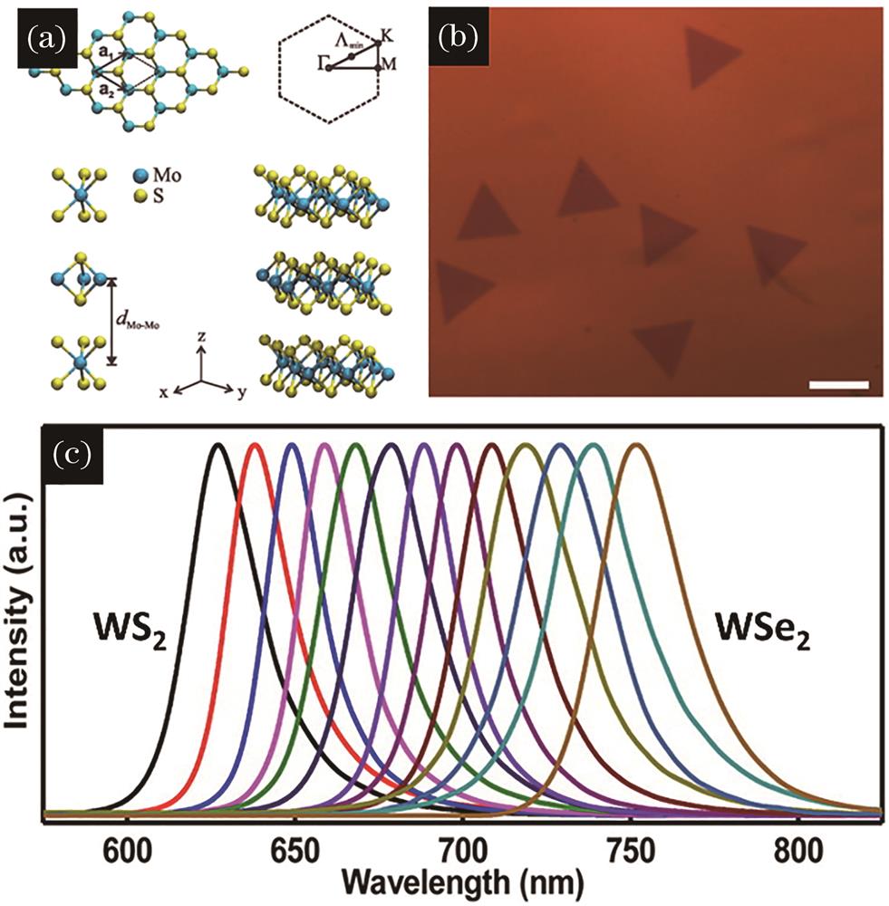
![The crystal structure, optical images,and photoluminescence (PL) of two-dimensional transition-metal dichalcogenide. (a) The diagram of the crystal structure of MoS2[35];(b) the optical images of WSxSe2-x monolayer[36]; (c) the normalized PL spectra of WSxSe2-x monolayer with different ratios[36]](/richHtml/lop/2021/58/15/1516014/img_1.jpg)
Fig. 1. The crystal structure, optical images,and photoluminescence (PL) of two-dimensional transition-metal dichalcogenide. (a) The diagram of the crystal structure of MoS2[35];(b) the optical images of WSxSe2-x monolayer[36]; (c) the normalized PL spectra of WSxSe2-x monolayer with different ratios[36]
![PL spectra in 2D black phosphorus (BP). (a) PL spectra of BP nanosheets with different layer numbers[44]; (b) the relationship between the emitting photon energy and layer number[45]; (c) the excitation polarization angle dependence of PL intensity[49]; (d) both emission and excitation energies dependence of PL intensity mapping[49]](/richHtml/lop/2021/58/15/1516014/img_2.jpg)
Fig. 2. PL spectra in 2D black phosphorus (BP). (a) PL spectra of BP nanosheets with different layer numbers[44]; (b) the relationship between the emitting photon energy and layer number[45]; (c) the excitation polarization angle dependence of PL intensity[49]; (d) both emission and excitation energies dependence of PL intensity mapping[49]
Fig. 3. Elements for the composition of the 2D materials and luminescent doped ions in periodic table
Fig. 4. Transition electron microscope (TEM) images and PL spectra of the transition-metal doped 2D materials. (a) The HR-TEM image of the Mn doped MoS2[57]; (b) the HAADF-STEM image of the Nb-doped WS2[58]; (c) the PL spectra of the Mn-doped MoS2 monolayer on sapphire, the Mn-doped MoS2 monolayer on the silica wafer,and the pristine MoS2 monolayer[57]; (d) the PL spectra of the doped and undoped WS2[58]
Fig. 5. The microstructure and PL property of the Er doped MoS2 monolayer[59]. (a) The CS-STEM image of the atomic scale MoS2∶Er; (b) the anti-Stokes emission of the MoS2∶Er monolayer; (c) the Stokes emission of the MoS2∶Er monolayer; (d) the anti-Stokes emission of the different position on the area (200 μm × 100 μm)
Fig. 6. The microstructure and PL properties of the Nd doped 2D In2Se3 nanosheets[60]. (a) The TEM image of the Nd doped 2D In2Se3 nanosheets; (b) the intrinsic PL spectra of the Nd doped bulk In2Se3 and In2Se3 nanosheets; (c) the Stokes emission of the Nd doped 2D In2Se3 nanosheets; (d) the luminescence decay curve of the 1057 nm in as-prepared nanosheets
Fig. 7. The microstructure, Raman spectra, and the PL spectra of the Er doped 2D ZnSe nanosheets[61]. (a) The TEM image of the ZnSe∶Er nanosheets; (b) Raman spectra of the ZnSe∶Er nanosheets; (c) the Stokes emission of the ZnSe∶Er nanosheets at 4 K; (d) the anti-Stokes emission of the ZnSe∶Er nanosheets at 4 K
Fig. 8. The microstructure and PL and EL spectra of the Yb, Er codoped 2D nanosheets,and the diagram of the LED[62]. (a) The optical image of the Yb, Er codoped 2D nanosheets; (b) the anti-Stokes emission of the Yb, Er codoped 2D nanosheets under 980 nm excitation; (c) the EL spectrum of the tungsten selenide and molybdenum selenide heterojunction; (d) the diagram of the LED based on Yb, Er codoped tungsten selenide and molybdenum selenide heterojunction

Set citation alerts for the article
Please enter your email address


