
Xiaotong Fan, Tingzhu Wu, Bin Liu, Rong Zhang, Hao-Chung Kuo, Zhong Chen. Recent developments of quantum dot based micro-LED based on non-radiative energy transfer mechanism[J]. Opto-Electronic Advances, 2021, 4(4): 210022-1
- Opto-Electronic Advances
- Vol. 4, Issue 4, 210022-1 (2021)
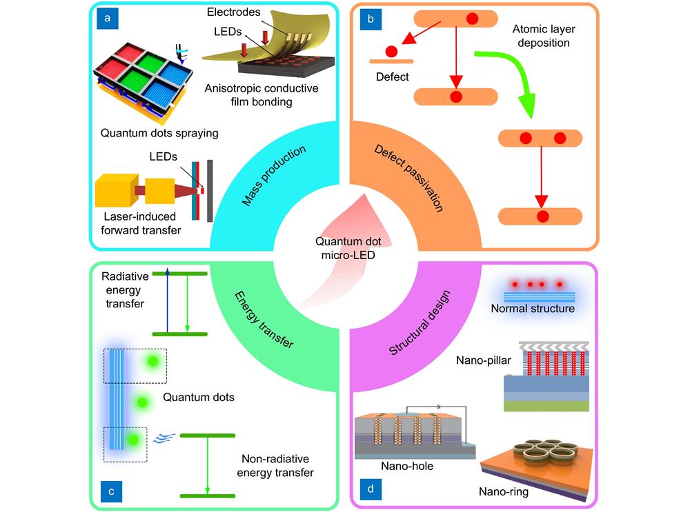
Fig. 1. The corresponding developments of QD micro-LED. (a ) The methods of mass production. (b ) Atomic layer deposition passivation. (c ) The mechanism of energy transfer between micro-LED chip and QDs. (d ) Structural design for QD micro-LEDs. Figures reproduced with permission from: (a) ref.14, Royal Society of Chemistry; ref.15, under a Creative Commons Attribution License; ref.22, Chinese Laser Press; (d) ref.28, Optical Society of America; ref.29, John Wiley and Sons; ref.30, under a Creative Commons Attribution License.
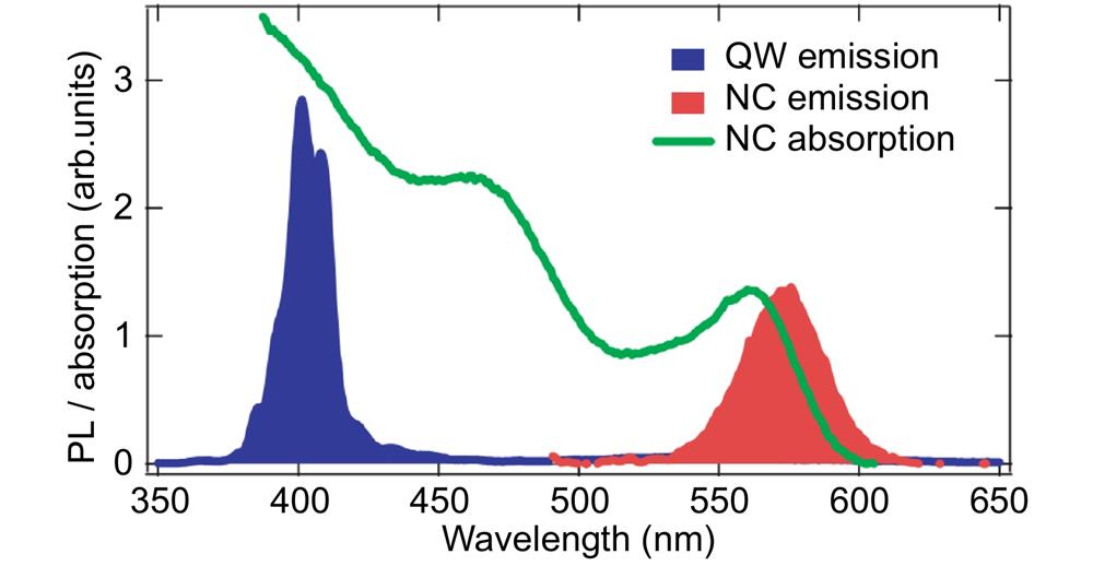
Fig. 2. Optical properties of the hybrid QW/QDs. Figure reproduced with permission from ref.35, Springer Nature.
Fig. 3. (a ) Electroluminescence (EL) wavelength spectrum of a 100 μm × 100 μm AlGaInP micro-LED and (b ) light output power characteristics of 100 μm × 100 μm and 20 μm × 20 μm micro-LEDs with different sidewall treatments. The insets in (a) are EL images of the five micro-LED sizes at 1 A/cm2. Figures reproduced with permission from ref.45, Optical Society of America.
Fig. 4. (a ) PL emission spectra of micro-LEDs with and without ALD passivation. (b ) Temperature-dependent time-resolved photoluminescence decay curves of micro-LEDs with and without ALD. Figures reproduced with permission from ref.46, under a Creative Commons Attribution License.
Fig. 5. (a ) Schematic of the nano-pillar LED. (b ) Cross-sectional SEM image of a nano-pillar LED device. (c ) SEM image of the QD-coated nanopillars. Figures reproduced with permission from ref.28, Optical Society of America.
Fig. 6. Electroluminescence spectra of the (a ) nano-pillar LED and (b ) planar control samples with and without QD coupling. (c ) Time-resolved photoluminescence decay curves of a nano-pillar LED sample with and without QD-coating. Figures reproduced with permission from ref.28, Optical Society of America.
Fig. 7. (a ) Schematic representation, (b ) cross-sectional, and (c ) top SEM images of a photonic quasicrystal LED hybridized with QD color converters. Figures reproduced with permission from ref.50, under a Creative Commons Attribution License.
Fig. 8. Electroluminescence spectra of a PQC LED before (black solid line) and after hybridization (red solid line) with (a ) QD-585 and (b ) a blend of QD-535, QD-585, and QD-630, along with the absorption spectrum of QD-585 (orange dashed line) in (a) and the absorption spectrum of QD-535 (green dashed line), QD-585 (orange dashed line), and QD-630 (red dashed line) in (b). (c , d ) Effective quantum yield (red solid circles) and effective color conversion efficiency (black open squares) of a PQC LED hybridized with QD-585 in (c) and with the QD blend in (d). Figures reproduced with permission from ref.50, under a Creative Commons Attribution License.
Fig. 9. (a ) Schematic diagrams of hybrid h-LED. (b ) Bird’s eye view SEM image of ordered nano-hole arrays in the absence of QDs with ITO current spreading layer on the surface. (c ) Cross-sectional view SEM image of nano-holes filled with NCs, and (d ) transmission electron microscopy (TEM) image of CdSe/ZnS core/shell QDs and a high-resolution image in the inset. Figures reproduced with permission from ref.51, John Wiley and Sons.
Fig. 10. The physical schematic diagram of an NRET process. Figures reproduced with permission from ref.51, John Wiley and Sons.
Fig. 11. (a ) Epitaxial wafer. (b ) Three subpixels of a green micro-LED, a blue micro-LED, and a QD-micro-LED. (c ) Deposition of transparent conducting oxide (TCO) film and P/N electrodes. (d ) Covering distributed Bragg reflector (DBR) filter. (e ) Full-color display panel composed of the proposed hybrid QD-micro-LED. (f ) Cross-sectional view of a single RGB pixel. Figures reproduced with permission from ref.46, Chinese Laser Press.
Fig. 12. (a ) SEM image of RGB pixel array. (b ) SEM image of QD-micro-LED with 30° tilt angle. (c ) TEM image of the contact area between multi-QWs and QDs. (d ) TEM image of 1 nm Al2O3 deposited on the sidewall of an QD-micro-LED through ALD. Figures reproduced with permission from ref.46, Chinese Laser Press.
Fig. 13. (a ) Absorption spectrum of red QD and EL spectrum of blue nano-ring micro-LED. (b ) TRPL curves of nano-ring micro-LED with and without red QDs. (c ) Normalized EL spectra of RGB hybrid full-color micro-LED devices. (d ) Color gamut of RGB hybrid full-color micro-LED device, NTSC, and Rec. 2020. Figures reproduced with permission from ref.46, Chinese Laser Press.
|
Table 1. Luminous performance of LED device based mainly radiative energy transfer or NRET.


Set citation alerts for the article
Please enter your email address

© Copyright 2018-2021 | Chinese Laser Press. All Rights Reserved 沪ICP备15018463号-20