
Xiaotong Fan, Tingzhu Wu, Bin Liu, Rong Zhang, Hao-Chung Kuo, Zhong Chen. Recent developments of quantum dot based micro-LED based on non-radiative energy transfer mechanism[J]. Opto-Electronic Advances, 2021, 4(4): 210022-1
- Opto-Electronic Advances
- Vol. 4, Issue 4, 210022-1 (2021)
Abstract
Keywords
Introduction
Display technology has gone through countless changes and penetrated every corner of our life. As a display technology, light-emitting diode (LED) has attracted attention due to its low cost, easy fabrication, and energy conservation
The RGB full-color display has been employed widely
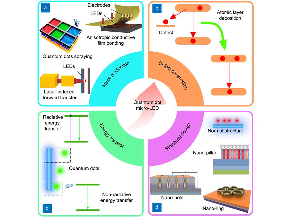
However, technology based on RGB micro-LEDs has serious disadvantages in mass production. For example, to make 4K resolution displays, it is necessary to assemble and drive nearly 25 million micro-LEDs in an economical and efficient way, with a placement accuracy of less than 1 μm. It is very difficult to transfer or grow three different micro-LEDs in such large quantities on the same substrate. As shown in Fig. 1(a), several methods including laser-induced forward transfer and anisotropic conductive film bonding are utilized to help mass transfer
![]()
Figure 1.
To avoid the use of mass transfers, the color conversion scheme of quantum dot (QD) has been proposed
Through hybridization of different QD combinations, it is quite convenient to adjust white light parameters, including the chromaticity coordinates, correlated color temperature, and color rendering index. A hybrid white LED using QDs as down-conversion materials was previously demonstrated by Chen et al.
To achieve excellent luminous properties, it is very important to realize an efficient combination and energy transfer of chips and emitters. Sidewall defects seriously restrict the transfer between micro-LED and QDs, hence, defect passivation of micro-LED is necessary, as shown in Fig. 1(b), atomic layer deposition (ALD) as a suitable method has been reported
Non-radiative energy transfer
Unlike traditional fluorescence conversion, the NRET mechanism is realized through the coupling between dipoles. This function is directly completed at one time through the non-radiative resonance form and does not involve the absorption and conversion of photons. The reemission process reduces the energy loss caused by these indirect processes and can significantly improve the CCE even quantum yield (QY)
| Reference | Performance | Radiative energy transfer | Non-radiative energy transfer |
| Ref. | Quantum yield | 55% | 95% |
| Ref. | Quantum yield | 20% | 55% |
| Ref. | Color conversion efficiency | 3.5% | 13% |
| Ref. | Effective quantum yield | 56.0% | 81.2% |
Table 1.
The NRET mechanism mainly depends on three conditions
Achermann et al. discussed the NRET mechanism between semiconductors with an epitaxial quantum well (QW)
![]()
Figure 2.
To directly prove the NRET process, the time-resolved photoluminescence (TRPL) measurements are essential. The authors tested the change in the delay time of QW under different conditions. The QW delay shortened with the increase in the QD content, indicating an additional relaxation channel for QW excitation, which was believed to have been rooted out of NRET from QW to QDs. More evidence for efficient NRET from QW to QDs was provided by the photoluminescence intensity of QDs. At the same excitation density, the QDs with QW had higher intensity, indicating that NRET promoted an increase in luminescence.
Researchers have proposed a schematic of NRET along with other relaxation processes in the QW/QD structure. After excitation, carrier thermalization, and cooling, the thermal distribution of free electrons and holes was established in QW. QW carriers could decay either radiatively (time constant τrr), non-radiatively (τnr), or experience energy transfer (τET) into QDs. Excitons generated in the QDs by NRET had significant access energies as measured with respect to the bandgap of QDs. In QDs, extremely fast band relaxation (sub-picosecond time scales) can quickly eliminate the resonance between carriers and QW transitions and prevent reverse transfer. In the well-passivated QDs, the relaxed electron hole pairs were mainly recombined by radiation with a time constant of ~20 ns. The non-radiative energy transfer efficiency from QW to QDs could be estimated using the following expression:
where τr is the relaxation time of the QW excitation caused by radiative and non-radiative processes.
Several studies have also reported that NRET improves the luminescence quality of QDs. Achermann et al. discussed the CCE with NRET in another development
where kET is the theoretical energy transfer rate between QW and QDs,
They estimated that CdSe/ZnS core/shell QDs excited by photoluminescence modes could result in approximately 3.5% CCE. However, the measured CCE was 13% when QDs were excited through a mechanism based on absorption–reemission. Taking into account the potential contribution from absorption remission, the CCE produced by the NRET process in the single-QDs-layer structures could be estimated at approximately 10%.
NRET is also expected to play a role in improving the thermal stability. According to the study of Lagoudakis et al., TRPL of QW increased with temperature because of the temperature dependence on other non-radiative recombination channels
Because NRET requires close contact between the donor and the acceptor, the interface of the LED chip is extremely demanding. The photoelectric characteristics of the rectangular-structured micro-LED caused by sidewall defects deteriorate with the shrinking of the chip size, which is more obvious for nano-structured micro-LEDs. Therefore, it is necessary to study the mechanism, rules, and solutions of the impact of sidewall defects on the luminescence performance of micro-LEDs. Tian et al. and Olivier et al. started several studies on this
Using ALD technology to passivate the sidewall of micro-LED chips is an effective way to reduce the adverse effects of sidewall defects on chip performance
Recently, Wong et al. compared the optimization of sidewall defects for red micro-LED devices of different sizes
![]()
Figure 3.(
In addition, the film deposited by ALD possesses good compactness, uniformity, and conformality, and has a good barrier effect on the diffusion of gas and liquid. The QD structure is usually damaged easily by high temperature and humidity. Encapsulating and protecting QDs from water and oxygen is one of the key factors to improving the stability of QDs. Using ALD to form a passivation layer on the surface of QDs is a simple and effective way. Because oxidants (such as water, ozone, hydrogen peroxide, etc.) are commonly used in ALD, which will directly react with the QDs, Kim and Martinson used an anhydrous ALD preparation process, using aluminum isopropoxide and acetic acid as precursors in QDs
Wu et al. reported that Al2O3 passivation could significantly enhance the luminous efficiency of micro-LEDs
![]()
Figure 4.
Novel structures of micro-LED
A shorter distance between the donor and acceptor is important for efficient NRET. According to the report of H. Sahoo
Nano-pillar micro-LED
An earlier attempt has been made by utilizing the nano-pillar heterostructure. Xu et al. reported a novel InGaN/GaN multi-QW nano-pillar LED combined with CdSe/ZnS QDs
![]()
Figure 5.(
The nano-pillar LEDs were fabricated by inductively coupled plasma (ICP) etching with In3Sn nanodots as the etching mask. The method was as follows. First, a SiO2 layer was deposited on the upper surface of the LED chip by plasma-enhanced chemical vapor deposition (PECVD), and an indium tin oxide (ITO) layer was deposited onto the SiO2 layer by electron beam evaporation. The samples were then immersed in a 3% HCl solution to dissolve the ITO phase, leaving self-assembled In3Sn clusters on the SiO2 layer. Next, the In3Sn clusters were used as the etching mask, and the SiO2 layer was etched by a fluoride process. Finally, a patterned SiO2 hard mask was used to dry etch the LED wafer to form an InGaN/GaN nano-pillar heterostructure. By controlling the size of the In3Sn clusters and ICP etching conditions, nanopillars of 200 nm diameter and 50% filling factor were successfully fabricated. The etching depth of 0.6 μm was designed to achieve the n-type layer of the LED heterojunction, and the emissive QWs were exposed laterally along the sidewall of the nanopillars. Figure 5(b) shows the scanning electron microscope (SEM) image of the nano-pillar heterostructure.
After the formation of the nanopillar structure, buffer oxide etching was used to peel off the oxide hard mask, and a Ti/Al (5/200 nm) contact surface was formed at the bottom of the nanopillar to form an n-type electrode. To form a p-type electrode, a p-GaN surface or ITO deposited on p-type GaN was used as the electrode. Finally, a layer of colloidal CdSe/CdS core-shell QDs centered at 620 nm was deposited on the surface of the nanopillar by soaking the device in a solution of QDs for approximately 12 h. Figure 5(c) shows the SEM image of the QD-coated nanopillars, confirming the conformal deposition of QDs on the side wall of the nanopillar structure.
The out spectra of a nanopillar LED prior to and after QD deposition are illustrated in Fig. 6(a). The out spectra of a control sample, prepared by depositing QDs on the upper surface of a planar LED structure, are illustrated in Fig. 6(b). Comparing the two samples, the QDs contained on the nano-pillar LED possessed stronger luminescence than those contained the planar LED. The effective quantum yield (EQY) of QDs was calculated as 43.6% and 12.0% from the data of Fig. 6(a) and Fig. 6(b), respectively. In this study, the EQY is calculated according to the following express:
![]()
Figure 6.Electroluminescence spectra of the (
where Area1 is the reduced integral spectral area of QW after hybridization, Area2 is the integral spectral area of QD emission.
The authors believed that the EQY of QDs on nano-pillar LEDs was increased by 263%. Because the EQY of QDs did not show any dependence on the substrate morphology, the significant improvement in EQY could only be explained by the substantial NRET between QDs and QWs on the side walls of the nano pillars.
Furthermore, TRPL was used to confirm the existence of NRET. As shown in Fig. 6(c), a decay life of approximately 150 ps was measured in the nano pillars without QDs, while the lifetime of QDs deposited on the surface of the nanopillars decreased to 125 ps, indicating that with the existence of QDs, the carrier decay in InGaN QW was faster. Since the deposition of QDs could not change the intrinsic carrier dynamics of InGaN QW, the faster decay meant that a relaxation channel was added to the carriers, which could only be the NRET from QW to QDs.
Nano-hole micro-LED
Nano holes are also considered to be beneficial for realizing NRET. Lagoudakis et al. carried out the opening and etching of the periodic nano-hole array on the surface of an LED chip, depositing QDs in the hole so that the QW and QDs can directly contact
Figure 7(a) shows that the device was a GaN/InGaN multi-QW LED based on a sapphire substrate. To prepare nano-hole LEDs, the following methods were utilized. A GaN nucleation layer, undoped GaN buffer layer, Si-doped n-GaN layer, 10 pairs of In0.21Ga0.79N/GaN multi-QWs with peak wavelengths of 453 nm, and a MgO-doped p-GaN layer were deposited on a sapphire substrate using a bottom-up method. After the growth of the LED wafer, a transparent conductive layer ITO was formed on the wafer surface by electron beam evaporation. Nanoimprint lithography and lithography techniques were used to define nano-holes in selected mesa areas. First, a 400 nm thick SiO2 layer was deposited on the surface of the LED wafer by PECVD, and then a 360 nm thick imprinted resist layer was spin-coated onto the SiO2 layer. By placing and releasing the nanoimprint mold on the infrared layer, the nano-hole pattern of 12 photonic quasicrystals (PQCs) was transferred to the infrared layer. SiO2 nano-holes were prepared by two-step plasma reactive ion etching using O2 and CHF3 processes. The photoresist layer was deposited on the SiO2 layer, and the selected dry etching area was determined using standard lithography technology. LED chips with a photoresist layer and a nano-patterned dielectric layer were etched by inductively coupled plasma reactive ion etching.
![]()
Figure 7.(
This highly symmetric quasicrystal has long-range ordering, short-range disorder, and semi randomness. Because of its highly symmetrical far-field beam shape and the relative increase in state density (which greatly increased the extraction of light), this geometry has been proven to be far superior to conventional PQC lattices commonly used in LED applications. The spin coating parameters were adjusted to allow the QDs to completely fill the nano-holes, as shown in Figs. 7(b) and 7(c). The LEDs were etched to induce a shunt path, and a non-radiative recombination center was formed by a bond suspended on the side wall.
The single-color converter was hybridized with QDs with an emission wavelength of 585 nm. Figure 8(a) shows the electroluminescence (EL) spectrum of the hybrid (black solid line) and the absorption spectrum (orange dashed line) of QDs before (black solid line) and after (red solid line) hybridization. White LEDs were made of a mixture of green, orange, and red QDs. Figure 8(b) shows the EL spectra of the PQC LED and QD before and after hybridization with QDs as well as the absorption spectra of different QD colors (green, orange, and red dashed lines). There was a strong spectral overlap between the absorption of different QDs and LEDs, which is a prerequisite for effective energy transfer between QWs and QDs. A relatively narrow (full width of half maximum is about 30 nm) luminescence was observed in the mixed electroluminescence spectrum. In the case of single-color QDs and hybrid QDs, it was found that the QDs strongly quenched the EL maximum of the LED, which indicated that there was a significant energy transfer between the QW and the QDs.
![]()
Figure 8.Electroluminescence spectra of a PQC LED before (black solid line) and after hybridization (red solid line) with (
Figures 8(c) and 8(d) show the CCE and EQY as a function of the injection current of the single-color LED and white LED, respectively. They were both much higher than the results of previous reports. The maximum values of CCE of the single-color LED and white LED were 66.7% and 70%, respectively. Here, CCE is defined as the ratio of integral spectral area of QD emission after hybridisation to integral spectral area of blue LED before hybridization. It is believed that the increase results from the fact that the QDs were fully filled into nano-holes.
The maximum EQYs of the single-color LED and white LED were 110% and 123%, respectively. Since EQY is determined by ratio of photon counts rather photon energy of emission and absorption, the value could be large than 100% during down conversion luminescence. The increase resulted from the NRET mechanism connecting the PQC LED chip to QDs, and the conclusion was proved by the TRPL curves, in which the lifetimes of the PQC LED chips decreased after combining with QDs.
Zhang et al. have also prepared a new type of hybrid nano-hole periodic array/II-VI group white light LED device
Figure 9(a) shows a schematic diagram of the designed hybrid LED. To achieve good current diffusion, an ITO layer was deposited on the LED surface and patterned as a nano-hole. Figure 9(b) shows that the nano-hole arrays with a diameter of 300 nm were arranged in hexagonal lattices with a lattice constant of 600 nm. Then, CdSe/ZnS core-shell nanocrystals were filled into these nano-holes as a down-conversion medium. This structure ensured that the core/shell nanocrystals of CdSe/ZnS were located near the active multi-QWs. Figure 9(c) shows the cross-section of the hybrid device at a depth of approximately 1.2 μm. The side walls of the InGaN/GaN multi-QWs were tightly surrounded by the expected nanocrystals, which was crucial for the NRET process. Figure 9(d) shows the CdSe/ZnS core–shell nanocrystals with diameters less than 10 nm. In this study, there was no change in the I-V curve after nanocrystals were dripped onto the h-LED, indicating that nanocrystals had no effect on the injection of electrons and holes.
![]()
Figure 9.(
In addition, the effective QY was calculated. For yellow (546 nm) nanocrystals, the effective quantum yields were 94% and 83% in the violet and blue LEDs, respectively, which were even higher than those of the YAG: Ce phosphor. This contributed to the NRET process. Figure 10 illustrates the NRET process between the multi-QWs and nanocrystals along with the relaxation process in the hybrid LED. Because of this geometry, the excitons in multi-QWs were coupled with the 2D assembly of nanocrystals (NCs), which acted as a one-dimensional confined structure. As the figure shows, carriers were generated by optical pumping or current injection, and excitons were distributed in multi-QWs. If the exciton energy of multi-QWs matched with the absorption energy of NCs, these excitons could emit photons by radiation, recombine non-radiatively through defects, or undergo NRET to form the NCs components. When the energy was transferred to NCs, in-band relaxation would occur immediately, thus eliminating the resonance between the exciton and multi-QW transition and effectively preventing the reverse transfer process. Then, the relaxation excitons in NCs recombine (mainly in the form of radiation) and emit photons whose energy corresponds to the band gap of NCs.
![]()
Figure 10.
Nano-ring micro-LED
Due to that the nano-hole structure only exposes the chip QW on the inner side of the hole wall and the nano-ring structure can expose the QW on both the inner and outer sides of the ring wall, the surface area of the chip QW in direct contact with the QDs can be increased. The proportion of NRET mechanisms in the color conversion process of QDs can also be significantly increased.
Kuo et al. used nanosphere pattern transfer technology to prepare a large area of nano-ring LED arrays with a diameter of less than 1 μm on a green epitaxial wafer
Using a similar method, Wu et al. reported the use of a nano-ring micro-LED for full-color display
![]()
Figure 11.(
The manufactured QD-micro-LED was studied using SEM. Figures 12(a) and 12(b) show the SEM images with different scales and perspectives. In addition, from the transmission electron microscopy (TEM) image in Fig. 12(c), it can be clearly observed that the sidewalls of the InGaN/GaN MQW were closely surrounded by QDs, which was essential for the NRET mechanism. Red QDs with a diameter of about 10 nm were also observed. In addition, it can be seen in the TEM image of Fig. 12(d) that a 1 nm thick Al2O3 layer was deposited on the sidewall of the QD-micro-LED.
![]()
Figure 12.(
In this work, the red QDs were in close contact with the blue-emission multi-QWs of nano-ring LEDs so that the red QDs could be excited efficiently. According to the wide overlap of the absorption spectrum of the red QDs and the electroluminescence spectrum of the multi-QWs shown in Fig. 13(a), it was possible for NRET to exist between QDs and QWs. The TRPL curves of the QWs further confirmed NRET, as the QWs’ contact with QDs possessed a shorter lifetime. The results of TRPL are displayed in Fig. 13(b). The lifetime of QWs decreased 1.12 ns after encapsulation with QDs, and the efficiency of NRET was calculated as 53.6%. Figures 13(c) and 13(d) shows that, after structural design and spring painting, the epitaxial wafer could emit RGB light with a narrow half-width, with peak wavelengths located at 630 nm, 525 nm, and 467 nm, respectively. The color gamut overlap of the NTSC space was approximately 104.8% and that of Rec. 2020 was 78.2%. These results indicated that the nano-ring micro-LEDs based on the NRET mechanism was sufficient to support full-color performance in display technology.
![]()
Figure 13.(
Challenges and perspectives
As a solution, NRET plays a significant role in improving the luminous properties of QD-based micro-LEDs. According to the review, the overlap of the emission spectrum of the donor (QW) and the absorption spectrum of the acceptor (QD) as well as the sufficiently short (less than 10 nm) distance between the QW and QD are important for promoting the NRET process. Nano-pillar, nano-hole, and nano-ring structures have been studied to achieve a close contact between the QW and QD, so that NRET occupies more components in the process of energy transfer. These results both improve the EQY and CCE, which will be beneficial to the improvement of display performance.
However, several problems remain to be solved. First, more stable and brighter full-color QDs are necessary to support the NRET process, which is the source of the problem. Researchers usually use the method of encapsulating organic ligands to improve the stability of QD. However, the tolerance of organic ligands to high temperature and chemical environment is poor, which limits the application of QD. Recently, the study of perovskite QD encapsulated by molecular sieve structures has attracted increasing attention
Although a variety of nanostructures have been designed, none of the current structures are perfect. For example, although nano-ring LED exposes more QWs, which increases the efficiency of NRET between QWs and QDs, the light output direction of the exposed QDs is not vertical outward but lateral, which results in low light output of the whole system and restricts the practical application. Therefore, it is necessary to design greater LED structures to improve the luminescent performance of the whole system.
With the advent of 5G and Sub 6G, visible light communication is preparing for the next generation of communication technology. Visible light communication uses LED as the light source, and can be used with indoor lighting, electronic Kanban, and display as a means of wireless communication. However, the traditional large size LED light source can only reach the frequency of tens of MHz, and there is still much room for improvement. Therefore, in addition to its application in the display, micro-LED will also have great potential in visible light communication due to its high modulation bandwidth
References
[1] P Pust, PJ Schmidt, W Schnick. A revolution in lighting. Nat Mater, 14, 454-458(2015).
[2] S Reineke. Complementary LED technologies. Nat Mater, 14, 459-462(2015).
[3] HX Jiang, SX Jin, J Li, J Shakya, JY Lin. III-nitride blue microdisplays. Appl Phys Lett, 78, 1303-1305(2001).
[4] SX Jin, J Li, JY Lin, HX Jiang. InGaN/GaN quantum well interconnected microdisk light emitting diodes. Appl Phys Lett, 77, 3236-3238(2000).
[5] SX Jin, J Li, JZ Li, JY Lin, HX Jiang. GaN microdisk light emitting diodes. Appl Phys Lett, 76, 631-633(2000).
[6] TZ Wu, CW Sher, Y Lin, CF Lee, F Liang, et al. Mini-LED and micro-LED: promising candidates for the next generation display technology. Appl Sci, 8, 1557(2018).
[7] ZJ Liu, CH Lin, BR Hyun, CW Sher, ZJ Lv, et al. Micro-light-emitting diodes with quantum dots in display technology. Light Sci Appl, 9, 83(2020).
[8] YM Yin, ZP Hu, MU Ali, M Duan, L Gao, et al. Full-color micro-LED display with CsPbBr3 perovskite and CdSe quantum dots as color conversion layers. Adv Mater Technol, 5, 2000251(2020).
[9] YG Huang, EL Hsiang, MY Deng, ST Wu. Mini-LED, micro-LED and OLED displays: present status and future perspectives. Light Sci Appl, 9, 105(2020).
[10] XJ Zhou, PF Tian, CW Sher, J Wu, HZ Liu, et al. Growth, transfer printing and colour conversion techniques towards full-colour micro-LED display. Prog Quant Electron, 71, 100263(2020).
[11] YJ Hong, CH Lee, A Yoon, M Kim, HK Seong, et al. Visible-color-tunable light-emitting diodes. Adv Mater, 23, 3284-3288(2011).
[12] SWH Chen, YM Huang, KJ Singh, YC Hsu, FJ Liou, et al. Full-color micro-LED display with high color stability using semipolar (20-21) InGaN LEDs and quantum-dot photoresist. Photonics Res, 8, 630-636(2020).
[13] FW Gou, EL Hsiang, GJ Tan, YF Lan, CY Tsai, et al. Tripling the optical efficiency of color-converted micro-LED displays with funnel-tube array. Crystals, 9, 39(2019).
[14] CK Jeong, KI Park, JH Son, GT Hwang, SH Lee, et al. Self-powered fully-flexible light-emitting system enabled by flexible energy harvester. Energy Environ Sci, 7, 4035-4043(2014).
[15] K Ding, V Avrutin, N Izyumskaya, Ü Özgür, H Morkoç. Micro-LEDs, a manufacturability perspective. Appl Sci, 9, 1206(2019).
[16] K Wang, YX Du, J Liang, JY Zhao, FF Xu, et al. Wettability-guided screen printing of perovskite microlaser arrays for current-driven displays. Adv Mater, 32, 2001999(2020).
[17] WH Mei, ZQ Zhang, AD Zhang, D Li, XY Zhang, et al. High-resolution, full-color quantum dot light-emitting diode display fabricated via photolithography approach. Nano Res, 13, 2485-2491(2020).
[18] Y Shirasaki, GJ Supran, MG Bawendi, V Bulović. Emergence of colloidal quantum-dot light-emitting technologies. Nat Photonics, 7, 13-23(2013).
[19] SJ Ho, HC Hsu, CW Yeh, HS Chen. Inkjet-printed salt-encapsulated quantum dot film for UV-based RGB color-converted micro-light emitting diode displays. ACS Appl Mater Interfaces, 12, 33346-33351(2020).
[20] T Kim, KH Kim, S Kim, SM Choi, H Jang, et al. Efficient and stable blue quantum dot light-emitting diode. Nature, 586, 385-389(2020).
[21] H Sekiguchi, K Kishino, A Kikuchi. Emission color control from blue to red with nanocolumn diameter of InGaN/GaN nanocolumn arrays grown on same substrate. Appl Phys Lett, 96, 231104(2010).
[22] HY Lin, CW Sher, DH Hsieh, XY Chen, HMP Chen, et al. Optical cross-talk reduction in a quantum-dot-based full-color micro-light-emitting-diode display by a lithographic-fabricated photoresist mold. Photonics Res, 5, 411-416(2017).
[23] HS Chen, CK Hsu, HY Hong. InGaN-CdSe-ZnSe quantum dots white LEDs. IEEE Photon Technol Lett, 18, 193-195(2006).
[24] BZ Zhou, MJ Liu, YW Wen, Y Li, R Chen. Atomic layer deposition for quantum dots based devices. Opto-Electron Adv, 3, 190043(2020).
[25] JJ Rindermann, G Pozina, B Monemar, L Hultman, H Amano, et al. Dependence of resonance energy transfer on exciton dimensionality. Phys Rev Lett, 107, 236805(2011).
[26] AR Clapp, IL Medintz, H Mattoussi. Förster resonance energy transfer investigations using quantum-dot fluorophores. Chemphyschem, 7, 47-57(2006).
[27] HV Han, HY Lin, CC Lin, WC Chong, JR Li, et al. Resonant-enhanced full-color emission of quantum-dot-based micro LED display technology. Opt Express, 23, 32504-32515(2015).
[28] F Zhang, J Liu, GJ You, CF Zhang, SE Mohney, et al. Nonradiative energy transfer between colloidal quantum dot-phosphors and nanopillar nitride LEDs. Opt Express, 20, A333-A339(2012).
[29] S Chanyawadee, PG Lagoudakis, RT Harley, MDB Charlton, DV Talapin, et al. Increased color-conversion efficiency in hybrid light-emitting diodes utilizing non-radiative energy transfer. Adv Mater, 22, 602-606(2010).
[30] SW Wang, KB Hong, YL Tsai, CH Teng, AJ Tzou, et al. Wavelength tunable InGaN/GaN nano-ring LEDs via nano-sphere lithography. Sci Rep, 7, 42962(2017).
[31] G Itskos, G Heliotis, PG Lagoudakis, J Lupton, NP Barradas, et al. Efficient dipole-dipole coupling of Mott-Wannier and Frenkel excitons in (Ga, In)N quantum well/polyfluorene semiconductor heterostructures. Phys Rev B, 76, 035344(2007).
[32] Š Kos, M Achermann, VI Klimov, DL Smith. Different regimes of Förster-type energy transfer between an epitaxial quantum well and a proximal monolayer of semiconductor nanocrystals. Phys Rev B, 71, 205309(2005).
[33] IL Medintz, AR Clapp, JS Melinger, JR Deschamps, H Mattoussi. A reagentless biosensing assembly based on quantum dot-donor Förster resonance energy transfer. Adv Mater, 17, 2450-2455(2005).
[34] G Heliotis, G Itskos, R Murray, MD Dawson, IM Watson, et al. Hybrid inorganic/organic semiconductor heterostructures with efficient non-radiative energy transfer. Adv Mater, 18, 334-338(2006).
[35] M Achermann, MA Petruska, S Kos, DL Smith, DD Koleske, et al. Energy-transfer pumping of semiconductor nanocrystals using an epitaxial quantum well. Nature, 429, 642-646(2004).
[36] M Achermann, MA Petruska, DD Koleske, MH Crawford, VI Klimov. Nanocrystal-based light-emitting diodes utilizing high-efficiency nonradiative energy transfer for color conversion. Nano Lett, 6, 1396-1400(2006).
[37] JV Vaghasiya, KK Sonigara, L Suresh, M Panahandeh-Fard, SS Soni, et al. Efficient power generating devices utilizing low intensity indoor lights via non-radiative energy transfer mechanism from organic ionic redox couples. Nano Energy, 60, 457-466(2019).
[38] H Sahoo. Förster resonance energy transfer – a spectroscopic nanoruler: principle and applications. J Photochem Photobiol C, 12, 20-30(2011).
[39] C Krishnan, T Mercier, T Rahman, G Piana, M Brossard, et al. Efficient light harvesting in hybrid quantum dot-interdigitated back contact solar cells
[40] PF Tian, JJD McKendry, Z Gong, B Guilhabert, IM Watson, et al. Size-dependent efficiency and efficiency droop of blue InGaN micro-light emitting diodes. Appl Phys Lett, 101, 231110(2012).
[41] F Olivier, A Daami, C Licitra, F Templier. Shockley-read-hall and auger non-radiative recombination in GaN based LEDs: a size effect study. Appl Phys Lett, 111, 022104(2017).
[42] IS Kim, ABF Martinson. Stabilizing hybrid perovskites against moisture and temperature
[43] JP Richters, T Voss, DS Kim, R Scholz, M Zacharias. Enhanced surface-excitonic emission in ZnO/Al2O3 core-shell nanowires. Nanotechnology, 19, 305202(2008).
[44] MS Wong, D Hwang, AI Alhassan, C Lee, R Ley, et al. High efficiency of III-nitride micro-light-emitting diodes by sidewall passivation using atomic layer deposition. Opt Express, 26, 21324-21331(2018).
[45] MS Wong, JA Kearns, C Lee, JM Smith, C Lynsky, et al. Improved performance of AlGaInP red micro-light-emitting diodes with sidewall treatments. Opt Express, 28, 5787-5793(2020).
[46] Chen Huang, CC Shen, TZ Wu, ZY Liao, LF Chen, et al. Full-color monolithic hybrid quantum dot nanoring micro light-emitting diodes with improved efficiency using atomic layer deposition and nonradiative resonant energy transfer. Photonics Res, 7, 416-422(2019).
[47] CY Liu, TP Chen, TS Kao, JK Huang, HC Kuo, et al. Color-conversion efficiency enhancement of quantum dots via selective area nano-rods light-emitting diodes. Opt Express, 24, 19978-19987(2016).
[48] S Ghataora, RM Smith, M Athanasiou, T Wang. Electrically injected hybrid organic/inorganic III-nitride white light-emitting diodes with nonradiative Förster resonance energy transfer. ACS Photonics, 5, 642-647(2018).
[49] JH Kang, BJ Li, TS Zhao, MA Johar, CC Lin, et al. RGB arrays for micro-light-emitting diode applications using nanoporous GaN embedded with quantum dots. ACS Appl Mater Interfaces, 12, 30890-30895(2020).
[50] C Krishnan, M Brossard, KY Lee, JK Huang, CH Lin, et al. Hybrid photonic crystal light-emitting diode renders 123% color conversion effective quantum yield. Optica, 3, 503-509(2016).
[51] Z Zhuang, X Guo, B Liu, FR Hu, Y Li, et al. High color rendering index hybrid III-nitride/nanocrystals white light-emitting diodes. Adv Funct Mater, 26, 36-43(2016).
[52] QG Zhang, B Wang, WL Zheng, L Kong, Q Wan, et al. Ceramic-like stable CsPbBr3 nanocrystals encapsulated in silica derived from molecular sieve templates. Nat Commun, 11, 31(2020).

Set citation alerts for the article
Please enter your email address
© Copyright 2018-2021 | Chinese Laser Press. All Rights Reserved 沪ICP备15018463号-20