• Opto-Electronic Engineering
  • Vol. 50, Issue 3, 220133 (2023)
Shunhua Yang1, Chenliang Ding1、*, Dazhao Zhu1, Zhenyao Yang1, Yong Liu1、3, Cuifang Kuang1、2、4、**, and Xu Liu1、2
Author Affiliations
  • 1Research Center for Intelligent Chips and Devices, Zhejiang Lab, Hangzhou, Zhejiang 311121, China
  • 2State Key Laboratory of Extreme Photonics and Instrumentation, College of Optical Science and Engineering, Zhejiang University, Hangzhou, Zhejiang 310027, China
  • 3College of Electronics and Information Engineering, Shanghai University of Electric Power, Shanghai 200090, China
  • 4ZJU-Hangzhou Global Scientific and Technological Innovation Center, Hangzhou, Zhejiang 311200, China
  • show less
    DOI: 10.12086/oee.2023.220133 Cite this Article
    Shunhua Yang, Chenliang Ding, Dazhao Zhu, Zhenyao Yang, Yong Liu, Cuifang Kuang, Xu Liu. High-speed two-photon lithography based on femtosecond laser[J]. Opto-Electronic Engineering, 2023, 50(3): 220133 Copy Citation Text show less
    Optical methods of improving the TPL throughput. (a) Single-beam writing; (b) Multi-foci parallel lithography; (c) Pattern projection; (d) 3D projection exposure
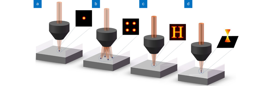
    Fig. 1. Optical methods of improving the TPL throughput. (a) Single-beam writing; (b) Multi-foci parallel lithography; (c) Pattern projection; (d) 3D projection exposure
    The scanning scheme for single-beam writing based on (a) motorized stage, (b) galvo, (c) polygon laser scanner, and (d) acousto-optic deflector (AOD)
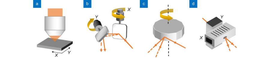
    Fig. 2. The scanning scheme for single-beam writing based on (a) motorized stage, (b) galvo, (c) polygon laser scanner, and (d) acousto-optic deflector (AOD)
    (a) Configuration of the parallel writing system based on diffractive beam splitter (DBS) and multi-beam interference; (b)~(d) The periodic structures written by the foci array generated via the interference of four femtosecond laser beams (800 nm/1 kHz). The exposure time is 30 s, 80 s, and 120 s, respectively; (e)~(g) The dot array structures fabricated by the foci lattice generated via four-beam interference with different interference angles of 10.8°, 21.9°, and 33.6°, respectively; (h) The periodic lattice structure written by the foci array generated via three-beam interference[53-55]
    Fig. 3. (a) Configuration of the parallel writing system based on diffractive beam splitter (DBS) and multi-beam interference; (b)~(d) The periodic structures written by the foci array generated via the interference of four femtosecond laser beams (800 nm/1 kHz). The exposure time is 30 s, 80 s, and 120 s, respectively; (e)~(g) The dot array structures fabricated by the foci lattice generated via four-beam interference with different interference angles of 10.8°, 21.9°, and 33.6°, respectively; (h) The periodic lattice structure written by the foci array generated via three-beam interference[53-55]
    (a) Configuration of the multi-photon writing system based on four-beam interference; (b) Pillar array fabricated by once laser exposure (1 s), period 7.5 μm, height 20 μm, and diameter 3 μm; (c) Large-scale periodic structure fabricated by continuously shifting the once-exposure position of foci array with diameter of ~80 μm[56]
    Fig. 4. (a) Configuration of the multi-photon writing system based on four-beam interference; (b) Pillar array fabricated by once laser exposure (1 s), period 7.5 μm, height 20 μm, and diameter 3 μm; (c) Large-scale periodic structure fabricated by continuously shifting the once-exposure position of foci array with diameter of ~80 μm[56]
    Femtosecond laser parallel direct writing system based on MLA. (a) Direct writing using MLA foci array; (b) Multi-foci writing by imaging the MLA foci array to the focal plane of the objective[63-64]
    Fig. 5. Femtosecond laser parallel direct writing system based on MLA. (a) Direct writing using MLA foci array; (b) Multi-foci writing by imaging the MLA foci array to the focal plane of the objective[63-64]
    (a) The overall appearance and optical microscopic image of MLA; (b) SEM of the photopolymerized resin voxels on glass substrate; (c) The 2D array structure of 277 ‘N’ microletters fabricated by 28 foci;(d) The fabricated 3D microspring array[65]
    Fig. 6. (a) The overall appearance and optical microscopic image of MLA; (b) SEM of the photopolymerized resin voxels on glass substrate; (c) The 2D array structure of 277 ‘N’ microletters fabricated by 28 foci;(d) The fabricated 3D microspring array[65]
    (a) SEM of 3D periodic structures coated with silver fabricated on a hydrophobic coated glass surface; (b) Enlarged view of a single uncoated polymerized structure composed of a spring on top of a cube; (c) The polymerized structure of (b) with coated silver[66]
    Fig. 7. (a) SEM of 3D periodic structures coated with silver fabricated on a hydrophobic coated glass surface; (b) Enlarged view of a single uncoated polymerized structure composed of a spring on top of a cube; (c) The polymerized structure of (b) with coated silver[66]
    (a) DBS-based multi-photon processing system with multiple femtosecond laser beams; (b) Multi-foci pattern generated by DBS; (c)~(f) The structures of designed Logo, assembled microgear set (diameter 22 μm), 3D microfans, and assembled microgear set fabricated with the optical setup of (a)[72]
    Fig. 8. (a) DBS-based multi-photon processing system with multiple femtosecond laser beams; (b) Multi-foci pattern generated by DBS; (c)~(f) The structures of designed Logo, assembled microgear set (diameter 22 μm), 3D microfans, and assembled microgear set fabricated with the optical setup of (a)[72]
    DOE-based mluti-beam parallel femtosecond laser writing. (a) SEM of the DOE surface; (b) Enlarged view of (a); (c) Overall appearance of the DOE; (d) Normalized false-color intensity measurement of the DOE using a CMOS-camera; (e) Parallel 3D two-photon fabricating system based on 3×3 foci generated by DOE; (f) Designed model of the chiral 3D metamaterial cubic cell, a=80 μm; (g) 2.4 mm×2.4 mm×9.6 mm chiral metamaterial structure consisting of 30×30×120=108000 3D cubic cells of (f); (h) Oblique side-view SEM of the structure in (g)73]
    Fig. 9. DOE-based mluti-beam parallel femtosecond laser writing. (a) SEM of the DOE surface; (b) Enlarged view of (a); (c) Overall appearance of the DOE; (d) Normalized false-color intensity measurement of the DOE using a CMOS-camera; (e) Parallel 3D two-photon fabricating system based on 3×3 foci generated by DOE; (f) Designed model of the chiral 3D metamaterial cubic cell, a=80 μm; (g) 2.4 mm×2.4 mm×9.6 mm chiral metamaterial structure consisting of 30×30×120=108000 3D cubic cells of (f); (h) Oblique side-view SEM of the structure in (g)73]
    (a) The SLM-based multi-foci femtosecond two-photon lithography system; (b) The Venus sculptures fabricated by 4×4 foci; (c) The scaffold for cell cultivation fabricated by 4 foci; (d) 36 microneedles processed by 4 foci[74]
    Fig. 10. (a) The SLM-based multi-foci femtosecond two-photon lithography system; (b) The Venus sculptures fabricated by 4×4 foci; (c) The scaffold for cell cultivation fabricated by 4 foci; (d) 36 microneedles processed by 4 foci[74]
    (a) The SLM-based multi-foci femtosecond laser parallel writing system; (b)~(c) The hologram loaded in SLM and the generated 7 foci pattern, respectively; (d)~(g) Microlens arrays fabricated by SLM with 3 foci, 7 foci, and 4×4 foci respectively; (h)~(i) The overall image and enlarged view of the 3D woodpile photonic structure fabricated by 10 foci; (j) Illustration of the multi-foci parallel fabrication process with the spiral scanning strategy; (k)~(m) 3D spiral photonic structures of ‘L’, ‘Z’, and ‘H’ fabricated by the multi-beam scanning way of (j). The foci pitch is 5.6 μm and the diameters of scanning spiral are 10 μm, 6 μm, and 8 μm, respectively[75]
    Fig. 11. (a) The SLM-based multi-foci femtosecond laser parallel writing system; (b)~(c) The hologram loaded in SLM and the generated 7 foci pattern, respectively; (d)~(g) Microlens arrays fabricated by SLM with 3 foci, 7 foci, and 4×4 foci respectively; (h)~(i) The overall image and enlarged view of the 3D woodpile photonic structure fabricated by 10 foci; (j) Illustration of the multi-foci parallel fabrication process with the spiral scanning strategy; (k)~(m) 3D spiral photonic structures of ‘L’, ‘Z’, and ‘H’ fabricated by the multi-beam scanning way of (j). The foci pitch is 5.6 μm and the diameters of scanning spiral are 10 μm, 6 μm, and 8 μm, respectively[75]
    (a) Phase modulation scheme based on two synchronized SLMs; (b) Illustration of the 3D PPI array through duplicating the 2×2 parallel PPI foci; (c) The dot array fabricated with femtosecond foci. The blue arrows indicate the scanning route; (d) The dot array fabricated by PPI foci with inhibition power of 210 mW. Scale bar: 500 nm; (e) SEM of the fabricated letters by 2 × 2 PPI foci (left) and the femtosecond multifocal array (right). Each letter is processed respectively by one focus of the 2×2 multifocal array. Scale bars: 1 μm; (f) The scheme for parallelized PPI 3D writing on different layers with interval of 1.5 μm; (g) 3D dots with interval of 200 nm and size of 80 nm on three different layers which are fabricated by the PPI multifocal array [76]
    Fig. 12. (a) Phase modulation scheme based on two synchronized SLMs; (b) Illustration of the 3D PPI array through duplicating the 2×2 parallel PPI foci; (c) The dot array fabricated with femtosecond foci. The blue arrows indicate the scanning route; (d) The dot array fabricated by PPI foci with inhibition power of 210 mW. Scale bar: 500 nm; (e) SEM of the fabricated letters by 2 × 2 PPI foci (left) and the femtosecond multifocal array (right). Each letter is processed respectively by one focus of the 2×2 multifocal array. Scale bars: 1 μm; (f) The scheme for parallelized PPI 3D writing on different layers with interval of 1.5 μm; (g) 3D dots with interval of 200 nm and size of 80 nm on three different layers which are fabricated by the PPI multifocal array [76]
    (a) Illustration of fabricating integrated miniaturized structure inside a ‘Y’ shape microchannel by parallel femtosecond multiple foci; (b)~(g) the structures with patterns of ‘LOC’ characters, ‘Cross’ and ‘Svastika’ fabricated on the substrate surface (b)~(d) and in the channel (e)~(g) respectively[77]
    Fig. 13. (a) Illustration of fabricating integrated miniaturized structure inside a ‘Y’ shape microchannel by parallel femtosecond multiple foci; (b)~(g) the structures with patterns of ‘LOC’ characters, ‘Cross’ and ‘Svastika’ fabricated on the substrate surface (b)~(d) and in the channel (e)~(g) respectively[77]
    (a) The configuration of SLM-based multi-foci parallel writing system for micropillar fabrication. The inset illustrates the design of CGH; (b) The schematic diagram of self-assembly structure formation by capillary force on micropillars; (c)~(e) Diverse micro-assemblies with 6, 8, and 12 micropillars respectively fabricated by foci array with different beam quantity and distribution.Scale bar: 2 μm; (f)~(g) In-situ trapping of microparticles by the micro-assemblies fabricated with six-foci beams[78]
    Fig. 14. (a) The configuration of SLM-based multi-foci parallel writing system for micropillar fabrication. The inset illustrates the design of CGH; (b) The schematic diagram of self-assembly structure formation by capillary force on micropillars; (c)~(e) Diverse micro-assemblies with 6, 8, and 12 micropillars respectively fabricated by foci array with different beam quantity and distribution.Scale bar: 2 μm; (f)~(g) In-situ trapping of microparticles by the micro-assemblies fabricated with six-foci beams[78]
    (a) Optical configuration of DMD-based multi-foci femtosecond laser parallel writing system; (b) Designed laser scanning trajectories, laser writing process, and SEMs of the fabricated woodpile structures with single-focus, two-foci, and three-foci writing respectively. Scale bar: 10 μm[79]
    Fig. 15. (a) Optical configuration of DMD-based multi-foci femtosecond laser parallel writing system; (b) Designed laser scanning trajectories, laser writing process, and SEMs of the fabricated woodpile structures with single-focus, two-foci, and three-foci writing respectively. Scale bar: 10 μm[79]
    (a) Schematic diagram of the DMD-based femtosecond laser projection lithography system; (b) Large-scale periodic microstructures of ‘ORC’ letters fabricated by DMD once projection[80]
    Fig. 16. (a) Schematic diagram of the DMD-based femtosecond laser projection lithography system; (b) Large-scale periodic microstructures of ‘ORC’ letters fabricated by DMD once projection[80]
    (a) Schematic diagram of DMD-based projection system using the spatial and temporal focusing of femtosecond laser; (b) 2.2 mm×2.2 mm×0.25 mm cube supported on a U.S. penny fabricated in 8 min 20 s; (c) Fabricated 3D micropillar stacked with2D layers; (d) Spiral structures through once projection within several millisecond; (e) Overhanging 3D structures[30]
    Fig. 17. (a) Schematic diagram of DMD-based projection system using the spatial and temporal focusing of femtosecond laser; (b) 2.2 mm×2.2 mm×0.25 mm cube supported on a U.S. penny fabricated in 8 min 20 s; (c) Fabricated 3D micropillar stacked with2D layers; (d) Spiral structures through once projection within several millisecond; (e) Overhanging 3D structures[30]
    (a) Schematic diagram of femtosecond laser direct writing. The optical intensity distribution at the focal plane is a round point; (b) Schematic diagram of single-exposure holographic femtosecond laser direct patterning. The optical intensity distribution at the defocused plane is a complex pattern ‘H’ designed by computer generated hologram (CGH). However, the distribution shows low signal-to-noise and leads to low surface quality in fabricating micro/nanostructures; (c) Multiexposure holographic femtosecond laser direct patterning. The optical intensity distribution at the defocused plane is a complex pattern ‘H’ designed by multi-CGH with different phases. Due to the improved strategy, the distribution shows high signal-to-noise and thus high quality micro/nanostructures will be realized[81-82]
    Fig. 18. (a) Schematic diagram of femtosecond laser direct writing. The optical intensity distribution at the focal plane is a round point; (b) Schematic diagram of single-exposure holographic femtosecond laser direct patterning. The optical intensity distribution at the defocused plane is a complex pattern ‘H’ designed by computer generated hologram (CGH). However, the distribution shows low signal-to-noise and leads to low surface quality in fabricating micro/nanostructures; (c) Multiexposure holographic femtosecond laser direct patterning. The optical intensity distribution at the defocused plane is a complex pattern ‘H’ designed by multi-CGH with different phases. Due to the improved strategy, the distribution shows high signal-to-noise and thus high quality micro/nanostructures will be realized[81-82]
    (a) Experimental setup for single exposure fabrication of microtubes; (b) Calculated light intensity distribution at the focal region in the propagation direction; (c) SEM of microtubes[89]
    Fig. 19. (a) Experimental setup for single exposure fabrication of microtubes; (b) Calculated light intensity distribution at the focal region in the propagation direction; (c) SEM of microtubes[89]
    (a) Experimental setup for the fabrication of 3D chiral microstructures by single exposure; (b) The spatial intensity distribution of the modulated beam and the electron microscopy of the writing results[90]
    Fig. 20. (a) Experimental setup for the fabrication of 3D chiral microstructures by single exposure; (b) The spatial intensity distribution of the modulated beam and the electron microscopy of the writing results[90]
    Shunhua Yang, Chenliang Ding, Dazhao Zhu, Zhenyao Yang, Yong Liu, Cuifang Kuang, Xu Liu. High-speed two-photon lithography based on femtosecond laser[J]. Opto-Electronic Engineering, 2023, 50(3): 220133
    Download Citation