
Leonid Yu. Beliaev, Osamu Takayama, Pavel N. Melentiev, Andrei V. Lavrinenko. Photoluminescence control by hyperbolic metamaterials and metasurfaces: a review[J]. Opto-Electronic Advances, 2021, 4(8): 210031-1
- Opto-Electronic Advances
- Vol. 4, Issue 8, 210031-1 (2021)
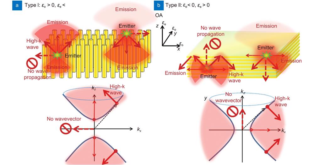
Fig. 1. Schematic illustration of hyperbolic metamaterials and metasurfaces. (a ) Type I hyperbolic metamaterials (ε o > 0 and ε e < 0) in metallic nanorod or nanowire configuration and their representative dispersion in the wavevector space (k-space). ( b ) Type II hyperbolic metamaterials (ε o < 0 and ε e > 0) in metal-dielectric multilayer configuration and their dispersion in the wavevector space.
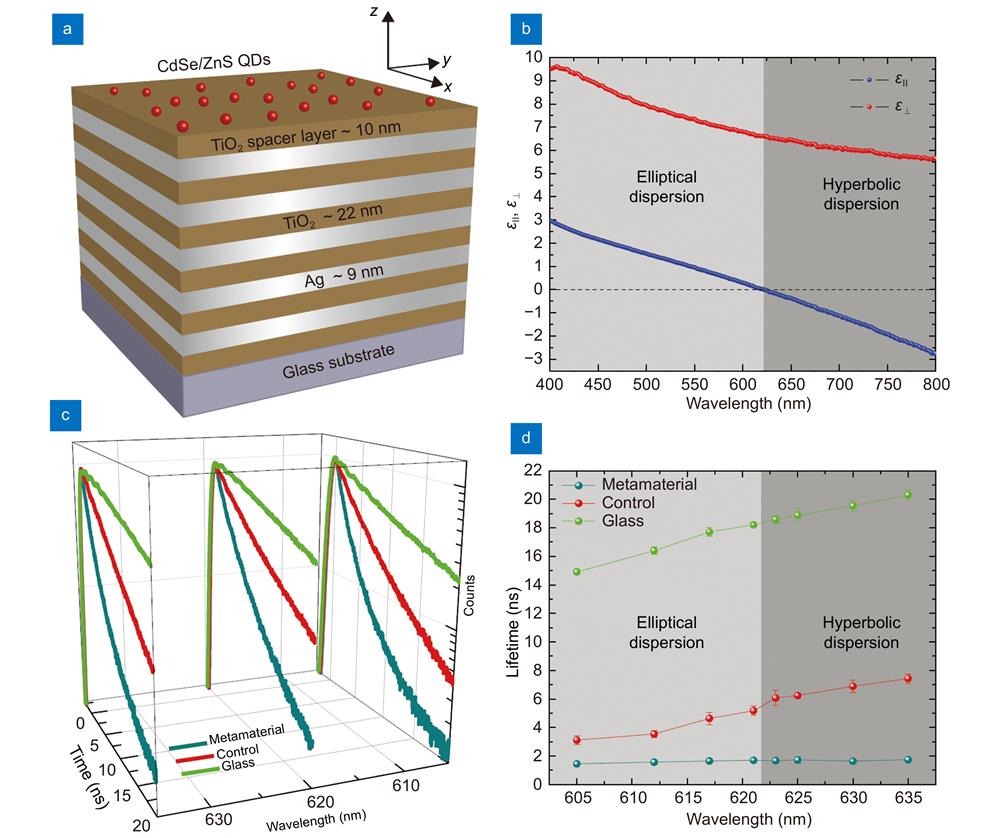
Fig. 2. Photoluminescence enhancement by metal-dielectric multilayer HMMs. (a ) Schematic illustration of Ag-TiO2 multilayer HMM structures. (b ) The real part of effective ordinary and extraordinary permittivities. (c ) Time-resolved photoluminescence from QDs deposited on the HMM, control sample, and glass substrate at 605, 621, and 635 nm. (d ) Lifetime of the QDs as a function of wavelength on the HMM, control sample, and glass substrate. Figure reproduced with permission from ref.54. American Association for the Advancement of Science (AAAS).
Fig. 3. Photoluminescence enhancement by metal-dielectric multilayer HMM cavities. (a ) Schematic illustration of the WS2 monolayer on the HMM cavities. (b ) Type I hyperbolic iso-frequency contour of the HMM. (c ) Scanning transmission electron microscopy (STEM) image of the cross section of a WS2 monolayer on a HMM cavity with chemical composition analysis. (d ,e ) Scanning electron microscopy (SEM) images of HMM cavities with pseudo colors. (f ) Normalized calculated scattering and absorption at cross sections of the HMM cavities with a diameter of 160 nm and a pitch of 380 nm at the bottom. Figure reproduced with permission from ref.90, American Chemical Society.
Fig. 4. Photoluminescence enhancement on trench hyperbolic metasurface. (a ,b ) SEM images of InGaAsP MQW trenches of 100 nm height and 40 nm width, separated by 40 nm trenches. Ag is deposited by sputtering, partially filling the trenches to create a HMS with 80 nm period. (c ) Illustration of optical pumping with different polarizations (TMP‖ or TEP⊥ of the HMS results in collected emission polarized predominantly parallel (TME||) to the metasurface. K
Fig. 5. Plasmonic nanowire-based HMMs. (a ) An array of Au nanorods with approximately 38 nm diameter, 150 nm height and 80 nm spacing embedded in a dye-doped PMMA matrix. (b ) Emission in waveguided modes. Experimental dispersions of the photoluminescence (PL) enhancement measured for TM-polarized emission whose position reproduced from the reflection dispersion is shown as shaded area. Gray dotted line is the light line in air, bulk greyed region is the emission band of LD700 dye. Figure reproduced with permission from: ref.103, American Chemical Society.
Fig. 6. 1D grating out-couplers on multilayer HMMs. Schematic illustration of (a ) Ag slab, (b ) Ag grating, (c ) Ag/Si HMM, and (d ) Ag/Si HMM with grating. R6G fluorescence dye is in PMMA layers. Gratings period is 200 nm.
Fig. 7. 1D and 2D grating out-couplers on multilayer HMMs. (a ) Schematic illustration and (b ) SEM images of HMM with 1D gratings. HMM is composed of four periods of Ag (12 nm thick) and SiO2 (83 nm) layers on top of 100 nm thick Ag substrate as a reflector. The pitch of grating is P = 300 nm. A thin layer of QDs in PMMA is spin-coated on top of the HMM structures. (c ) Schematic of 2D grating in Ag film on HMM with 6 periods of Ag (12 nm) and Al2O3 (23 nm) layers. (d ) SEM image of 2D Ag on top of the PMMA layer with an average period of 500 nm and hole size of 160 nm (top view). (e ) Cross-section view of transmission electron microscope (TEM) image of HMM made of Ag (dark color, 15 nm), Al2O3 (bright color, 15 nm), and embedded QD layer (false color). The bottom and top layers are glass substrate (false yellow) and Pt protection (false violet) layer, respectively (shown in false color). (f ) SEM image of the top view of 2D gratings on HMMs with lattice constant of 255−370 nm with air hole radius of 52−80 nm. Figure reproduced with permission from: (a, b) ref.112, American Chemical Society; (c, d) ref.113, under a Creative Commons Attribution-NonCommercial- ShareAlike 4.0 International License; (e, f) ref.114, PNAS.
Fig. 8. Epsilon-near-zero (ENZ) materials . Sketches of the (a ) single ENZ (MIM) and (b ) double ENZ (MIMIM) structures. A 50 nm thin Al2O3 layer has been deposited on top of each structure as a spacer between the dye (CsPbBr3 nanocrystals) and the Ag layer. (c ) Spontaneous emission and decay times of CsPbBr3 nanocubes deposited on a bare Al2O3 substrate (black), a MIM (red), and a MIMIM (blue) structure 1D grating. (d ) PL enhancement by plasmonic nanostructures. Figure reproduced with permission from ref.135, American Chemical Society.
Fig. 9. Active HMM structure : (a ) dye molecules mixed in PMMA located on top of HMM; (b ) dye molecules arranged in dielectric layers of HMM; (c ) energy diagram of a four-level dye molecule, with an absorption (blue) and emission line (red). Figure reproduced with permission from: (a) ref.148, American Physical Society; (b) ref.149, American Chemical Society.
Fig. 10. FDTD simulations and analytical calculations of emitter-HMM coupling in light reflectance : (a ) reflectance with an absorption line in the weak coupling regime, (b ) strong coupling regime for the finite structure of HMM Fig. 9(b) (logarithmic scale), (c ) real and imaginary parts of the complex eigenfrequencies Ω ± obtained with the model (green curves) in the strong coupling regime. The green and magenta curves are obtained via semi-classical model for two different modes (Eq. (9)). The blue dashed curve is the excitonic absorption line and black dashed curve is the unperturbed optical mode. The two polaritons resulting from the coupling of the optical mode with the excitonic line are identified by numbers 1 and 2 (Ω − and Ω +, respectively). Figure reproduced with permission from ref.149, American Chemical Society.
Fig. 11. Exceptional points (EP) in the system formed by four-level dye molecules embedded in the dielectric medium of multilayer HMMs : (a ) group index in z direction n g ,z of the dye infiltrated multilayer, (b ) zoom on EP1, (c ) zoom on EP3. Orange curves correspond to the band edges at the Brillouin zone center kzD
= 0, magenta curves correspond to the band edges at the Brillouin zone edge kzD
= π, and cyan curves correspond to the gain-loss compensation line where Im(cos(kzD
)) = 0. Figure reproduced with permission from: ref.149, American Chemical Society.
Fig. 12. Coherent interaction between HMM and multiple emitters leading to strong coupling : (a ) schematic diagram of HMM with QDs on top of the polymer spacer, (b ) PL measurement on QD monolayer. The magnitude of the splitting of the various PL peaks are indicated by the quantity ΔE exp. Figure reproduced with permission from ref.109, The Royal Society of Chemistry.
|
Table 1. Summary of photoluminescence enhancement by multilayer HMM structures. Unless noted, emitters are located on the top surface of HMM structures and the works are experimental.
|
Table 2. Summary of photoluminescence enhancement by plasmonic nanowire HMM structures. Unless noted, emitters are located on the top surface of HMM structures and the works are experimental.
|
Table 3. Summary of photoluminescence enhancement by grating out-coupler on HMM structures. Unless noted, emitters are located on the top surface of HMM structures and the works are experimental. Here P is the pitch or lattice constant of the grating out-coupler.


Set citation alerts for the article
Please enter your email address

© Copyright 2018-2021 | Chinese Laser Press. All Rights Reserved 沪ICP备15018463号-20