• Opto-Electronic Advances
  • Vol. 4, Issue 8, 210031-1 (2021)
Leonid Yu. Beliaev1, Osamu Takayama1, Pavel N. Melentiev2、3, and Andrei V. Lavrinenko1、*
Author Affiliations
  • 1DTU Fotonik-Department of Photonics Engineering, Technical University of Denmark, Ørsteds Plads 343, DK-2800 Kgs. Lyngby, Denmark
  • 2Institute of Spectroscopy RAS, Moscow 108840, Russia
  • 3Higher School of Economics, National Research University, Moscow 101000, Russia
  • show less
    DOI: 10.29026/oea.2021.210031 Cite this Article
    Leonid Yu. Beliaev, Osamu Takayama, Pavel N. Melentiev, Andrei V. Lavrinenko. Photoluminescence control by hyperbolic metamaterials and metasurfaces: a review[J]. Opto-Electronic Advances, 2021, 4(8): 210031-1 Copy Citation Text show less

    Abstract

    Photoluminescence including fluorescence plays a great role in a wide variety of applications from biomedical sensing and imaging to optoelectronics. Therefore, the enhancement and control of photoluminescence has immense impact on both fundamental scientific research and aforementioned applications. Among various nanophotonic schemes and nanostructures to enhance the photoluminescence, we focus on a certain type of nanostructures, hyperbolic metamaterials (HMMs). HMMs are highly anisotropic metamaterials, which produce intense localized electric fields. Therefore, HMMs naturally boost photoluminescence from dye molecules, quantum dots, nitrogen-vacancy centers in diamonds, perovskites and transition metal dichalcogenides. We provide an overview of various configurations of HMMs, including metal-dielectric multilayers, trenches, metallic nanowires, and cavity structures fabricated with the use of noble metals, transparent conductive oxides, and refractory metals as plasmonic elements. We also discuss lasing action realized with HMMs.

    Introduction

    Photoluminescence (PL), emission of light from materials, have been widely used for numerous applications ranging from imaging of biological specimen to lasers. Light emitters can take various forms in different material, e.g., fluorescent molecules, quantum dots (QDs), or nitrogen-vacancy centers in diamond1 (NVC). The applications include single molecular detection2, biosensing3-7 and imaging8-10, where a fluorophore as a label is attached to analyte molecules in order to image them or detect their concentration linked with the intensity of emitted fluorescence signals. Detection schemes with fluorescence markers attached to analytes are routinely used in clinical diagnosis. Moreover, for optoelectronic emitting devices it is desirable to enhance their PL emission to improve efficiency of light sources, such as LEDs, lasers, and single-photon sources, since PL is the essential part of their emitting schemes11, 12. This is the main motivation behind many of the recent developments in engineering spontaneous emission using nanoscale structures. Up to present, there have been numerous studies to boost PL by plasmonic, e.g. metal, nanostructures3. For instance, a silver thin film on a glass substrate supports highly localized electric field by mean of a surface plasmon polariton, which strengthens the fluorescence signals of the fluorophores by more than 300%13. Plasmonic nanoantennas tightly focus light within the structure, and thus are routinely used for the enhancement of fluorescent signals2, 14, 15. Interested readers may find review articles on plasmonic nanostructures including plasmonic nanoparticles and gratings for fluorescence enhancement elsewhere16, 17. Another current tendency is to localize fields by Mie-resonances in high-index dielectric nanostructures, such as multilayer stacks18-20, 1D gratings21-27, 2D photonic crystal structures28, as well as, metasurfaces made of dielectric particles29-31.

    In this review, we focus on the enhancement of PL by a class of metamaterials, named hyperbolic metamaterials (HMMs), which are also referred to as an indefinite media, and hyperbolic metasurfaces (HMSs)32-42. Hyperbolic materials are known for the extreme anisotropy and unique dispersion bands in the wavevector space (k-space) generated by the principal permittivity tensor components being of opposite signs. These bands take the shape of a hyperboloid as opposed to spherical or ellipsoid shapes of dispersion contours of dielectric materials. HMMs feature highly localized bulk waves that propagate within the structures which can be used, for example, for sensing43-45, sub-diffraction imaging46, and directional emission of light by quantum emitters47, 48. The underlying features used for the control of PL by HMMs are large accepted wavevectors (high-k case), highly localized fields and large optical density of states, leading to enhanced light-matter interactions (increase in the Purcell factor) and control of emission directivity49, 50. High-k modes wavevectors values of HMM can reach infinity for semi-infinitely thick HMMs although in reality the numbers are limited by finite thickness of HMM slabs51 and inapplicability of effective media approximation to HMMs52, 53. Apart from high-k modes supported by HMMs, they offer the following three unique features indispensable for PL enhancement and control:

    A. Broadband hyperbolic region.

    B. Tunability of hyperbolic region.

    C. Directionality by highly anisotropic nature of HMM.

    Regarding (A) point above, the hyperbolic region is extremely broad and extends from certain cut-off wavelength and beyond, starting from visible wavelengths to near-infrared54 or even to mid-infrared wavelengths55, which contrasts with dielectric structures with Mie resonances and plasmonic nanostructures whose resonance is usually confined to certain band of wavelengths. This is the unique feature and clear advantage of HMMs in order to enhance whole emission bandwidth of emitters. The cut-off wavelength of HMM as is stated in the listed advantage (B) can be tailored for desired wavelength regions by the design of HMMs, such as choice of materials, more specifically the permittivity of metal and dielectric elements and their volume fraction. Regarding the feature (C), the directionality of emission on HMM can also be exploited to create directional emitter in-plane47, 48 and out of plane of HMM surfaces56. These (A) to (C) features are combined to make HMMs an attractive platform for enhancement and control of PL.

    Apart from the underlined unique nature of HMMs, we discuss the control of PL in terms of (1) intensity enhancement, (2) lifetime reduction, (3) spectral region, (4) directivity, and (5) lasing. Different configurations of HMMs have been studied for the enhancement of photoluminescence from fluorescence dyes, quantum dots, perovskites and nitrogen-vacancy centers in diamond. In order to describe these features, this review is organized as in the following. We start with introduction of hyperbolic metamaterials and describe their dispersion in wavevector space, which can be categorized as type I and II hyperbolic regions or HMMs. We also overview each type of HMM structures, such as metal-dielectric multilayers, trenches which is the vertical version of metal-dielectric multilayers, and nanowires. These are the basic building blocks of HMMs. Out-coupling of enhanced PL emission from metal-dielectric multilayer type HMM is difficult since emitted light is trapped within HMM. Therefore, often, grating out-couplers are integrated into HMM structures and we cover various types of grating out-couplers built on HMMs. As a special case of HMMs, we show PL enhancement by epsilon-near-zero (ENZ) materials. Finally, we discuss the active HMMs with gain media to compensate the absorptive loss of the structures. Throughout the article, we confine ourselves to the light wavelengths ranging from UV to near-infrared, λ = 290 – 1000 nm.

    Hyperbolic metamaterials

    In the case of uniaxial anisotropic medium, a relative permittivity tensor [ε] is expressed by

    $\left[ {\epsilon } \right] = \left( {\begin{array}{*{20}{c}} {{{\epsilon }_x}}&0&0\\ 0&{{{\epsilon }_y}}&0\\ 0&0&{{{\epsilon }_z}} \end{array}} \right),$ (1)

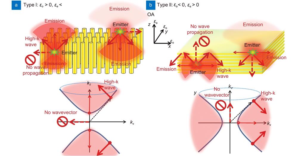
    where εx = εy = εo, and εz = εe, εo and εe are ordinary and extraordinary permittivities, respectively. When εo = εe > 0, the medium is an isotropic dielectric, while when εo = εe < 0 – it is an isotropic plasmonic material, for example metal. A HMM or hyperbolic material is a medium when the permittivity components along the principle axes have opposite signs, namely εoεe < 0, and the iso-frequency surface of extraordinary waves given by equation

    $({k_x}^2 + {k_y}^2)/{{\epsilon }_{\rm{o}}} + {k_z}^2/{{\epsilon }_{\rm{e}}} = {\omega ^2}/{c^2}\;,$ (2)

    becomes a hyperboloid, where kx, ky, kz are the wavevector components, ω is the angular frequency and c is the speed of light in vacuum. There are two types of hyperboloid as shown in Fig. 1, which are conventionally classified as: 1) type I HMM: εo > 0 and εe < 0, and 2) type II HMM: εo < 0 and εe > 0.

    Schematic illustration of hyperbolic metamaterials and metasurfaces. (a) Type I hyperbolic metamaterials (εo > 0 and εe b) Type II hyperbolic metamaterials (εo εe > 0) in metal-dielectric multilayer configuration and their dispersion in the wavevector space.

    Figure 1.Schematic illustration of hyperbolic metamaterials and metasurfaces. (a) Type I hyperbolic metamaterials (εo > 0 and εe < 0) in metallic nanorod or nanowire configuration and their representative dispersion in the wavevector space (k-space). ( b) Type II hyperbolic metamaterials (εo < 0 and εe > 0) in metal-dielectric multilayer configuration and their dispersion in the wavevector space.

    In the case of type I HMM, the dispersion band forms a two-fold hyperboloid in the wavevector space (k-space)42, as illustrated in Fig 1. Typically, a type I HMM can be realized by a metallic nanowire structure43, 57, while type II HMM - by a metal-dielectric multilayer stack with deeply subwavelength layers44, 58, 59. Note that in the case of most of naturally occurring materials, both ordinary (εo) and extraordinary (εe) permittivity components are of the same sign, resulting in either spherical (εo = εe, isotropic materials) or elliptical iso-frequency surfaces when εoεe. However, there are some natural materials that exhibit hyperbolic dispersion for certain wavelength ranges35, 36.

    Materials with hyperbolic iso-frequency contours support propagation of lightwaves with large wavevectors (high-k waves) and correspondingly short effective wavelengths. However, for certain directions in the k-space, there are no any wavevectors available, and, therefore, propagation of light in such direction is prohibited. The high-k lightwaves within HMMs are called bulk plasmon polaritons, BPPs (sometimes also called as volume plasmon-polaritons), as well as hyperbolic surface waves (sometimes referred to as Dyakonov plasmons) that are supported on the top surface of HMMs47, 48, 60. BPPs propagate and are tightly confined within HMM structures55, 57, 61. Such high-k waves in metal-dielectric multilayer systems are known to originate from the hybridization of short-ranged surface plasmon polaritons supported in each of the dielectric-metal-dielectric set61, 62. Usually, BPPs exhibit highly localized intense electric fields, which together with a non-resonant (broadband) spectral range of their existence, makes them rather convenient tools for the enhancement of PL. A single emitter as a source of PL can be considered as a point dipole that emits light in the form of both propagating (far-field) and evanescent (near-field) waves. In free space, emitted light transfers into far-field propagating waves, and the emitter relaxes by losing energy. However, in the vicinity of a HMM, the near-field components of emitted light are more efficiently coupled to the evanescent (near-field) components of BPPs with wavenumbers higher than those of the far-field propagating waves, creating a new decay mechanism for the emitter, since the emitted energy is directly sucked by the BPP modes. This results in the reduced lifetime of emitters in comparison with the free space situation. A typically large number of BPP modes supported by HMMs produces an increased photonic density of states (PDOS), leading to a broadband enhancement of the spontaneous emission, referred to as Purcell’s effect49, 50, 63, 64. In order to characterize the PL enhancement, either the PL intensity or the emission life time (or both) measurement as opposed to the reference emitter samples on a glass substrate or on metal films are typically employed.

    Metal-dielectric multilayers

    Metal-dielectric multilayer HMMs have been studied and realized extensively due to the relative ease of fabrication. Their layer thicknesses should be sufficiently smaller than the wavelength of light that they can be characterized by effective parameters, i.e. effective permittivity tensor. By design of a metamaterial (i.e. choosing materials, thicknesses of each layer, filling fraction), the effective dielectric functions or permittivities can be tuned to hyperbolic iso-frequency surface in the wavelength region of interest (see Fig. 1). So, to characterize the optical properties of a HMM, the first step is to find its effective permittivities, and the simplest approach is based on the effective medium approximation (EMA)38, 65, 66. In the case of metal-dielectric multilayers, the effective ordinary and extraordinary permittivities, εo, εe are expressed by

    ${{\epsilon }_{\rm{o}}} = {f_{\rm{m}}}\cdot{{\epsilon }_{\rm{m}}} + {f_{\rm{d}}}\cdot{{\epsilon }_{\rm{d}}},$ (3)

    ${{\epsilon }}_{{\rm{e}}}=({{\epsilon }}_{{\rm{m}}}\cdot {{\epsilon }}_{{\rm{d}}})/({f}_{{\rm{d}}}\cdot {{\epsilon }}_{{\rm{m}}}+{f}_{{\rm{m}}}\cdot {{\epsilon }}_{{\rm{d}}}){,} $ (4)

    where εm, εd, fm, and fd are the permittivities of the metal and dielectric, and filling factors of metal, and dielectric layers in the multilayer structure, respectively. The light emitters placed into the near-field of optical modes supported by HMMs release their energy predominantly via radiative emission and excitation of plasmonic modes and other non-radiative channels, where usually plasmonic modes dominate as the decay channel.

    The first experimental evidence of fluorescence enhancement was demonstrated on a multilayer HMM that consist of 16 stacked layers of gold (Au, 19 nm) and alumina (Al2O3, 19 nm) with a 21-nm thick epoxy with dispersed rhodamine 800 (Rh800)67, where 1.8-fold reduction of the lifetime was reported. The control of spontaneous emission with multilayer HMMs with alternating metal and dielectric layers was described in ref.68. Several different samples were fabricated for the sake of comparison, such as Ag(25 nm, 11 layers)/PMMA(30 nm, 10 layers), Ag(30 nm, 5 layers)/LiF(40 nm, 4 layers), Ag(30 nm)/LiF(40 nm) with 8 periods, Ag(20 nm)/MgF2(30 nm) with 8 periods. Two types of dyes were exploited for PL study: IR-140 dye, whose emission peak lies at λ ≈ 850 nm, as well as rhodamine G6 (R6G). Compared with the reference glass substrate, shortening of the luminescence life-times was observed for all samples. For the Ag/MgF2, the best result was 1.4-times shortening, for Ag/LiF - 1.5-times, and for Ag/PMMA - 5.7-times.

    Apart from Ag layers, Au has been extensively used as the constituent of multilayer HMM structures. HMMs that consist of 16 stacked layers of gold (Au) and alumina (Al2O3) on a glass substrate with a 21-nm dye thin film of epoxy mixed with rhodamine 800 (Rh800) at a 100 µM concentration spin coated on top of the spacer layer were realized for fluorescence enhancement69. For comparison purposes, two control samples with single thick (300 nm) and thin (20 nm) gold layers were also fabricated. In addition, a reference dye thin film was prepared on a bare glass substrate. The dye concentration in the thin film affects the dye parameters. At high concentrations, above 100 M, the fluorescence lifetime in dye-epoxy solution is rapidly reduced due to quenching processes, while at low concentrations the fluorescence lifetime is independent of concentration. In thin films of rhodamine 800 embedded in an epoxy matrix, the quantum yield of the dye gradually increases with decreasing concentration. In the experiments, a 100 µM concentration was chosen to avoid concentration quenching and to obtain better performance with a higher quantum yield. The PL signal for the 89-nm spacer layer is about 9.3 times stronger for both the HMM and the thick gold substrates (compared with the bare glass substrate), while the thin gold film provides about 6.4 times enhancement.

    Enhancement of photoluminescence from colloidal core-shell QDs of cadmium selenide and zinc sulfide (CdSe/ZnS) in proximity with a multilayer HMM was demonstrated54. Quantum dots were placed on top of the structure, consisting of alternating layers of silver (Ag, 9 nm thick) and titanium dioxide (TiO2, 22 nm) as shown in Fig. 2. Time-resolved PL measurements were carried out on the metamaterial sample, the control sample, and the glass substrate (Fig. 2(c, d)) at the anticipated transition wavelength (elliptic-to-hyperbolic regime, at 621 nm) and on both sides from it (605 and 635 nm). When compared with the control sample, the metamaterial enhanced the spontaneous emission rate by a factor of 3 at the transition wavelength and by a factor of 4.3 deeper in the hyperbolic regime (635 nm). The overall reduction in the lifetime of the QDs when compared with those on a glass substrate is 11 ns. The lifetime of the QDs increases as a function of wavelength on both the glass substrate and the control sample [Fig. 2(d)]. This is due to the size distribution of QDs and the dependence of the oscillator strength on energy. The metamaterial sample exhibits a decrease in the lifetime as a function of wavelength in the hyperbolic regime, while such variation is very small in the elliptical spectral region. The lifetimes of QDs on both structures with 1 and 10 bilayers are almost the same in the elliptical spectral region, but significantly differ above the critical wavelength. The large change in the spontaneous emission lifetime of the QDs on the metamaterial compared with the glass substrate and 1 bilayer case is explained by excitation of the high-k BPPs in the metamaterial, as well as by the nonradiative contribution of the surface plasmon polariton (SPP) modes at the metamaterial interface.

    Photoluminescence enhancement by metal-dielectric multilayer HMMs. (a) Schematic illustration of Ag-TiO2 multilayer HMM structures. (b) The real part of effective ordinary and extraordinary permittivities. (c) Time-resolved photoluminescence from QDs deposited on the HMM, control sample, and glass substrate at 605, 621, and 635 nm. (d) Lifetime of the QDs as a function of wavelength on the HMM, control sample, and glass substrate. Figure reproduced with permission from ref.54. American Association for the Advancement of Science (AAAS).

    Figure 2.Photoluminescence enhancement by metal-dielectric multilayer HMMs. (a) Schematic illustration of Ag-TiO2 multilayer HMM structures. (b) The real part of effective ordinary and extraordinary permittivities. (c) Time-resolved photoluminescence from QDs deposited on the HMM, control sample, and glass substrate at 605, 621, and 635 nm. (d) Lifetime of the QDs as a function of wavelength on the HMM, control sample, and glass substrate. Figure reproduced with permission from ref.54. American Association for the Advancement of Science (AAAS).

    Directional PL enhancement of dyes on multilayer HMMs was studied for the sample consisting of 20 alternating layers (10 periods) of Au (15 nm thick) and Al2O3 (28 nm thick)70. A dye-dissolved PMMA layer was deposited on top of the HMM, separated by an Al2O3 spacer layer of thickness 12 nm from the HMM interface. Coumarin 500 was selected as the organic dye that emit light at wavelength 480 nm. The structure showed a 2-fold enhancement of spontaneous emission during time-resolved photoluminescence measurements. A similar experiment was conducted on Au-Al2O3 multilayer HMMs with 19 nm thick metal and dielectric layers, where 3 times reduction in emission lifetime of nitrogen vacancy centers (NVCs) in nanodiamonds was demonstrated71. The enhancement of single–photon emission from NVCs in nanodiamonds was also observed for a planar multilayer metamaterial that consisted of CMOS-compatible ceramics: titanium nitride (TiN) and aluminum scandium nitride (AlxSc1-xN)72. Such structure improved the emission properties of a single NVC nanodiamond placed on top. Lifetime reduction was from 17 ns on a reference sample to 4.3 ns on the HMM on average. The Purcell factor corresponded to the value 4. Moreover, it was found that the collected emission power for NVCs near the HMM was increased by a factor of 1.8 on average, although a quite remarkable enhancement of 4.7 was detected in one particular case. A TiN-based multilayer HMM with 10 alternating layers (5 periods) of TiN and SiO2 deposited on a glass substrate was used for the enhancement of QD emission73. A 20 nm thick Si QDs layer was deposited on the top of the HMM and up to 1.6-times enhanced emission decay rate was observed in respect with identical QDs deposited on silica glass. Up to the 4.4-fold fluorescence enhancement from the nanocomposites made of CdTe QDs monolayers placed between layers of gold nanoparticles was demonstrated74. Later on, it was theoretically demonstrated that such structures represents itself a hyperbolic metamaterial and thus is able of increasing the radiative decay rate of emission centers placed inside the structures75. Depending on the geometric parameters, such as thickness of the spacer layer, the number of quantum dots and nanoparticle layers, effective permittivity tensor of the entire nanocomposite may become indefinite or hyperbolic. This fact leads to the rise in the photonic density of states, in turn resulting in strong enhancement and pronounced polarization anisotropy of QDs luminescence. Enhancement of UV emission from semiconductor nanoparticles76 and multiple quantum wells (MQWs)77, 78 deposited on HMMs was also demonstrated.

    Upper-excited state emission from molecules is not usually observed owing to strong competition with much faster nonradiative relaxation pathways. However, the radiative decay rate can be increased by modifying the PDOS. Zinc tetraphenylporphyrin (ZnTPP) molecules as emitters embedded in a HMM were shown to enable a 18-fold increase in fluorescence intensity from the second singlet excited state relative to that from the lowest singlet excited state79. Varying the number of periods of the HMM stack enables systematical tuning of the ZnTPP fluorescence spectrum from red (dominated by emission from lowest singlet excited state) to blue (dominated by emission from the second singlet excited state).

    Spin-coated organic thin films based on the quinoidal oligothiophene derivative (QQT(CN)4) were demonstrated to exhibit hyperbolic dispersion over a wide spectral range from 670 to 920 nm80. To study the influence of QQT(CN)4 dispersion on the Styryl 9M light-emitting dye molecules, blend films containing a polyvinylpyrrolidone (PVP) host doped with dye molecules were deposited on top of three different substrates: (1) fused silica (FS), (2) 80 nm thick dielectric-metal HMMs containing 4 Ag/Al2O3 pairs and (3) organic monolithic natural hyperbolic materials based on a 60 nm thick QQT(CN)4 film. To gain further insights, polyvinyl alcohol (PVA) layers (spin-coated from water) with thicknesses of 25 and 100 nm were also inserted between the three types of substrates and the PVP blends. The photoluminescence exhibited slower dynamics at longer wavelengths. The fluorescence decays were described by the sum of two exponential functions. The presence of the two fluorescence lifetimes were attributed to the presence of Styryl 9M monomers and higher aggregates in the PVP blends. The Purcell factor was measured to be around 1.3 and 1.4 on top of the QQT(CN)4 and HMM substrates correspondingly.

    It is well-known that the effective medium theory applied for characterization of dielectric multilayer system and HMMs can experience a breakdown, depending on the thickness of each layer, number of periods, etc.53, 81. Recently the optimum number of periods of a multilayer HMM for the enhancement of PL from a quantum emitter was theoretically analyzed82. In practical system, the number of periods is finite and it is essential to design a multilayer HMM with the optimum number of periods to enhance PL by achieving the highest PDOS. In this work, HMMs consisting of 3, 5, and 8 periods of Au (15 nm)/SiO2 (25 nm) pairs with a quantum emitter, placed inside and in near vicinity of the HMM surface were studied. Modeling confirmed that multilayer HMM slabs with lower number of periods, 3 periods in this study, provide higher total PDOS, giving rise to larger transition rate enhancement. The unit cell thickness can also affect enhancement of quantum dots emission83. The total thickness of Ag/ITO HMMs was kept 320 nm, while the unit cell thickness ranges from 20 to 80 nm. The study suggested that the Purcell factor increases as the unit cell thickness decreases, exhibiting the maximum enhancement factor of about 40. Related analysis was done in work84, where the number of layers and their thickness were varied to study changes of the Purcell factor. The HMM was composed of alternate silver and silicon layers with a dipolar emitter on top of it. It was shown that the multilayer structures with a few layers of small thickness outperform those with many layers of large thickness in terms of the Purcell effect. Such effect was attributed to the larger wavevectors and localization of modes due to the stronger coupling between short range SPPs on thinner metal layers.

    Unlike conventional planar multilayer HMMs, HMMs with a curved surface demonstrated an efficient out-coupling of nonradiative modes due to the gradual tapering of HMMs thickness down to few nm. Such outcoupling leads to enhanced spontaneous emission85. High-k plasmonic modes propagate along the curved surfaces are then outcoupled into radiative modes and emitted into the far field, realizing a directional light emission with the maximal fluorescent intensity. Detailed simulations revealed a high Purcell factor and a spatial power distribution in the curved HMM, which agreed with the experimental result. The HMMs consist of 20 stacked layers (10 periods) of Ag and TiO2 deposited on top of a tapered glass capillary. On top of the uppermost Ag layer, an extra 10-nm-thick TiO2 spacer was deposited to decrease the dye absorption. The fabricated HMM has a gradient in its thickness due to the directional deposition. Subsequently, the HMM-capped tapered glass capillary was dipped into the solution of R6G with a concentration of 100 µM. The PL-intensity distribution indicates enhancement of both its directionality and efficiency. Such curved HMMs, maintaining excellent property in the Purcell effect, can achieve an 80-fold maximum intensity enhancement for directional emission compared with planar HMMs. Another flexible HMM that can be folded was realized by Au and polymer (PVA) layers, with water-soluble characteristics86. These transient HMMs devices can be easily washed away, disappearing with just few drops of deionized water at room temperature. Two samples were made with different fill-fractions of Au: 37.31% (marked as the HMM1) and 26.87% (marked as the HMM2), and various dye molecules embedded inside PMMA. The photoluminescence kinetics was measured to explore the spontaneous emission effect. The best enhancement of 5.55 (3.80) times for the HMM1 (HMM2) was achieved for the R6G dye molecules.

    In order to enhance emission to far-field, metallic cylinder patch antennas can be integrated with HMM structures87, 88. As an example, a 5-layered planar HMM structure consisting of Au and zinc sulfide (ZnS) layers with a cylindrical Au patch antenna on the top was modeled87. Silicon carbide (SiC)-based emitters with emission peaks around 900 nm were placed inside the HMM. For dipole orientation perpendicular to the interface, the HMM-coupled antenna leads to a spontaneous emission enhancement with a Purcell factor on the order of 400 at 850 nm and 300 at 680 nm. A similar order of enhancement was actually reported throughout the broad spectral range of 650−1000 nm. Similarly, a cylindrical Ag patch antenna on top of HMM structures with 5, 9, 13, and 17 periods of Ag (24 nm) and TiO2 (30 nm) layers was optimized for dipole emission at 660 nm88. After characterization, the best 200-fold emission enhancement of CdSeS/ZnS core-shell QDs embedded inside the HMM was achieved for the 5-layered structure. This tendency of better enhancement by fewer periods of HMMs confirms conclusions stemmed from the theoretical analysis82.

    Optical cavities or resonators made of dielectric materials can trap photons and support strong electric fields, however, the smallest size of such cavities is limited to the order of effective wavelengths of light, λ/n, where n is the refractive index of the dielectric. In case of HMMs with high-k (large mode refractive index) BPPs, the effective wavelength can be small and hence the size of cavities made of HMMs can be deeply subwavelength, much smaller than conventional dielectric cavities. Such confinement leads to smaller mode volumes and, hence, more intense electric fields in the nanocavities, resulting in the enhancement of the emission rate. An HMM nanocavity was initially demonstrated for 2 to 4 periods multilayers HMMs curved into pyramid shape89. Recently, HMM resonators were used for the enhancement of emission from a transition metal dichalcogenide (TMDC) monolayers, WS2, in order to boost light-matter interactions with an atomically thin TMDC film as illustrated in Fig. 390. The authors demonstrated about 30-fold enhancement of the overall photoluminescence emission intensity from a WS2 monolayer that is placed on top of the HMM resonators. Remarkably, the structure enhances both the excitation (absorption) at 514 nm and radiative decay rate at 620 nm.

    Photoluminescence enhancement by metal-dielectric multilayer HMM cavities. (a) Schematic illustration of the WS2 monolayer on the HMM cavities. (b) Type I hyperbolic iso-frequency contour of the HMM. (c) Scanning transmission electron microscopy (STEM) image of the cross section of a WS2 monolayer on a HMM cavity with chemical composition analysis. (d,e) Scanning electron microscopy (SEM) images of HMM cavities with pseudo colors. (f) Normalized calculated scattering and absorption at cross sections of the HMM cavities with a diameter of 160 nm and a pitch of 380 nm at the bottom. Figure reproduced with permission from ref.90, American Chemical Society.

    Figure 3.Photoluminescence enhancement by metal-dielectric multilayer HMM cavities. (a) Schematic illustration of the WS2 monolayer on the HMM cavities. (b) Type I hyperbolic iso-frequency contour of the HMM. (c) Scanning transmission electron microscopy (STEM) image of the cross section of a WS2 monolayer on a HMM cavity with chemical composition analysis. (d,e) Scanning electron microscopy (SEM) images of HMM cavities with pseudo colors. (f) Normalized calculated scattering and absorption at cross sections of the HMM cavities with a diameter of 160 nm and a pitch of 380 nm at the bottom. Figure reproduced with permission from ref.90, American Chemical Society.

    Förster resonance energy transfer (FRET) is the nonradiative transfer of excited state energy from one fluorophore (donor) to another fluorophore (acceptor) via a dipole−dipole coupling process91, 92. FRET for donor-acceptor pairs located on top of a HMM was experimentally studied for the environments with high local densities of photonic states93. Authors observed strong collective interactions of the dye molecules and surface plasmon polaritons, which can affect the absorption and emission spectra and, correspondingly, influence the rate of the Förster energy transfer.

    Apart from fluorescence dye, quantum dots, and NVCs, nanocrystals of lead halide perovskite, namely CsPbI3, were used as emitters placed on top of HMMs to study the enhancement of the Purcell factor94. The multilayer HMM contained 6 or 8 periods of Ag (25 nm or 40 nm) and LiF (35 nm or 40 nm) with CsPbI3 placed on a 10−50 nm thick spacer on top of the HMMs. CsPbI3 nanocrystals with size distribution of 11−16 nm emits light at around 520 nm when excited by 405 nm laser radiation, 3-fold reduction of emission lifetime was observed when the nanocrystals were placed on top of the HMMs. Interestingly, very similar enhancement of radiative rate recombination, by almost 3 times, in quasi-2D perovskite thin films of BA2Cs3MA3Pb7Br2I20 composition deposited on top of gold-alumina HMMs of different thicknesses (from 2 to 7 periods) was reported95. The Purcell factor was demonstrated to grow almost linearly with the number of periods in contrary to ref.75, 81. It means that it is necessary to take into account properties of active material since it has significant influence on spontaneous emission process. The Purcell factor also depends on the pump power. For the pump intensity about 0.2 pJ, there are no any difference in the rate enhancement produced by 2- and 7-period HMMs. However, with the increase in pumping to 20 pJ, there is a significant difference in the Purcell factor: 1.62 versus 3.1.

    Most of multilayer HMMs are fabricated on a rigid planar substrate which cannot be bent. However, recently multilayer HMMs on flexible rollable paper substrate have been demonstrated96. The fabricated structures consisted of four periods of Au(25 nm) and PMMA polymer (30 or 40 nm) multilayers deposited on a flexible PDMS intermediate layer and rollable paper substrate. The structures can be rolled up to the curvature radius of 1 mm without performance degradation. The emitter is an organic–inorganic perovskite nanocrystal, CH3NH3PBr3, which emits light in the visible wavelengths of 520−550 nm. In the paper, 3.5 times enhancement of emission intensity was reported. This new type of HMMs was used to demonstrate enhancement of stimulated emission, as well as laser action.

    Emission of quantum dots can be strongly enhanced via coupling to aperiodic metal-dielectric multilayers. Two such cases are reported in literature97, 98. In both cases, colloidal CdSe/ZnS quantum dots were placed on top of aperiodic sequences of metal and dielectric thin films. The decay rate of quantum emitters was characterized by standard lifetime measurements of fluorescence. For comparison characterization was also conducted with HMM structures composed of Ag and SiO2 layers with the same metal filling ratio as in the aperiodic stack and thicknesses of 20 nm each. The sample with aperiodic structure was based on the use of Fibonacci sequence (FS)97. The fluorescence decay curves showed a biexponential behavior. The contribution of the faster decay components was dependent on the density of QDs, and it was minimized by reducing their concentration. First, the lifetime of quantum dots near the uniform silver film and HMM samples was checked giving shorter life time for the latter case. This result indicates that the reduction of lifetime for the HMM is not simply the extinction effect (quenching) due to presence of silver, but regards to the presence of high-k modes. Next, the lifetime on the HMM and FS samples was compared, showing stronger reduction of lifetime by the FS sample. This comparison indicates that the combined contribution of larger PDOS for FS is higher than that of the HMM. The experimental results were consistent with simulations showing a 1.35 fold Purcell factor enhancement on the Fibonacci sequence multilayer than on the HMM and 260-nm-thick silver film (control sample) on one particular wavelength.

    Another periodic multilayer arranged in a Tue-Morse (TM) sequence (8 layers ABBABAAB, where A and B represent Au and SiO2 layers with thicknesses of 20 and 80 nm, respectively) was compared with a periodic HMM (4 periods, 8 layers) with the same filling fraction98. The photoluminescence measurements were performed for the QDs on the two multilayer stacks and the glass substrate at the emission wavelength of 580 nm. The most substantial reduction occurred on the wavelength 640 nm with quantified lifetime reduction in 1.45 and 1.33 times for TM multilayer stacks and periodic HMMs respectively.

    The summary of the following chapter is presented in Table 1. From the table, one can see materials used for both metal and dielectric layers, emitters, and enhancement factors. The metallic layers are mostly made of either Ag or Au and a wide variety of materials are used for the dielectric layers, such as silica (SiO2), alumina (Al2O3), titania (TiO2), polymers. The number of periods is in the range of 4 to 10. From the data presented in the table it follows that depending on the structure the fluorescence can be enhance from 1.3 to 200-fold.

    HMM structures and materialsEmitters (emission peak wavelength)Enhancement factorReferences (year)
    Au(19 nm)/Al2O3(19 nm), 8 periods Rhodamine 800 (715 nm)1.8-fold reduction of lifetimeref.67 (2010)
    Ag(25 nm, 11 layers)/PMMA(30 nm, 10 layers); Ag(30 nm, 5 layers)/LiF(40 nm, 4 layers); Ag(30 nm)/LiF(40 nm) 8 periods, and Ag(20 nm)/MgF2(30 nm) 8 periods IR-140 dye (850 nm)1.4 for Ag/LiF; 5.7 for Ag/PMMAref.68 (2011)
    Au(19 nm)/Al2O3(19 nm), 8 periods Rhodamine 800 (720 nm)9.3ref.69 (2012)
    Ag(9 nm)/TiO2(22 nm), 10 periods CdSe/ZnS colloidal QDs (630 nm)3ref.54 (2012)
    Au(15 nm)/Al2O3(28 nm), 10 periods Coumarin 500 (480 nm)2ref.70 (2013)
    Au(19 nm)/Al2O3(19 nm), 8 periods NVC (637 nm)2.57ref.71 (2013)
    Au nanoparticles (15 nm)/CdTe QDs (5.5 nm), separated by dielectric (PDDA/PPS) spacers with varied thickness (0–10 nm), 2–5 periodsCdTe QDs (590 nm)4.4ref.74, 75 (2011, 2014)
    TiN(8.5 nm)/Al0.7Sc0.3N(6.3 nm),10 periods NVC (600–800 nm)4.7 max Purcell factorref.72 (2015)
    TiN(15 nm)/SiO2(15 nm), 5 periods 20 nm thick Si QDs (720 nm)1.6ref.73 (2015)
    Ag(25 nm) 7 layers /MgF2(35 nm) 6 layers HITC dye-doped polymeric film (860 nm) 7ref.78 (2015)
    Ag(10 nm)/TiO2(30 nm), 10 periods Rhodamine 6G (R6G, 540–600 nm)80-fold intensity enhancementref.85 (2018)
    Au(26.87–37.31%)/poly(vinyl alcohol) (PVA), 4 periodsR6G dye (540–600 nm)1.55 for HMM1, 1.18 for HMM2ref.86 (2018)
    Ag(22 nm)/MoO3(10 nm) 6 periods, HMM; Ag(12 nm)/MoO3(20 nm) 6 periods, elliptic ZnO nanoparticles (395 nm)Lasing threshold 20% less and 6 times emission intensityref.76 (2018)
    Al(20 nm)/MgF2(20 nm), 4 periods 15-nm thick AlGaN MQWs (318 nm)160-fold emission rateref.77 (2018)
    Au(30 nm)/ZnS(30 nm) 5 periods, with cylindrical gold patch antennaSiC (900 nm)Purcell factor of 400 at 850 nm. (Theory)ref.87 (2018)
    Ag(25 nm)/PMMA(30 nm), 5 periodsZinc tetraphenylporphyrin (ZnTPP), S1 (580–670 nm), S2 (400–460 nm) 18-fold increase in fluorescence intensity from S2 state to S1. ref.79 (2018)
    320 nm thick HMM of Ag/ITO with unit cell thickness from 20 to 80 nmCdSe/ZnS QDs (550 nm)40-fold intensity enhancementref.83 (2018)
    Quinoidal oligothiophene derivative QQT(CN)4 (60 nm thick), 670 to 920 nm Styryl9M dye (680–850 nm)1.3-1.4 Purcell factorref.80 (2019)
    Ag(24 nm)/TiO2(30 nm) 5, 9, 13, and 17 layers with cylindrical Ag antenna CdSeS/ZnS QDs (660 nm)200-fold enhancement for 5-layered HMMref.88 (2020)
    Au(15 nm)/SiO2(25 nm) 3, 5, and 8 periods Emitter (600–1600 nm)60–85 (Theory)ref.82 (2020)
    Ag(16 nm)/Al2O3(24 nm), 3 periods WS2 monolayer (615 nm) 30-fold enhancement of the overall PL intensityref.90 (2020)
    Ag(25 nm)/LiF(35 nm) and Ag(40 nm)/LiF(40 nm), 6 or 8 periodsCsPbI3 Perovskite nanocrystals (520 nm) 3-fold Purcell enhancementref.94 (2020)
    Au(10 nm)/ Al2O3(10 nm), 2–7 periods BA2Cs3MA3Pb7Br2I20 Perovskite film (700 nm) 1.6-3-fold Purcell enhancement depending on number of periodsref.95(2021)
    Ag(25 nm)/PMMA(40 nm) and Ag(25 nm)/PMMA(30 nm), 4 periods on paperMAPbBr3 perovskite nanocrystals (520–550 nm) 3.5-fold intensity enhancementref.96 (2021)
    Aperiodic Ag (20 nm, 6 layers)/SiO2(20 nm, 6 layers) in Fibonacci sequence Colloidal CdSe/ZnS QDs (640 nm)1.6 than Ag layer, 1.35 than periodic materialref.97 (2014)
    Aperiodic Ag(20 nm, 8 layers)/SiO2(80 nm, 8 layers) in Tue-Morse (TM) sequence Colloidal CdSe/ZnS QDs (640 nm)1.45 than glass substrateref.98 (2019)

    Table 1. Summary of photoluminescence enhancement by multilayer HMM structures. Unless noted, emitters are located on the top surface of HMM structures and the works are experimental.

    Plasmonic trench structures

    Apart from a conventional configuration of horizontal metal and dielectric layers, a HMM can be realized with vertically standing layers (Fig. 4). Such deep subwavelength plasmonic gratings can be characterized as hyperbolic metasurfaces (HMS)99 or so-called trench structures (HMMs)55, 100. The HMS exhibits in-plane anisotropy, which leads to hyperbolic dispersion and supports both directional surface waves and bulk plasmon modes propagating inside of the trenches. An emitter placed on the surface will show emission in specific directions only47, 48. Ag-based trenches with semiconductor InGaAsP quantum walls as emitters embedded in the trenches were realized as the HMS as shown in Fig. 456. The trench HMS displayed extreme absorption and emission polarization anisotropy. Hyperbolic dispersion was verified by finite difference time domain (FDTD) simulations and > 350% emission intensity enhancement was experimentally observed relative to the bare semiconductor quantum wells.

    Photoluminescence enhancement on trench hyperbolic metasurface. (a,b) SEM images of InGaAsP MQW trenches of 100 nm height and 40 nm width, separated by 40 nm trenches. Ag is deposited by sputtering, partially filling the trenches to create a HMS with 80 nm period. (c) Illustration of optical pumping with different polarizations (TMP‖ or TEP⊥ of the HMS results in collected emission polarized predominantly parallel (TME||) to the metasurface. KB is the Bloch wavevector. Figure reproduced from ref.56, under a Creative Commons Attribution 4.0 International License.

    Figure 4.Photoluminescence enhancement on trench hyperbolic metasurface. (a,b) SEM images of InGaAsP MQW trenches of 100 nm height and 40 nm width, separated by 40 nm trenches. Ag is deposited by sputtering, partially filling the trenches to create a HMS with 80 nm period. (c) Illustration of optical pumping with different polarizations (TMP or TEP of the HMS results in collected emission polarized predominantly parallel (TME||) to the metasurface. KB is the Bloch wavevector. Figure reproduced from ref.56, under a Creative Commons Attribution 4.0 International License.

    Recently, a hyperbolic metasurface made of a metal-halide perovskite gain medium infiltrated between Au trenches was realized101. The Au trenches with pitch of either 80 nm or 120 nm function as a type-II HMM in the wavelength range of 740−780 nm were realized. Strong photoluminescence from MAPbI3 perovskite peaking around 770 nm was observed. Furthermore, the photoluminescence measurements demonstrated highly anisotropic emission from the HMSs with strong polarization dependence in both the emission and absorption due to the highly anisotropic nature of the trench HMS. Perovskites simultaneously function as PL material and as constituent dielectric, hence, a luminescent hyperbolic metasurface could be utilized as a light source with a tailorable emission polarization. Using another perovskite material instead of MAPbI3 could allow for tuning of emission wavelengths.

    Nanorod and nanowire structures

    In the case of HMMs consisting of metal nanorods or nanowires with diameters and periods sufficiently smaller than that of operating wavelengths, the effective ordinary and extraordinary permittivities of the metamaterial are expressed by

    $ \begin{split} {{\epsilon }}_{{\rm{o}}}=\;&[\left(1+{f}_{{\rm{m}}}\right){{\epsilon }}_{{\rm{m}}}·{{\epsilon }}_{{\rm{d}}}+\left(1-{f}_{{\rm{m}}}\right){{\epsilon }}_{{\rm{d}}}]/\left(1+{f}_{{\rm{m}}}\right){{\epsilon }}_{{\rm{d}}}\\ \;&+\left(1-{f}_{{\rm{m}}}\right){{\epsilon }}_{{\rm{m}}}\;, \end{split} $ (5)

    ${{{\epsilon }}_{\rm{e}}}^{} = {{f}_{\rm{m}}}\cdot{\rm{ }}{{{{\epsilon }}}_{\rm{m}}} + {\rm{ }}{{f}_{\rm{d}}}\cdot{\rm{ }}{{{{\epsilon }}}_{\rm{d}}}\;,$ (6)

    where εm, εd and fm, fd are the permittivities and volume fractions of metal nanowires and dielectric matrix, respectively.

    One of the earliest works on PL enhancement by a HMM was conducted with an array of Ag nanowires in Al2O3 matrix102, where Ag nanowires with 35 nm diameter occupied 15% of volume fraction. The emitter was IR-140 laser dye with the maximum radiation at 892 nm. Dye was dispersed in an 80 nm thick PMMA film deposited on the nanowire HMM structure. A 6-fold reduction of the emission lifetime of the dye was reported. Later, an array of gold nanorods or nanowires with type I hyperbolic dispersion for bulk plasmon modes that propagate inside the metamaterial was used for enhancement of fluorescence, as shown in Fig. 5103. The structure consisted of Au nanorods with dimensions: approximately 38 nm diameter, 150 nm height, and approximately 80 nm pitch. Almost 50-fold reduction of the fluorescence lifetime for the emitters placed inside the HMM was observed in comparison with a 2-3-fold reduction for emitters placed on top of the metamaterial. This work demonstrated that the BPP modes play a significant role in determining the spontaneous emission properties within plasmonic nanorod HMMs. The spectrum and lifetime of the emission can be controlled separately for TM and TE polarizations by coupling to different BPPs supported in the metamaterial slab. Similar spontaneous radiation of an emitter inside nanorod-based metamaterials was studied by the same group104. It was not possible to accomplish direct measurement of the specific lifetime reduction. A broadband macroscopically averaged lifetime measurements were conducted instead. The averaged lifetime reduction over the sample was of the order of 30, showing that the real numbers are orders of magnitude higher. Furthermore, the Au nanorod array is employed to increase the FRET rate for donor-acceptor pairs separated by fixed distances (3.4, 6.8, and 10.2 nm) embedded inside the HMM structure105. It was shown that donor-acceptor pairs placed inside the gold nanorod-based metamaterial exhibited a 12-fold increase of the PDOS and a 13-fold increase of the FRET rate compared to those located on bare glass.

    Another approach to fabricate nanorod based HMMs was realized with using ion-etching of electrochemically grown Au nanorods, which provides closely packed structures with well-defined and smooth nanocones (cone base 40−60 nm, cone apex 2 nm, nanocone density 1010 cm−2)106. For the nanorod and nanopencil (nanorod with tapered end) metamaterials, the strongest field enhancement occurs at the wavelength of 596 nm with the corresponding intensity enhanced by a factor of approximately 40 and 60, respectively. For the nanocone metamaterials, this occurs at 660 nm with a 105-fold intensity enhancement. For both nanopencil and nanocone metamaterials, the maximum field enhancement is observed at the apex.

    Plasmonic nanowire-based HMMs. (a) An array of Au nanorods with approximately 38 nm diameter, 150 nm height and 80 nm spacing embedded in a dye-doped PMMA matrix. (b) Emission in waveguided modes. Experimental dispersions of the photoluminescence (PL) enhancement measured for TM-polarized emission whose position reproduced from the reflection dispersion is shown as shaded area. Gray dotted line is the light line in air, bulk greyed region is the emission band of LD700 dye. Figure reproduced with permission from: ref.103, American Chemical Society.

    Figure 5.Plasmonic nanowire-based HMMs. (a) An array of Au nanorods with approximately 38 nm diameter, 150 nm height and 80 nm spacing embedded in a dye-doped PMMA matrix. (b) Emission in waveguided modes. Experimental dispersions of the photoluminescence (PL) enhancement measured for TM-polarized emission whose position reproduced from the reflection dispersion is shown as shaded area. Gray dotted line is the light line in air, bulk greyed region is the emission band of LD700 dye. Figure reproduced with permission from: ref.103, American Chemical Society.

    In the specific case of phosphorescence, which is a second-order quantum process, emitters typically exhibit lifetimes in the range of milliseconds to seconds, orders of magnitude longer than the common nanosecond lifetimes of fluorescent dyes. This comes from the forbidden nature of the transitions involved in the emission process, including transitions between states of different spin multiplicities such as singlet−triplet transitions. The decay rate enhancement of a singlet−triplet transition was investigated for a long lifetime phosphorescent ruthenium-based complex (Ru(dpp)) inside a gold-nanorod-based hyperbolic metamaterial107. Typically, the decay rate enhancement in fluorescence processes follows theoretical predictions by the PDOS theory. However, in the case of singlet–triplet transitions the strong local gradients of the electro-magnetic field in the plasmonic nanostructures need to be taken into account. For example, a 2750-fold decay rate enhancement demonstrated in this publication cannot be explained only by the standard PDOS approach.

    The summary of plasmonic nanowire-based HMM structures is given in Table 2. It has been demonstrated that these structures can be used to enhance photoluminescence by more than 30 times. Nanowires are made of either gold or silver with diameters of 38 to 60 nm, periods of 100 to 250 nm, and heights of 150 nm to 250 nm. The enhancement factors range from 40 to 105. In addition, nanorods HMMs improve the FRET effectiveness and allow forbidden transitions such as a singlet–triplet transitions in a long lifetime phosphorescent ruthenium-based complex.

    HMM structures and materialsEmitters (emission peak wavelength)Enhancement factorReferences (year)
    Ag nanowires, 35 nm diameter, 15% volume fraction in Al2O3 host IR-140 laser dye (892 nm)6-fold reduction of lifetimeref.102 (2010)
    Au nanorods, 38 nm diameter, 150 nm height, and 80 nm pitch.LD700 dye (700 nm)50ref.103 (2017)
    Au nanorods, 40 and 25 nm diameter, 250 nm height, and surface densities of 35% and 14%PVA embedded with R101 dye (606 nm) 4.6ref.108 (2017)
    Silver nanowire-alumina HMM (filling fractions f=0.15 and 0.2) CdSe QDs of diameters 5 nm and 6.5 nm (580 and 670 nm)2−3 for thef = 0.15 against f = 0.2 ref.109 (2017)
    Au nanorod, 50 nm diameter, 100 nm pitch, and 250 nm heightD1 (fluorescein, 514 nm), D2 (Alexa 514, 550 nm), D3 (ATTO 550, 575 nm) and D4 (ATTO 647N, 670 nm)30ref.104 (2017)
    Au nanorod, 50 nm diameter, 260 nm height, 100 nm inter-rod spacingATTO 550 and ATTO 647N dyes (554 nm)13 FRET rateref.105 (2018)
    Au nanorod, 50 nm diameter, 250 nm height, 100 nm inter-rod spacingRuthnium-based phosphorescent complex (Ru(dpp), 620 nm)2750 (Theory)ref.107 (2019)
    Au nanorod (60 nm diameter and 110, 160, and 240 nm lengths), nanocone (cone base ~40–60 nm, cone apex < 2 nm), nanopenscil (60 nm base diameter and 10 nm at the top)None40, 60 at 596 nm, and 105 at 660 nm of the field enhancementref.106 (2019)

    Table 2. Summary of photoluminescence enhancement by plasmonic nanowire HMM structures. Unless noted, emitters are located on the top surface of HMM structures and the works are experimental.

    Grating out-coupler on HMM

    There are various works on combining a grating on top or inside multilayer and nanowire HMMs. The role of the grating is to out-couple photoluminescence enhanced inside of HMM to far-field since there is a pronounced momentum mismatch between the HMM modes and lightwaves in ambient space, i.e. air superstrate and substrate. A line (1D) grating with pitch P provides the parallel wave vector of

    ${N_{\rm{g}}} = n\;{\rm{sin}}\phi - m\lambda /P\left( {m = {\rm{ }}1,{\rm{ }}2,{\rm{ }}3\cdots} \right),$ (7)

    where n is the refractive index of the ambient medium, usually air (n = 1) and φ is the incident angle. When Ng equals the effective mode index of BPP modes, emission is straightforwardly out-coupled from the HMMs. The gratings couplers studied here are 1D line grating, 2D gratings made of square lattice or hexagonal lattice of air hole arrays, and circular grating, also known as “bullseye” gratings.

    1D (line) grating out-coupler

    The spontaneous emission rate of a dye molecule embedded in a polymeric matrix can be greatly enhanced by a nanostructured HMM composed of alternating multilayers of Ag and Si110. To demonstrate this, four samples (Fig. 6) were used: bulk silver slab, Ag grating, Ag/Si HMM, and Ag/Si HMM with grating. By adjusting the filling ratio of Ag in HMMs, the Purcell enhancement can be tuned to achieve better control of emission processes at desired wavelengths, demonstrating the versatility of plasmonic PDOS engineering in multilayer HMMs. The lifetime of R6G dye molecules on various samples was characterized using resolved luminescence time. As a reference, the lifetime in a methanol solution was measured to be 3.8 ns with a mono-exponential fit. For the Ag/Si HMM with 200 nm period grating, the lifetime is reduced by almost one order of magnitude compared to the bare silver grating. In total, there is an increase in decay rate by 54 times compared with the dye on a Si film. The increase in the decay rate is observed in the case of Ag/Si HMM with grating compared with the signal from the dye in PMMA on the surface of a bulk silver slab or Ag/Si HMM. The decay rate and luminescence intensity are growing with shortening the lattice period. The lifetime is minimal for the period of 80 nm (in 76 times). A luminescence enhancement coefficient close to 80-fold was achieved for HMM with a period of 80 nm. Shorter lattice periods are better suited to excite high-k bulk plasmon modes, what leads to a simultaneous increase in both the Purcell factor and fluorescence intensity. For the 1D grating with the period of 200 nm, the averaged 120-fold intensity enhancement and local enhancement up to 1000-fold at some positions was observed. Later, in a theoretical work on the systematic optimization conducted by the same group111, they studied the multilayer HMMs that consisted of 10 layers of Ag and 11 layers of Si with a period of 20 nm on a glass substrate to find optimal material combinations for Purcell enhancement. Large emission intensity with up to 120-fold enhancement was shown by comparing different geometry parameters, the emitter distance and their wavelengths.

    1D grating out-couplers on multilayer HMMs. Schematic illustration of (a) Ag slab, (b) Ag grating, (c) Ag/Si HMM, and (d) Ag/Si HMM with grating. R6G fluorescence dye is in PMMA layers. Gratings period is 200 nm.

    Figure 6.1D grating out-couplers on multilayer HMMs. Schematic illustration of (a) Ag slab, (b) Ag grating, (c) Ag/Si HMM, and (d) Ag/Si HMM with grating. R6G fluorescence dye is in PMMA layers. Gratings period is 200 nm.

    To demonstrate the Purcell effect of a pristine and patterned HMMs, Fig. 7(a, b), time-resolved photoluminescence decay measurements of QDs on a Ag-SiO2 multilayer stack and glass substrate (control case) were conducted. Characterization of CdSe/ZnS QDs spontaneous emission rate was performed in a broad wavelength range from 570 to 680 nm. Such broad band was used to ensure probing the Purcell effect of QD emission in elliptical, ENZ, and hyperbolic regions of the multilayer metamaterial nanostructures112. A large PDOS in the ENZ and hyperbolic regions results in a higher Purcell factor and QD emission rate enhancement compared to the elliptical region. The measured photoluminescence decay data from QDs on the multilayer at emission wavelengths of 570 (ENZ region), 600, and 650 nm (hyperbolic region) show faster decay than that on the glass substrate. To further enhance the interactions, the multilayer HMMs was patterned as a grating with a pitch of P = 300 nm (see Fig. 7(a, b)). Such subwavelength grating provided larger spatial overlap and enabled stronger coupling between QDs inside the grating grooves and the high-k BPPs of the multilayer structure. A 6-fold emission rate enhancement by the multilayer grating structure was demonstrated in comparison with the reference case.

    1D and 2D grating out-couplers on multilayer HMMs. (a) Schematic illustration and (b) SEM images of HMM with 1D gratings. HMM is composed of four periods of Ag (12 nm thick) and SiO2 (83 nm) layers on top of 100 nm thick Ag substrate as a reflector. The pitch of grating is P = 300 nm. A thin layer of QDs in PMMA is spin-coated on top of the HMM structures. (c) Schematic of 2D grating in Ag film on HMM with 6 periods of Ag (12 nm) and Al2O3 (23 nm) layers. (d) SEM image of 2D Ag on top of the PMMA layer with an average period of 500 nm and hole size of 160 nm (top view). (e) Cross-section view of transmission electron microscope (TEM) image of HMM made of Ag (dark color, 15 nm), Al2O3 (bright color, 15 nm), and embedded QD layer (false color). The bottom and top layers are glass substrate (false yellow) and Pt protection (false violet) layer, respectively (shown in false color). (f) SEM image of the top view of 2D gratings on HMMs with lattice constant of 255−370 nm with air hole radius of 52−80 nm. Figure reproduced with permission from: (a, b) ref.112, American Chemical Society; (c, d) ref.113, under a Creative Commons Attribution-NonCommercial- ShareAlike 4.0 International License; (e, f) ref.114, PNAS.

    Figure 7.1D and 2D grating out-couplers on multilayer HMMs. (a) Schematic illustration and (b) SEM images of HMM with 1D gratings. HMM is composed of four periods of Ag (12 nm thick) and SiO2 (83 nm) layers on top of 100 nm thick Ag substrate as a reflector. The pitch of grating is P = 300 nm. A thin layer of QDs in PMMA is spin-coated on top of the HMM structures. (c) Schematic of 2D grating in Ag film on HMM with 6 periods of Ag (12 nm) and Al2O3 (23 nm) layers. (d) SEM image of 2D Ag on top of the PMMA layer with an average period of 500 nm and hole size of 160 nm (top view). (e) Cross-section view of transmission electron microscope (TEM) image of HMM made of Ag (dark color, 15 nm), Al2O3 (bright color, 15 nm), and embedded QD layer (false color). The bottom and top layers are glass substrate (false yellow) and Pt protection (false violet) layer, respectively (shown in false color). (f) SEM image of the top view of 2D gratings on HMMs with lattice constant of 255−370 nm with air hole radius of 52−80 nm. Figure reproduced with permission from: (a, b) ref.112, American Chemical Society; (c, d) ref.113, under a Creative Commons Attribution-NonCommercial- ShareAlike 4.0 International License; (e, f) ref.114, PNAS.

    In addition, one-dimensional HMMs lattices were actively used for so-called “trapped rainbow” as a storage of electromagnetic waves. By changing the parameters of the plasmonic grating, trapping could be achieved for different wavelengths in a wide spectral range115, 116. For example, in the 2014 work of the group F. J. Bartoli, the fabricated series of 1D nanopatterned gratings with different groove depths on a 300-nm-thick layer of Ag experimentally shows "trapped rainbow" effect in the 500–700-nm region115. This effect is possible due to the accumulation of modes due to the rapid reduction of the SPP group velocity at specific position along the grating surface115. HMMs support high-k modes with larger mode refractive index than plasmonic slabs for broader wavelength region, which propagate slower117 and the tapered HMM lattices or cavities were shown to trap electromagnetic modes and enhance light absorption for mid-infrared wavelengths118.

    Square or hexagonal lattice grating out-coupler

    By using a square lattice of air holes as a grating coupler on multilayer HMMs, the large spontaneous emission rate enhancement of an organic dye was demonstrated as illustrated in Fig. 7(c, d)113. The metamaterial contains 12 alternating layers of Al2O3 and Ag (6 periods) with 23 nm and 12 nm thicknesses, respectively. To investigate the influence of the designed HMM on spontaneous emission enhancement, a dye doped PMMA layer (thickness around 100 nm) was spin coated over a pre-deposited Al2O3 spacer (12 nm) on the HMM structure. Then the 2D grating with 500 nm period and 160 nm diameter air holes array was patterned above the dye mixed PMMA layer over the HMM, followed by the deposition of an Ag layer of thickness 20 nm. The fluorescence time decay in spectral regions with different dispersion, such as elliptical dispersion of the HMM (λ = 420 nm), the critical wavelength with the epsilon-near-zero regime for ordinary permittivity (λ = 430 nm), and type II hyperbolic dispersion (λ = 450 nm) were compared. Four different samples such as a reference (pink curve), HMM (red curve), HMM with Ag film on top (black curve) and HMM with a 2D grating (blue curve) were investigated for comparison. Among these configurations, a maximum of 18-fold decay rate enhancement is obtained for the grating coupled HMM structures at 510 nm emission wavelength (in the hyperbolic region), while the life time value is larger in the elliptical region.

    As a follow-up work to further enhance emission, dye molecules were not deposited on top of the HMM, but directly embedded inside its volume, so that the emitters can interact more effectively with the BPP modes119. In order to compare the decay rate enhancement, three structures were investigated: a reference sample that is a spin coated DCM dye-dissolved 100 nm thick PMMA layer on a 5 nm thick SiO2 spacer on a glass substrate, the same thickness PMMA layer with dye on top of the HMM, and a 15 nm thick PMM layer with dye embedded inside the HMM. The dye molecules embedded in the HMM exhibit about a 35-fold decay rate enhancement with respect to those in the reference sample. In addition, a 17-fold decay rate enhancement was obtained for the dye-dissolved PMMA layer on top of the HMM. This large spontaneous emission rate enhancement of the grating coupled HMM is attributed to the out-coupling of non-radiative plasmonic modes, as well as strong plasmon-exciton coupling in HMM via diffraction grating.

    Broadband enhancement of spontaneous emission from two-dimensional semiconductors was demonstrated for molybdenum disulfide (MoS2) and tungsten disulfide (WS2) by placing the monolayers on a multilayer HMM with a grating coupler in hexagonal arrangement120. Great advantage of using 2D materials is that the monolayer can be positioned at a very precise distance to the substrate to achieve the maximal enhancement effect of the PDOS. The HMM consisted of alternating layers of Al2O3 of about 20 nm thickness and Ag of about 10 nm thickness. For each Ag layer, an ultrathin germanium seed layer (~2 nm) is first deposited that allows the silver to form optically smooth, high quality films. Photoluminescence measurements showed 56 times and 60 times intensity enhancement for the WS2 and MoS2, respectively, in comparison with the reference sample.

    A multilayer HMM with a hexagonal array of built-in air holes was realized in order to extract enhanced emission from quantum dots embedded in the HMM as shown in Fig. 7(e, f)114. The HMM consists of 7 periods of Ag and Al2O3 with approximately 15 nm for both layers with 1 nm Ge adhesion layers at each interface of Ag and Al2O3. Quantum dots are colloidal CdSe/ZnS particles embedded inside the fifth from the substrate Al2O3 layer with the emission peak around 630 nm. The grating is made of 120−160 nm diameter air holes arranged in a hexagonal lattice with period of 280−300 nm. Twenty times enhanced spontaneous emission rate and one hundred times improved out-coupling efficiency of emission from quantum dots embedded in the structure was reported.

    Circular (bullseye) grating out-coupler

    A circular or bullseye grating is composed of concentric circular gratings with certain periods, so that the out-coupling of optical modes is achieved for every direction in the plane, where the grating is placed. The circular gratings have been employed for efficient out-coupling of enhanced photoluminescence from HMM structures too. The multilayer Ag/TiO2 structure with a bullseye grating on top was theoretically studied121. The grating-HMM configuration exhibited 6-fold far-field Purcell factor. The spectral location of the out-coupled peak can be tuned by varying the bullseye grating period.

    In another study, bullseye gratings with various pitches were created on top of a multilayer HMM made of Al2O3 (20 nm) and Ag (12 nm) layers with a thin (1−2 nm) germanium (Ge) adhesion layer between them122. Bullseye gratings with various half-periods, ∆ = 125, 150, 170, 200, 250, 265, and 300 nm were patterned on PMMA placed on top of the HMM. In order to enhance spontaneous emission from QDs by high-k BPP modes, QDs were embedded in the middle of HMMs by spin-coating, for instance, in the 3rd period out of 7 periods. The photoluminescence and lifetime of the patterned HMM were measured simultaneously using a confocal microscope. Measurements revealed that lifetime of QDs is decreased with increasing number of periods, indicating the presence of high-k modes and their contribution to the spontaneous emission enhancement. Observed lifetime for QDs located under the bullseye grating (≈ 1.9 ns) was less than lifetime of QDs located away from the bullseye (≈ 2.6 ns).

    A bullseye grating on a metal nanowire HMM was also studied theoretically123. A dipole emitter is placed on top of the Au nanowire HMM and a Si circular grating out-coupler is placed below the HMM structure. The enhanced emission is coupled to high-k BPP waveguide in the HMM slab and emitted to far-field via the bullseye grating. By optimizing the HMM slab thickness and fill ratio of metal nanowires, 18-fold far-field emission enhancement was predicted.

    The summary of grating out-couplers performance is given in Table 3.

    HMM structures and materialsEmitters (emission peak wavelength)Enhancement factorReferences (year)
    1D grating (P=200 nm) on Ag(9 nm)/Si (10 nm), 15 period R6G dye (600 nm)80ref.110 (2014)
    1D grating (P=300 nm) on Ag(12 nm)/SiO2(83 nm), 4 period CdSe/ZnS QDs (570–680 nm) 6ref.112 (2017)
    1D grating (P=200 nm) on Ag(10 nm, 10 layer)/ Si(10 nm, 11 layers) Dipole emitters (582 nm)120 (Theory)ref.111 (2018)
    Square lattice grating (P=500 nm) on Ag(12 nm)/Al2O3(23 nm), 6 period Coumarin 500 (510 nm)18ref.113 (2014)
    Dye molecules embedded grating-coupled HMM (GC-DEHMM) (P=500 nm and hole radius 100 nm) on Ag(12 nm)/SiO2(5 nm)/dye-dissolved PMMA(15 nm) DCM dye (580 nm)35 for the GC-DEHMM, 17 GC-DEHMM with respect to the DEHMMref.119 (2016)
    Hypercrystal, hexagonal lattice grating (P=280 nm and hole radius 100 nm) on Ag(20 nm)/Al2O3(20 nm) MoS2 (660 nm) WS2(620 nm) 56 times enhancement for WS2, 60 times for MoS2ref.120 (2016)
    Hypercrystal, hexagonal lattice grating (P=280–300 nm) on Ag(15 nm)/Al2O3(15 nm) multilayer, 7 period CdSe/ZnS QDs (630 nm)20 timesref.114 (2017)
    Bullseye grating (P=400 nm) on multilayer HMM Ag (10 nm)/TiO2(30 nm), 4.5 period Emitter (800 nm)6 far-field Purcel factor (Theory)ref.121 (2013)
    Bullseye grating (P=250–600 nm) on Ag(12 nm)/Al2O3(20 nm) multilayer CdSe/ZnS quantum dots (630 nm)20ref.122 (2015)
    Si bullseye grating (P=600 nm) on Au nanowire (44 nm pitch) in PMMA HMM (100 nm thickness) Dye (850 nm)18 (Theory)ref.123 (2019)

    Table 3. Summary of photoluminescence enhancement by grating out-coupler on HMM structures. Unless noted, emitters are located on the top surface of HMM structures and the works are experimental. Here P is the pitch or lattice constant of the grating out-coupler.

    Epsilon-near-zero (ENZ) materials

    An epsilon-near-zero (ENZ) material is an optical material whose relative permittivity (dielectric function) becomes near zero (ε ~ 0) for a certain wavelength range124. Nanostructures, whose effective refractive index approaches the near zero regime are often referred to as near-zero-index (NZI) materials125. A thin slab of ENZ material (thickness < λ/50, one fiftieth of the wavelength) supports a highly localized within-the-slab optical mode, sometimes referred to as an ENZ mode, enabling to concentrate light energy at nanoscale126, 127. Recently, ENZ modes have been observed in a thin film of doped semiconductor, aluminum nitride (AlN)127 and silicon carbide (SiC) grating structures128 for mid-infrared wavelengths. Near the ENZ regimes, the hyperbolic (or indefinite) iso-frequency surfaces of HMMs changes its dispersion shape and allow wavevectors of BPPs up to infinitely high values (high-k modes regime)129-131. Thus, a high value of the PDOS in the vicinity of the ENZ wavelength can occur33, 54, 113, 132, 133. Consequently, if a fluorophore is placed near the ENZ medium, it experiences the enhanced Purcell effect32, 33, 132, 134.

    Planar plasmonic multilayers as illustrated in Fig. 8(a, b) were designed to exhibit single ENZ (permittivity becomes near zero) and double ENZ behavior (both permittivity and permeability simultaneously become near zero)135. The single ENZ structures consist of metal-insulator (dielectric)-metal (MIM) layers with 20 nm thick Ag layers and 80 nm thick Al2O3 layers. The first ENZ condition, which occurs at shorter wavelengths, is tuned to match the absorbance band of the fluorophore placed on the top of MIM structures with Al2O3 spacer separation. Cesium lead halide perovskite (CsPbBr3) nanocrystals are used as a fluorophore that emits in the green spectral region. The double ENZ structures are composed of MIMIM configuration with the same metal and dielectric layers, such that ENZ wavelengths are also tuned to the emission peak of the fluorophore. The maximum PL enhancement occurs for a space layer thickness of 50 nm [see the inset of Fig. 8(c)]. In order to highlight the contribution of both ENZ conditions, a comparison between the single ENZ regime in the absorption band of the fluorophore and double ENZ case was presented. In the case of the single ENZ, small increase in the emission (by about a factor of 1.5 compared with a bare Al2O3 layer) and a slightly reduced decay time was observed, while a 4-fold enhancement of the emission, accompanied by a significantly shortened decay time, was observed for the double ENZ case as shown in Fig. 8(c, d). In addition, double ENZ wavelengths for both near zero permittivity and permeability wavelengths can be tuned within the whole visible range by adjusting the thickness of each single dielectric layer in order to use a wide variety of fluorophores.

    Epsilon-near-zero (ENZ) materials. Sketches of the (a) single ENZ (MIM) and (b) double ENZ (MIMIM) structures. A 50 nm thin Al2O3 layer has been deposited on top of each structure as a spacer between the dye (CsPbBr3 nanocrystals) and the Ag layer. (c) Spontaneous emission and decay times of CsPbBr3 nanocubes deposited on a bare Al2O3 substrate (black), a MIM (red), and a MIMIM (blue) structure 1D grating. (d) PL enhancement by plasmonic nanostructures. Figure reproduced with permission from ref.135, American Chemical Society.

    Figure 8.Epsilon-near-zero (ENZ) materials. Sketches of the (a) single ENZ (MIM) and (b) double ENZ (MIMIM) structures. A 50 nm thin Al2O3 layer has been deposited on top of each structure as a spacer between the dye (CsPbBr3 nanocrystals) and the Ag layer. (c) Spontaneous emission and decay times of CsPbBr3 nanocubes deposited on a bare Al2O3 substrate (black), a MIM (red), and a MIMIM (blue) structure 1D grating. (d) PL enhancement by plasmonic nanostructures. Figure reproduced with permission from ref.135, American Chemical Society.

    Active HMMs

    As shown above, layered metal-dielectric HMMs support a wide variety of surface and BPP modes with high modal confinement inside the multilayer. Far-field radiation can excite only a subset of these polaritonic modes, typically with a limited energy and momentum range in respect to the wide set of large wave vectors (high-k modes) of BPP modes supported by hyperbolic dispersion media. Localization of light emitters (dye molecules, quantum dots, and nanodiamonds with color centers) in the HMMs’ bulk makes it possible to excite many BPP modes directly. The relaxation of the excitation of these modes, accompanied by radiation, provides tools for creating light sources with a controlled spectral composition determined by the resonance properties of the HMMs.

    Of particular practical interest is the creation of light sources characterized by a spectrally narrow emission, since the high spectral brightness realized in such sources is fundamentally important in molecular spectroscopy and related sensing with a sensitivity at the level of single molecules136, 137, and future electronics operating at optical frequencies.138, 139 However, optical losses in metals do not allow achieving high-Q resonance properties of existing metamaterials and plasmonic devices. Thus, the characteristic values of the spectral width of the corresponding resonances are at the level of 30−50 nm in the visible spectral range. Loss compensation (transition from passive to active systems) can overcome this limitation. The inclusion of gain media offers a pathway to mitigate these losses, and gives rise to the new class of active HMMs, where light strongly interacts with quantum transitions of the active medium140-142. In active HMMs the simultaneous interaction of light with an absorption and emission lines of optically pumped gain media can take place. The use of stimulated emission and loss compensation are necessary ingredients for achieving the lasing regime and have been known in laser physics since the invention of the first laser. However, the use of small optical cavities significantly complicates the physical picture of lasing. Indeed, to achieve loss compensation for a HMM cavity, it is necessary to have a large number of emitters in the high-intensity region of the respective mode143. However, the small mode volume of such resonators containing a high number of emitters leads to hybridization of quantum emitters with the HMM cavity-an effect very difficult to achieve in photonic lasers due to the significantly large dimensions of such resonators, in comparison with the optical wavelength144.

    Figure 9 shows two typical schemes for creating an active HMM: with dye molecules located on top of the HMM (Fig. 9(a)) and dye molecules located in each dielectric layer of the HMM (Fig. 9(b)). The first scheme is simpler in experimental implementation, while the second one provides the highest saturation of the BPP modes volume by dye molecules. The energy levels of the dye molecules that provide gain can be approximated by a four-level model as sketched in Fig. 9(c). Pumping of the dye and population inversion involves the excitation of electrons from the fundamental level to the excited state (blue arrow in Fig. 9(c)). The electrons relax through fast non-radiative processes (green arrows in Fig. 9(c)) and spontaneous and stimulated light emission occurs via the optically active transition from E3 to E4 providing gain (red arrow in Fig. 9(b)). The choice of the four-level system for active layer is important to get great population inversion (population of E3 energy level compared to E4 level) and hence high gain. To obtain a physical pattern of a system presented in Fig. 9, full quantum analysis of coupled electronic-vibronic system is required, involving understanding of the absorption, emission, and plasmon tunings, together with phonon and relaxation pathways, while also exploring the effect of the tight plasmonic confinement on the molecular relaxation. Although there have been some recent progress in developing models145-147, a full theory accounting for how different phonon subsystem interact with the optical cavity is currently missing for purely dielectric cavities, plasmonic cavities formed by nanostructures and for HMMs, as well.

    Active HMM structure: (a) dye molecules mixed in PMMA located on top of HMM; (b) dye molecules arranged in dielectric layers of HMM; (c) energy diagram of a four-level dye molecule, with an absorption (blue) and emission line (red). Figure reproduced with permission from: (a) ref.148, American Physical Society; (b) ref.149, American Chemical Society.

    Figure 9.Active HMM structure: (a) dye molecules mixed in PMMA located on top of HMM; (b) dye molecules arranged in dielectric layers of HMM; (c) energy diagram of a four-level dye molecule, with an absorption (blue) and emission line (red). Figure reproduced with permission from: (a) ref.148, American Physical Society; (b) ref.149, American Chemical Society.

    Arrangement of emitters in the field of an optical cavity can modify the spontaneous emission rate leading to the reduced lifetime and altered far-field emission pattern150. Two regimes of emitter-optical cavity interactions are known: (i) weak-coupling151-153 and (ii) strong-coupling regime154-156. Strong coupling, unlike the weak-coupling regime, relies on the back action between the emitter and metamaterial to create coherent states between light and matter. In the weak coupling regime considered in the previous sections, only a small perturbation of the band takes place. In the strong coupling regime, both emission and absorption lines produce extreme distortions of the plasmonic band due to Rabi splitting and a parity-time (PT) symmetry broken phase with generation of exceptional points at the loss-gain compensation frequencies147, 149. It is important to point out that in the strong coupling regime the photonic and excitonic components of the system cannot be treated as separate entities, as they form new polaritonic eigenstates (exciton-polaritons) having both light and matter characteristics.

    To commit optical pumping and light-injection into hyperbolic modes the dye-molecules energy levels should match BPP bands. HMMs have distinct plasmonic bands, the lower ones providing the propagation of extremely high momentum waves and the upper ones lying partially inside the light cone. The absorption line of the dye should fall within the upper bands inside the light cone, while the emission line should reside in the lower bands. This particular arrangement allows for light emission into the hyperbolic modes, benefiting simultaneously from both strong field enhancement and large wavevectors. To describe weak and strong coupling scenarios in active HMMs, we will follow in the following discussion an analytical approach developed in an article149. A simplified analysis of active HMMs considers coupling with only one excitonic line (either the emission or absorption line). In this case a semi-classical model for this system can be found from the Maxwell-Bloch equations. The result can be written in the form of the coupled oscillator equations for the modal field amplitude E and the polarization of the respective transition P:

    $\begin{split} {{{\partial}} _{\rm{t}}}\left( {\begin{array}{*{20}{c}} {{E}}\\ {{{P}}/{{{{\epsilon }}}_0}} \end{array}} \right) =\;& - {\rm{i}}{{{\Omega }}_ \pm }\left( {\begin{array}{*{20}{c}} {{E}}\\ {{{P}}/{{{{\epsilon }}}_0}} \end{array}} \right) \\ = \;&\left( {\begin{array}{*{20}{c}} { - {\rm{i}}{{{{\Omega} }}_{\rm{m}}}}&{{\rm{i}}{{{A}}_{\rm{m}}}}\\ {{\rm{i}}{{{K}}_{12}}}&{ - {\rm{i}}{{{{\Omega} }}_{12}}} \end{array}} \right) \left( {\begin{array}{*{20}{c}} {{E}}\\ {{{P}}/{{{{\epsilon }}}_0}} \end{array}} \right), \end{split}$ (8)

    where m and 12 are the complex frequencies of the selected optical mode and the excitonic transition (absorption or emission), whose negative imaginary parts are the modal damping rate γm and the linewidth of the transition (γa or γe), respectively. The off-diagonal coupling terms are determined as Am = mΓ/2 and K12 = σ12/ε0, introducing the spatial overlap factor Γ of the plasmonic mode with the dielectric medium, and the cross-section σ12 of the excitonic transition under consideration.

    Solving for the eigenfrequencies ± of the coupled system (8) defines the mode splitting within the semi-classical coupling model for two oscillators:

    $ {{\Omega} }_{\pm }=\frac{1}{2}\left({{\Omega} }_{{\rm{m}}}+{{\Omega} }_{12}\right)\pm \frac{1}{2}\sqrt{4{K}_{12}{A}_{{\rm{m}}}+{\left({{\Omega} }_{{\rm{m}}}-{{\Omega} }_{12}\right)}^{2}}. $ (9)

    It is important to note that, with all other parameters determined, the only remaining parameters to fit are the frequency of the selected optical mode m, and its spatial overlap factor Γ with the gain layers. Both parameters depend only on properties of the passive structure and are independent of the dye characteristics. The cross-section σ12 is related to the population levels via

    $ {\sigma }_{12}=-\frac{{\mu }_{12}^{2}}{3\hslash }({N}_{2}-{N}_{1}){,}$ (10)

    where μ12 is the dipole matrix element, N1 and N2 are the density of atoms in the ground and excited states, respectively. For absorption transitions (where N2 < N1), Eq. (9) describes the usual transition from weak coupling to strong coupling, manifesting itself as vacuum Rabi splitting within the semi-classical framework. As the cross-section becomes negative for emission processes (N2 > N1), the term 4K12Am in the discriminant of Eq. (9) becomes negative, as well. For sufficiently large coupling, the sign flips, and the emission line produces a splitting behavior similar to the fork observed in PT - symmetry breaking scenarios. In the complete case of four-level dyes, coupling occurs simultaneously to both emission and absorption lines. Each line provides its own polarization that interacts with the amplitude of the optical mode. This results in a modified coupling model.

    It is possible to distinguish two considered regimes (a weak coupling regime characterized by small distortions of the dispersion, and a strong coupling regime leading to Rabi splitting of modes) in light reflectance from a HMM sample. Note the weak or strong coupling regimes can be realized through the dye molecules – HMM modes overlapping factor Γ. Figure 10(a) shows the reflectance map of a finite structure presented at Fig. 9(b) formed by 10-unit cells (a single unit cell is marked by the orange dashed lines in the figure) via transfer-matrix calculations, with each reflectance maximum indicating a discrete plasmonic mode. For a small value of coupling a slight perturbation and smearing of the optical modes is observed around ωa = 0.313ωp (an indication of a weak coupling regime) when compared with the passive case.

    FDTD simulations and analytical calculations of emitter-HMM coupling in light reflectance: (a) reflectance with an absorption line in the weak coupling regime, (b) strong coupling regime for the finite structure of HMM Fig. 9(b) (logarithmic scale), (c) real and imaginary parts of the complex eigenfrequencies Ω± obtained with the model (green curves) in the strong coupling regime. The green and magenta curves are obtained via semi-classical model for two different modes (Eq. (9)). The blue dashed curve is the excitonic absorption line and black dashed curve is the unperturbed optical mode. The two polaritons resulting from the coupling of the optical mode with the excitonic line are identified by numbers 1 and 2 (Ω− and Ω+, respectively). Figure reproduced with permission from ref.149, American Chemical Society.

    Figure 10.FDTD simulations and analytical calculations of emitter-HMM coupling in light reflectance: (a) reflectance with an absorption line in the weak coupling regime, (b) strong coupling regime for the finite structure of HMM Fig. 9(b) (logarithmic scale), (c) real and imaginary parts of the complex eigenfrequencies Ω± obtained with the model (green curves) in the strong coupling regime. The green and magenta curves are obtained via semi-classical model for two different modes (Eq. (9)). The blue dashed curve is the excitonic absorption line and black dashed curve is the unperturbed optical mode. The two polaritons resulting from the coupling of the optical mode with the excitonic line are identified by numbers 1 and 2 (Ω and Ω+, respectively). Figure reproduced with permission from ref.149, American Chemical Society.

    The dispersion is qualitatively changed in the strong coupling regime (Fig. 10(b)). In this case anti-crossings appear, and a gap opens in the reflectance map. This effect is particularly visible for the discrete system of modes in finite structures. In the figure, two such modes obtained with the use of the semiclassical model Eq. (9) are marked with the green and magenta curves. From Fig. 10(b) it is obvious that close to the crossing point of the optical mode and the excitonic line (ωm = ωa) the first term in the square root of Eq. (9) dominates. In the strong coupling regime the resonance linewidth of the optical mode and the exciton are smaller than the expected splitting, the square root becomes real and a gap opens. The width of this gap is the Rabi splitting energy $ \hslash {{\Omega }}_{{\rm{Rabi}}}=\sqrt{2{K}_{{\rm{a}}}{A}_{{\rm{m}}}} $ equals about 0.02 $\hslash {\omega }_{{\rm{p}}}$. Figure 10(c) shows the dispersion of the polaritons calculated with use of Eq. (9) (green curves) using parameters of the excitonic line (blue dashed curve) and the unperturbed optical mode (black dashed curve). Away from the crossing, the polaritons simply follow the two components, with one polariton being dominantly plasmonic (polariton 1) while the other is dominantly excitonic (polariton 2) for small wavevector kx (and vice versa for large kx). At the crossing point the gap opens, and the two polaritons form a mixed state between the excitonic and plasmonic modes.

    The full system presented by four-level dye molecules embedded in the dielectric medium of multilayer HMMs with impact of coupling on both absorption and emission was further studied in paper149. It was shown that introduction of gain in HMMs provides a tool for loss-compensation and opens a convenient route facilitating injection of light into hyperbolic modes. At the loss-gain compensation conditions both emission and absorption lines produce extreme distortions of the plasmonic band due to Rabi splitting and a PT-symmetry broken phase with generation of exceptional points. The presence of exceptional points has significant implications on the group index (along z direction) ng,z, Figure 11(a, b, c) show zoom-ins on two exceptional points, providing evidence that ng,z diverges, which is a signature of the existence of exceptional points, connecting with recent results157, 158.

    Exceptional points (EP) in the system formed by four-level dye molecules embedded in the dielectric medium of multilayer HMMs: (a) group index in z direction ng,z of the dye infiltrated multilayer, (b) zoom on EP1, (c) zoom on EP3. Orange curves correspond to the band edges at the Brillouin zone center kzD= 0, magenta curves correspond to the band edges at the Brillouin zone edge kzD= π, and cyan curves correspond to the gain-loss compensation line where Im(cos(kzD)) = 0. Figure reproduced with permission from: ref.149, American Chemical Society.

    Figure 11.Exceptional points (EP) in the system formed by four-level dye molecules embedded in the dielectric medium of multilayer HMMs: (a) group index in z direction ng,z of the dye infiltrated multilayer, (b) zoom on EP1, (c) zoom on EP3. Orange curves correspond to the band edges at the Brillouin zone center kzD = 0, magenta curves correspond to the band edges at the Brillouin zone edge kzD = π, and cyan curves correspond to the gain-loss compensation line where Im(cos(kzD )) = 0. Figure reproduced with permission from: ref.149, American Chemical Society.

    Recent studies show that the equal-frequency surface model suffers to describe the topology of entire bands for continuous HMMs. Better description can be found with use of a non-Hermitian Hamiltonian formed from Maxwell’s equations. Successful implementation of this approach helped to find two types of three-dimensional non-Hermitian triply degenerate points with complex linear dispersions and topological charges ±2 and 0 induced by chiral and gyromagnetic effects, paving the way for exploring topological phases in photonic continua and device implementations of topological HMMs159. The effect of strong coupling on laser emission generation was further studied in many details, including effects of exceptional points and search for lowering down lasing threshold as well as narrowing corresponding radiation linewidth160.

    Only few experimental works are known in this field. The first observation of strong coupling of emitters with HMM was reported by Indukuri et al109. A monolayer of quantum dots was arranged on top of HMM formed by Ag nanowires, Fig. 12(a), with a number of CdSe QDs per HMM unit cell equals about 350. Figure 12(b) shows photoluminescence spectra of the CdSe QD monolayer for various polymer spacer layer thickness h. Splitting of the photoluminescence peaks are clearly seen at small h values only. This splitting corresponds to coupling energy of about 120 meV and fits theoretical expectations. For large h, these peaks disappear due to reduced coupling of QDs to HMM modes. Note the ambiguities in the strong coupling evidence interpretation161. The demonstrated splitting in photoluminescence spectrum was not verified in scattering and can be related to excitation of dark modes of HMMs leading to a dip in the QDs photoluminescence, rather than associated with a strong coupling regime.

    Coherent interaction between HMM and multiple emitters leading to strong coupling: (a) schematic diagram of HMM with QDs on top of the polymer spacer, (b) PL measurement on QD monolayer. The magnitude of the splitting of the various PL peaks are indicated by the quantity ΔEexp. Figure reproduced with permission from ref.109, The Royal Society of Chemistry.

    Figure 12.Coherent interaction between HMM and multiple emitters leading to strong coupling: (a) schematic diagram of HMM with QDs on top of the polymer spacer, (b) PL measurement on QD monolayer. The magnitude of the splitting of the various PL peaks are indicated by the quantity ΔEexp. Figure reproduced with permission from ref.109, The Royal Society of Chemistry.

    Stimulated emission of surface plasmons on top of metamaterials with hyperbolic dispersion as well as losses compensation were realized in a number of works. The very first experimental verification of stimulated emission of surface plasmons propagating on top of metal-dielectric multilayered HMMs coated with optically pumped dye-doped polymer for the wavelengths around 860 nm, as well as loss compensation was reported in ref.81. The HMMs were composed of Ag/MgF2 alternating layers. In the realized experimental conditions, the stimulated emission of propagating plasmons on top of the metamaterial was enhanced by the nonlocal dielectric environment and high local PDOS.

    The loss compensation and lasing action in metamaterials based on gold nanorod arrays coated with thin films of PVA embedded with R101 dye was demonstrated108. Depending on the chosen parameters (metal fill ratio), the sample under study can exhibit hyperbolic or elliptic dispersion. With both types of metamaterials, a lasing action was demonstrated with the emission line width as narrow as 6 nm when the samples were pumped above respective thresholds compared to more than 60 nm wide pristine spectrum of dye molecules.

    The first successful attempt to demonstrate the integration of the HMM with random laser systems for enhancing stimulated emission and reducing lasing threshold was reported in ref.79. The sample design included ZnO nanoparticles as the active material arranged in a random order on top of HMM samples. The two kinds of Ag/MoO3 multilayers with hyperbolic and elliptic dispersion, respectively, were fabricated. The first HMM sample exhibiting hyperbolic dispersion contained 6 pairs of Ag (22 nm) and MoO3 (10 nm) layers with the Ag fill-fraction of 68.75%. As for the second sample with elliptic dispersion, the structure was composed of Ag (12 nm) and MoO3 (20 nm) layers with the Ag fill-fraction of 37.5%. The random laser action was realized with ZnO nanoparticles on 8 nm thick MoO3 deposited as a capping spacer layer to prevent unwanted oxidation and quenching of the emission from ZnO nanoparticles. The first HMM structure showed about 20% reduction of lasing threshold and about 6 times higher emission intensity. The rough interface between ZnO nanoparticles and the HMM assisted the out-coupling of the high-k modes to the far-field rather than letting the emitted light get trapped inside the multilayer structure. The Purcell factor for the HMM sample at the wavelength of 395 nm, which corresponds to the spontaneous emission of ZnO nanoparticles, is larger than that of the second sample with elliptic dispersion. Furthermore, deep-UV LED on a HMM system was realized77. The LED was made with three pairs of AlGaN MQWs with a 318-nm emission wavelength and a 15-nm thick AlGaN cap layer grown on sapphire. The HMM consisted of four pairs of Al (20 nm) and MgF2 (20 nm) layers deposited on the LED surface. A 160-fold increase in the radiative emission rate and a 3.5-fold increase in the quantum efficiency were achieved. Moreover, the capability of metacavity in tailoring the direction of light emission led to a 520% increase in total emission intensity and 148% increase in emission extraction.

    In recent paper162, deep-ultraviolet lasing at room temperature using a hyperbolic meta-cavity and multiple quantum-well sample was demonstrated. The meta-cavity was formed by nanoscale HMM cubes with four pairs of Al and MgF2 alternating layers with 20 nm thickness each, dimensions of 200 × 200 nm2, and a spacing between cubes of 200 nm. The plasmon resonance mode merges within the cube and provides a resonant radiation feedback to the multiple quantum-well as active medium. The latter consists of AlGaN semiconductor with a wide bandgap (3.4−6.2 eV) in the UV range. The HMM high-k modes allow the dipoles with various orientations to contribute to radiative emission, achieving enhancement of spontaneous emission rate by a factor of 33 and quantum efficiency by a factor of 2.5. With pumping above a threshold, the sample shows a clear narrowing of emission line spectral width down to 0.8 nm at 289 nm emission wavelength.

    This young direction of research is still in a rapid development. A number of successful results has been shown, however more research is anticipated in theory as well as in experiment. Deeper understanding the effect of light matter strong coupling for the case of HMMs cavities is of high demand, including the Raman scattering as well as statistics of corresponding emission163. Recent studies with other types of cavities show possibility of vibrational strong coupling in Raman scattering164. Getting any type of statistics of emitted photons165 suggests new areas for HMMs applications.

    Conclusion

    In this review, we have provided an overview of current progress in photoluminescence control on various types of HMMs and metasurfaces. Highly localized electric fields of high-k bulk plasmon polaritons enable large optical density of states and extreme anisotropy. The bandwidth of the hyperbolic region where high-k modes are supported is extremely broad for HMM, spreading from certain cut-off wavelength and beyond in contrast with Mie-resonance based dielectric nanostructures and metallic nanostructures whose resonance bandwidth is narrower. By the combination of constituent materials and structural parameters, HMMs can be designed to control PL in terms of enhancement, emission directivity, and statistics (single-photon emission, classical light, lasing) at any desired wavelength range in visible and near-infrared wavelength regions. Major building blocks of HMMs are metal-dielectric multilayer and metal nanowire structures that give two different types of hyperbolic region. Apart from these, more advanced structures with grating out-coupler embedded in HMM and cavity structures made out of HMM have been developed. While fabrication of HMM structures for visible to near-infrared wavelengths have been well-established, the control of light emission by HMMs can also be extended for other wavelength regime since HMM can be tailored for such longer wavelength region as mid-infrared wavelengths45, 55, 100, 166. Moreover, 2D materials with hyperbolic dispersion for certain mid-infrared wavelengths are also shown to support directional high-k surface waves, including patterned hexagonal boron nitride (h-BN)167, α-molybdenum trioxide (α-MoO3)168, 169. Moreover, recently numerous natural hyperbolic materials have been proposed35-37 and discovered170, 171. Especially, some of these natural materials exhibit hyperbolic dispersion from ultraviolet to near-infrared wavelengths where demand for PL control is enormous. Although their hyperbolic regions are fixed to certain bandwidth defined by materials, they do not require advanced nanofabrication technology and therefore such natural material facilitate the exploitation of hyperbolic dispersion. In this regards, two potential direction can be envisaged: exploration and characterization of such new natural hyperbolic materials and the demonstration of PL enhancement and control, as well as their applications. We believe that HMM-based systems can serve as a robust platform for PL controls in vast wavelengths regions, thus leading to numerous applications, from light sources to bioimaging and sensing. Note another important field of active HMMs application in the on-chip quantum technologies which is currently underway172.

    References

    [1] R Schirhagl, K Chang, M Loretz, CL Degen. Nitrogen-vacancy centers in diamond: nanoscale sensors for physics and biology. Annu Rev Phys Chem, 65, 83-105(2014).

    [2] A Kinkhabwala, ZF Yu, SH Fan, Y Avlasevich, K Müllen et al. Large single-molecule fluorescence enhancements produced by a bowtie nanoantenna. Nat Photonics, 3, 654-657(2009).

    [3] M Bauch, K Toma, M Toma, QW Zhang, J Dostalek. Plasmon-enhanced fluorescence biosensors: a review. Plasmonics, 9, 781-799(2014).

    [4] JF Li, CY Li, RF Aroca. Plasmon-enhanced fluorescence spectroscopy. Chem Soc Rev, 46, 3962-3979(2017).

    [5] Y Jeong, YM Kook, K Lee, WG Koh. Metal enhanced fluorescence (MEF) for biosensors: general approaches and a review of recent developments. Biosens Bioelectron, 111, 102-116(2018).

    [6] SL Zhang, LW Liu, S Ren, ZL Li, YH Zhao et al. Recent advances in nonlinear optics for bio-imaging applications. Opto-Electron Adv, 3, 200003(2020).

    [7] A Sultangaziyev, R Bukasov. Review: applications of surface-enhanced fluorescence (SEF) spectroscopy in bio-detection and biosensing. Sens Bio-Sens Res, 30, 100382(2020).

    [8] C Joyce, SM Fothergill, F Xie. Recent advances in gold-based metal enhanced fluorescence platforms for diagnosis and imaging in the near-infrared. Mater Today Adv, 7, 100073(2020).

    [9] CJ Zhang, CY Zhang, ZL Zhang, T He, XH Mi et al. Self-suspended rare-earth doped up-conversion luminescent waveguide: propa-gating and directional radiation. Opto-Electron Adv, 3, 190045(2020).

    [10] Lee Ui, C Posner, JX Zhao, J Zhang, ZW Liu. Imaging of cell morphology changes via metamaterial-assisted photobleaching microscopy. Nano Lett, 21, 1716-1721(2021).

    [11] M Heo, H Cho, JW Jung, JR Jeong, S Park et al. High-performance organic optoelectronic devices enhanced by surface plasmon resonance. Adv Mater, 23, 5689-5693(2011).

    [12] ST Kochuveedu, DH Kim. Surface plasmon resonance mediated photoluminescence properties of nanostructured multicomponent fluorophore systems. Nanoscale, 6, 4966-4984(2014).

    [13] FC Chien, CY Lin, G Abrigo. Enhancing the blinking fluorescence of single-molecule localization imaging by using a surface-plasmon-polariton-enhanced substrate. Phys Chem Chem Phys, 20, 27245-27255(2018).

    [14] AG Curto, G Volpe, TH Taminiau, MP Kreuzer, R Quidant et al. Unidirectional emission of a quantum dot coupled to a nanoantenna. Science, 329, 930-933(2010).

    [15] TH Taminiau, FD Stefani, Hulst van. Enhanced directional excitation and emission of single emitters by a nano-optical Yagi-Uda antenna. Opt Express, 6, 10858-10866(2008).

    [16] MA Badshah, NY Koh, AW Zia, N Abbas, Z Zahra et al. Recent developments in plasmonic nanostructures for metal enhanced fluorescence-based biosensing. Nanomaterials, 10, 1749(2020).

    [17] B Miranda, KY Chu, PL Maffettone, AQ Shen, R Funari. Metal-enhanced fluorescence immunosensor based on plasmonic arrays of gold nanoislands on an etched glass substrate. ACS Appl Nano Mater, 3, 10470-10478(2020).

    [18] U Stella, L Boarino, Leo De, P Munzert, E Descrovi. Enhanced directional light emission assisted by resonant bloch surface waves in circular cavities. ACS Photonics, 6, 2073-2082(2019).

    [19] K Toma, E Descrovi, M Toma, M Ballarini, P Mandracci et al. Bloch surface wave-enhanced fluorescence biosensor. Biosens Bioelectron, 43, 108-114(2013).

    [20] KA Prusakov, DV Bagrov, DV Basmanov, SA Romanov, DV Klinov. Fluorescence imaging of cells using long-range electromagnetic surface waves for excitation. Appl Opt, 59, 4833-4838(2020).

    [21] A Pokhriyal, M Lu, CS Huang, S Schulz, BT Cunningham. Multicolor fluorescence enhancement from a photonics crystal surface. Appl Phys Lett, 97, 121108(2010).

    [22] A Pokhriyal, M Lu, V Chaudhery, S George, BT Cunningham. Enhanced fluorescence emission using a photonic crystal coupled to an optical cavity. Appl Phys Lett, 102, 221114(2013).

    [23] CLEO: 2011 - Laser Applications to Photonic Applications CThQ1 (Optical Society of America, 2011); http://doi.org/10.1364/cleo_si.2011.cthq1.

    [24] W Chen, KD Long, H Yu, YF Tan, JS Choi et al. Enhanced live cell imaging via photonic crystal enhanced fluorescence microscopy. Analyst, 139, 5954-5963(2014).

    [25] SHG Menon, Krishna Lal, V Raghunathan. Silicon nitride based medium contrast gratings for doubly resonant fluorescence enhancement. IEEE Photonics J, 11, 4500711(2019).

    [26] S Boonruang, N Srisuai, R Charlermroj, M Makornwattana, A Somboonkaew et al. Excitation of multi-order guided mode resonance for multiple color fluorescence enhancement. Opt Laser Technol, 106, 410-416(2018).

    [27] JH Lin, HY Liou, CD Wang, CY Tseng, CT Lee et al. Giant enhancement of upconversion fluorescence of NaYF4:Yb3+,Tm3+ nanocrystals with resonant waveguide grating substrate. ACS Photonics, 2, 530-536(2015).

    [28] NV Hoang, A Pereira, HS Nguyen, E Drouard, B Moine et al. Giant enhancement of luminescence down-shifting by a doubly resonant rare-earth-doped photonic metastructure. ACS Photonics, 4, 1705-1712(2017).

    [29] S Sun, L Wu, P Bai, CE Png. Fluorescence enhancement in visible light: dielectric or noble metal?. Phys Chem Chem Phys, 18, 19324-19335(2016).

    [30] T Bucher, A Vaskin, R Mupparapu, FJF; Löchner et al. Tailoring photoluminescence from MoS2 monolayers by mie-resonant metasurfaces. ACS Photonics, 6, 1002-1009(2019).

    [31] HJ Lin, Oliveira de, P Gredin, M Mortier, L Billot et al. Fluorescence enhancement near single TiO2 nanodisks. Appl Phys Lett, 111, 251109(2017).

    [32] CL Cortes, W Newman, S Molesky, Z Jacob. Quantum nanophotonics using hyperbolic metamaterials. J Opt, 14, 063001(2012).

    [33] P Shekhar, J Atkinson, Z Jacob. Hyperbolic metamaterials: fundamentals and applications. Nano Converg, 1, 14(2014).

    [34] O Takayama, AV Lavrinenko. Optics with hyperbolic materials [Invited]. J Opt Soc Am B, 36, F38-F48(2019).

    [35] JB Sun, NM Litchinitser, J Zhou. Indefinite by nature: from ultraviolet to terahertz. ACS Photonics, 1, 293-303(2014).

    [36] K Korzeb, M Gajc, DA Pawlak. Compendium of natural hyperbolic materials. Opt Express, 23, 25406-25424(2015).

    [37] EE Narimanov, AV Kildishev. Naturally hyperbolic. Nat Photonics, 9, 214-216(2015).

    [38] L Ferrari, C Wu, D Lepage, X Zhang, ZW Liu. Hyperbolic metamaterials and their applications. Prog Quantum Electron, 40, 1-40(2015).

    [39] L Lu, RE Simpson, SK Valiyaveedu. Active hyperbolic metamaterials: progress, materials and design. J Opt, 20, 103001(2018).

    [40] JST Smalley, F Vallini, X Zhang, Y Fainman. Dynamically tunable and active hyperbolic metamaterials. Adv Opt Photonics, 10, 354-408(2018).

    [41] DC Adams, S Inampudi, T Ribaudo, D Slocum, S Vangala et al. Funneling light through a subwavelength aperture with epsilon-near-zero materials. Phys Rev Lett, 107, 133901(2011).

    [42] A Poddubny, I Iorsh, P Belov, Y Kivshar. Hyperbolic metamaterials. Nat Photonics, 7, 948-957(2013).

    [43] AV Kabashin, P Evans, S Pastkovsky, W Hendren, GA Wurtz et al. Plasmonic nanorod metamaterials for biosensing. Nat Mater, 8, 867-871(2009).

    [44] KV Sreekanth, Y Alapan, M Elkabbash, E Ilker, M Hinczewski et al. Extreme sensitivity biosensing platform based on hyperbolic metamaterials. Nat Mater, 15, 621-627(2016).

    [45] E Shkondin, T Repän, MEA Panah, AV Lavrinenko, O Takayama. High aspect ratio plasmonic nanotrench structures with large active surface area for label-free mid-infrared molecular absorption sensing. ACS Appl Nano Mater, 1, 1212-1218(2018).

    [46] D Lu, ZW Liu. Hyperlenses and metalenses for far-field super-resolution imaging. Nat Commun, 3, 1205(2012).

    [47] Z Jacob, EE Narimanov. Optical hyperspace for plasmons: dyakonov states in metamaterials. Appl Phys Lett, 93, 221109(2008).

    [48] AV Kildishev, A Boltasseva, VM Shalaev. Planar photonics with metasurfaces. Science, 339, 1232009(2013).

    [49] AN Poddubny, PA Belov, YS Kivshar. Spontaneous radiation of a finite-size dipole emitter in hyperbolic media. Phys Rev A, 84, 023807(2011).

    [50] O Kidwai, SV Zhukovsky, JE Sipe. Dipole radiation near hyperbolic metamaterials: applicability of effective-medium approximation. Opt Lett, 36, 2530-2532(2011).

    [51] M Mahmoodi, SH Tavassoli, O Takayama, J Sukham, R Malureanu et al. Existence conditions of high-k modes in finite hyperbolic metamaterials. Laser Photonics Rev, 13, 1800253(2019).

    [52] O Kidwai, SV Zhukovsky, JE Sipe. Effective-medium approach to planar multilayer hyperbolic metamaterials: strengths and limitations. Phys Rev A, 85, 053842(2012).

    [53] J Sukham, O Takayama, M Mahmoodi, S Sychev, A Bogdanov et al. Investigation of effective media applicability for ultrathin multilayer structures. Nanoscale, 11, 12582-12588(2019).

    [54] HNS Krishnamoorthy, Z Jacob, E Narimanov, I Kretzschmar, VM Menon. Topological transitions in metamaterials. Science, 336, 205-209(2012).

    [55] O Takayama, E Shkondin, A Bodganov, MEA Panah, K Golenitskii et al. Midinfrared surface waves on a high aspect ratio nanotrench platform. ACS Photonics, 4, 2899-2907(2017).

    [56] JST Smalley, F Vallini, SA Montoya, L Ferrari, S Shahin et al. Luminescent hyperbolic metasurfaces. Nat Commun, 8, 13793(2017).

    [57] N Vasilantonakis, ME Nasir, W Dickson, GA Wurtz, AV Zayats. Bulk plasmon-polaritons in hyperbolic nanorod metamaterial waveguides. Laser Photonics Rev, 9, 345-353(2015).

    [58] I Avrutsky, I Salakhutdinov, J Elser, V Podolskiy. Highly confined optical modes in nanoscale metal-dielectric multilayers. Phys Rev B, 75, 241402(2007).

    [59] SV Zhukovsky, AA Orlov, VE Babicheva, AV Lavrinenko, JE Sipe. Photonic-band-gap engineering for volume plasmon polaritons in multiscale multilayer hyperbolic metamaterials. Phys Rev A, 90, 013801(2014).

    [60] O Takayama, AA Bogdanov, AV Lavrinenko. Photonic surface waves on metamaterial interfaces. J Phys Condens Matter, 29, 463001(2017).

    [61] M Higuchi, J Takahara. Plasmonic interpretation of bulk propagating waves in hyperbolic metamaterial optical waveguides. Opt Express, 26, 1918-1929(2018).

    [62] SV Zhukovsky, O Kidwai, JE Sipe. Physical nature of volume plasmon polaritons in hyperbolic metamaterials. Opt Express, 21, 14982-14987(2013).

    [63] AN Poddubny, PA Belov, P Ginzburg, AV Zayats, YS Kivshar. Microscopic model of purcell enhancement in hyperbolic metamaterials. Phys Rev B, 86, 035148(2012).

    [64] AP Slobozhanyuk, P Ginzburg, DA Powell, I Iorsh, AS Shalin et al. Purcell effect in hyperbolic metamaterial resonators. Phys Rev B, 92, 195127(2015).

    [65] SM Rytov. Electromagnetic properties of a finely stratified medium. Sov Phys JETP, 2, 466-475(1956).

    [66] VM Agranovich. Dielectric permeability and influence of external fields on optical properties of superlattices. Solid State Commun, 78, 747-750(1991).

    [67] Z Jacob, JY Kim, GV Naik, A Boltasseva, EE Narimanov et al. Engineering photonic density of states using metamaterials. Appl Phys B, 100, 215-218(2010).

    [68] T Tumkur, G Zhu, P Black, YA Barnakov, CE Bonner et al. Control of spontaneous emission in a volume of functionalized hyperbolic metamaterial. Appl Phys Lett, 99, 151115(2011).

    [69] J Kim, VP Drachev, Z Jacob, GV Naik, A Boltasseva et al. Improving the radiative decay rate for dye molecules with hyperbolic metamaterials. Opt Express, 20, 8100-8116(2012).

    [70] KV Sreekanth, T Biaglow, G Strangi. Directional spontaneous emission enhancement in hyperbolic metamaterials. J Appl Phys, 114, 134306(2013).

    [71] MY Shalaginov, S Ishii, J Liu, J Liu, J Irudayaraj et al. Broadband enhancement of spontaneous emission from nitrogen-vacancy centers in nanodiamonds by hyperbolic metamaterials. Appl Phys Lett, 102, 173114(2013).

    [72] MY Shalaginov, VV Vorobyov, J Liu, M Ferrera, AV Akimov et al. Enhancement of single-photon emission from nitrogen-vacancy centers with TiN/(Al,Sc)N hyperbolic metamaterial. Laser Photonics Rev, 9, 120-127(2015).

    [73] Y Wang, H Sugimoto, S Inampudi, A Capretti, M Fujii et al. Broadband enhancement of local density of states using silicon-compatible hyperbolic metamaterials. Appl Phys Lett, 106, 241105(2015).

    [74] T Ozel, S Nizamoglu, MA Sefunc, O Samarskaya, IO Ozel et al. Anisotropic emission from multilayered plasmon resonator nanocomposites of isotropic semiconductor quantum dots. ACS Nano, 5, 1328-1334(2011).

    [75] SV Zhukovsky, T Ozel, E Mutlugun, N Gaponik, A Eychmuller et al. Hyperbolic metamaterials based on quantum-dot plasmon-resonator nanocomposites. Opt Express, 22, 18290-18298(2014).

    [76] HI Lin, KC Shen, YM Liao, YH Li, P Perumal et al. Integration of nanoscale light emitters and hyperbolic metamaterials: an efficient platform for the enhancement of random laser action. ACS Photonics, 5, 718-727(2018).

    [77] KC Shen, C Hsieh, YJ Cheng, DP Tsai. Giant enhancement of emission efficiency and light directivity by using hyperbolic metacavity on deep-ultraviolet AlGaN emitter. Nano Energy, 45, 353-358(2018).

    [78] JK Kitur, L Gu, T Tumkur, C Bonner, MA Noginov. Stimulated emission of surface plasmons on top of metamaterials with hyperbolic dispersion. ACS Photonics, 2, 1019-1024(2015).

    [79] YF Shen, YX Yan, AN Brigeman, H Kim, NC Giebink. Efficient upper-excited state fluorescence in an organic hyperbolic metamaterial. Nano Lett, 18, 1693-1698(2018).

    [80] Lee Ui, OPM Gaudin, KJ Lee, E Choi, V Placide et al. Organic monolithic natural hyperbolic material. ACS Photonics, 6, 1681-1689(2019).

    [81] SV Zhukovsky, A Andryieuski, O Takayama, E Shkondin, R Malureanu et al. Experimental demonstration of effective medium approximation breakdown in deeply subwavelength all-dielectric multilayers. Phys Rev Lett, 115, 177402(2015).

    [82] M Mahmoodi, SH Tavassoli, AV Lavrinenko. Mode-resolved directional enhancement of spontaneous emission inside/outside finite multilayer hyperbolic metamaterials. Mater Today Commun, 23, 100859(2020).

    [83] Proceedings of SPIE 10719, Metamaterials, Metadevices, and Metasystems 2018 107192K (SPIE, 2018); http://doi.org/10.1117/12.2322085.

    [84] L Li, ZY Zhou, CJ Min, XC Yuan. Few-layer metamaterials for spontaneous emission enhancement. Opt Lett, 46, 190-193(2021).

    [85] L Wang, SL Li, BR Zhang, YZ Qin, Z Tian et al. Asymmetrically curved hyperbolic metamaterial structure with gradient thicknesses for enhanced directional spontaneous emission. ACS Appl Mater Interfaces, 10, 7704-7708(2018).

    [86] HI Lin, KC Shen, SY Lin, G Haider, YH Li et al. Transient and flexible hyperbolic metamaterials on freeform surfaces. Sci Rep, 8, 9469(2018).

    [87] FA Inam, N Ahmed, MJ Steel, S Castelletto. Hyperbolic metamaterial resonator-antenna scheme for large, broadband emission enhancement and single-photon collection. J Opt Soc Am B, 35, 2153-2162(2018).

    [88] A Kala, FA Inam, SA Biehs, P Vaity, VG Achanta. Hyperbolic metamaterial with quantum dots for enhanced emission and collection efficiencies. Adv Opt Mater, 8, 2000368(2020).

    [89] XD Yang, J Yao, J Rho, XB Yin, X Zhang. Experimental realization of three-dimensional indefinite cavities at the nanoscale with anomalous scaling laws. Nat Photonics, 6, 450-454(2012).

    [90] SRKC Indukuri, C Frydendahl, J Bar-David, N Mazurski, U Levy. WS2 monolayers coupled to hyperbolic metamaterial nanoantennas: broad implications for light–matter-interaction applications. ACS Appl Nano Mater, 3, 10226-10233(2020).

    [91] T Forster. Energiewanderung und fluoreszenz. Naturwissenschaften, 33, 166-175(1946).

    [92] T Förster. Zwischenmolekulare energiewanderung und fluoreszenz. Ann Phys, 437, 55-75(1948).

    [93] TU Tumkur, JK Kitur, CE Bonner, AN Poddubny, EE Narimanov et al. Control of Förster energy transfer in the vicinity of metallic surfaces and hyperbolic metamaterials. Faraday Discuss, 178, 395-412(2015).

    [94] HP Adl, S Gorji, MK Habil, I Suárez, VS Chirvony et al. Purcell enhancement and wavelength shift of emitted light by CsPbI3 perovskite nanocrystals coupled to hyperbolic metamaterials. ACS Photonics, 7, 3152-3160(2020).

    [95] P Tonkaev, S Anoshkin, A Pushkarev, R Malureanu, M Masharin et al. Acceleration of radiative recombination in quasi-2D perovskite films on hyperbolic metamaterials. Appl Phys Lett, 118, 091104(2021).

    [96] HI Lin, CC Wang, KC Shen, MY Shalaginov, PK Roy et al. Enhanced laser action from smart fabrics made with rollable hyperbolic metamaterials. npj Flex Electron, 4, 20(2020).

    [97] Y Moritake, K Nakayama, T Suzuki, H Kurosawa, T Kodama et al. Lifetime reduction of a quantum emitter with quasiperiodic metamaterials. Phys Rev B, 90, 075146(2014).

    [98] L Li, CJ Mathai, S Gangopadhyay, XD Yang, J Gao. Spontaneous emission rate enhancement with aperiodic Thue-Morse multilayer. Sci Rep, 9, 8473(2019).

    [99] AA High, RC Devlin, A Dibos, M Polking, DS Wild et al. Visible-frequency hyperbolic metasurface. Nature, 522, 192-196(2015).

    [100] O Takayama, P Dmitriev, E Shkondin, O Yermakov, M Panah et al. Experimental observation of dyakonov plasmons in the mid-infrared. Semiconductors, 52, 442-446(2018).

    [101] ZT Li, JST Smalley, R Haroldson, DY Lin, R Hawkins et al. Active perovskite hyperbolic metasurface. ACS Photonics, 7, 1754-1761(2020).

    [102] MA Noginov, H Li, YA Barnakov, D Dryden, G Nataraj et al. Controlling spontaneous emission with metamaterials. Opt Lett, 35, 1863-1865(2010).

    [103] DJ Roth, AV Krasavin, A Wade, W Dickson, A Murphy et al. Spontaneous emission inside a hyperbolic metamaterial waveguide. ACS Photonics, 4, 2513-2521(2017).

    [104] P Ginzburg, DJ Roth, ME Nasir, P Segovia, AV Krasavin et al. Spontaneous emission in non-local materials. Light: Sci Appl, 6, e16273(2017).

    [105] DJ Roth, ME Nasir, P Ginzburg, P Wang, Marois Le et al. Förster resonance energy transfer inside hyperbolic metamaterials. ACS Photonics, 5, 4594-4603(2018).

    [106] RM Córdova-Castro, AV Krasavin, ME Nasir, AV Zayats, W Dickson. Nanocone-based plasmonic metamaterials. Nanotechnology, 30, 055301(2019).

    [107] DJ Roth, P Ginzburg, LM Hirvonen, JA Levitt, ME Nasir et al. Singlet–triplet transition rate enhancement inside hyperbolic metamaterials. Laser Photonics Rev, 13, 1900101(2019).

    [108] R Chandrasekar, ZX Wang, XG Meng, SI Azzam, MY Shalaginov et al. Lasing action with gold nanorod hyperbolic metamaterials. ACS Photonics, 4, 674-680(2017).

    [109] C Indukuri, RK Yadav, JK Basu. Broadband room temperature strong coupling between quantum dots and metamaterials. Nanoscale, 9, 11418-11423(2017).

    [110] D Lu, JJ Kan, EE Fullerton, ZW Liu. Enhancing spontaneous emission rates of molecules using nanopatterned multilayer hyperbolic metamaterials. Nat Nanotechnol, 9, 48-53(2014).

    [111] D Lu, L Ferrari, JJ Kan, EE Fullerton, ZW Liu. Optimization of nanopatterned multilayer hyperbolic metamaterials for spontaneous light emission enhancement. Phys Status Solidi (A), 215, 1800263(2018).

    [112] L Li, W Wang, TS Luk, XD Yang, J Gao. Enhanced quantum dot spontaneous emission with multilayer metamaterial nanostructures. ACS Photonics, 4, 501-508(2017).

    [113] KV Sreekanth, KH Krishna, Luca De, G Strangi. Large spontaneous emission rate enhancement in grating coupled hyperbolic metamaterials. Sci Rep, 4, 6340(2014).

    [114] T Galfsky, J Gu, EE Narimanov, VM Menon. Photonic hypercrystals for control of light-matter interactions. Proc Natl Acad Sci USA, 114, 5125-5129(2017).

    [115] QQ Gan, YK Gao, K Wagner, D Vezenov, YJ Ding et al. Experimental verification of the rainbow trapping effect in adiabatic plasmonic gratings. Proc Natl Acad Sci USA, 108, 5169-5173(2011).

    [116] X Ni, Y Wu, ZG Chen, LY Zheng, YL Xu et al. Acoustic rainbow trapping by coiling up space. Sci Rep, 4, 7038(2014).

    [117] HF Hu, DX Ji, X Zeng, K Liu, QQ Gan. Rainbow trapping in hyperbolic metamaterial waveguide. Sci Rep, 3, 1249(2013).

    [118] J Zhou, AF Kaplan, L Chen, LJ Guo. Experiment and theory of the broadband absorption by a tapered hyperbolic metamaterial array. ACS Photonics, 1, 618-624(2014).

    [119] KH Krishna, KV Sreekanth, G Strangi. Dye-embedded and nanopatterned hyperbolic metamaterials for spontaneous emission rate enhancement. J Opt Soc Am B, 33, 1038-1043(2016).

    [120] T Galfsky, Z Sun, CR Considine, CT Chou, WC Ko et al. Broadband enhancement of spontaneous emission in two-dimensional semiconductors using photonic hypercrystals. Nano Lett, 16, 4940-4945(2016).

    [121] WD Newman, CL Cortes, Z Jacob. Enhanced and directional single-photon emission in hyperbolic metamaterials. J Opt Soc Am B, 30, 766-775(2013).

    [122] T Galfsky, HNS Krishnamoorthy, W Newman, EE Narimanov, Z Jacob et al. Active hyperbolic metamaterials: enhanced spontaneous emission and light extraction. Optica, 2, 62-65(2015).

    [123] Y Cheng, CT Liao, ZH Xie, YC Hung, MC Lee. Study of cavity-enhanced dipole emission on a hyperbolic metamaterial slab. J Opt Soc Am B, 36, 426-434(2019).

    [124] XX Niu, XY Hu, SS Chu, QH Gong. Epsilon-near-zero photonics: a new platform for integrated devices. Adv Opt Mater, 6, 1701292(2018).

    [125] DI Vulis, O Reshef, P Camayd-Muñoz, E Mazur. Manipulating the flow of light using Dirac-cone zero-index metamaterials. Rep Prog Phys, 82, 012001(2019).

    [126] S Campione, I Brener, F Marquier. Theory of epsilon-near-zero modes in ultrathin films. Phys Rev B, 91, 121408(2015).

    [127] L Nordin, O Dominguez, CM Roberts, W Streyer, K Feng et al. Mid-infrared epsilon-near-zero modes in ultra-thin phononic films. Appl Phys Lett, 111, 091105(2017).

    [128] TG Folland, GY Lu, A Bruncz, JR Nolen, M Tadjer et al. Vibrational coupling to epsilon-near-zero waveguide modes. ACS Photonics, 7, 614-621(2020).

    [129] N Engheta. Pursuing near-zero response. Science, 340, 286-287(2013).

    [130] MH Javani, MI Stockman. Real and imaginary properties of epsilon-near-zero materials. Phys Rev Lett, 117, 107404(2106).

    [131] R Fleury, A Alù. Enhanced superradiance in epsilon-near-zero plasmonic channels. Phys Rev B, 87, 201101(2013).

    [132] KV Sreekanth, Luca De, G Strangi. Experimental demonstration of surface and bulk plasmon polaritons in hypergratings. Sci Rep, 3, 3291(2013).

    [133] V Caligiuri, R Dhama, KV Sreekanth, G Strangi, Luca De. Dielectric singularity in hyperbolic metamaterials: the inversion point of coexisting anisotropies. Sci Rep, 6, 20002(2016).

    [134] VP Drachev, VA Podolskiy, AV Kildishev. Hyperbolic metamaterials: new physics behind a classical problem. Opt Express, 21, 15048-15064(2013).

    [135] V Caligiuri, M Palei, M Imran, L Manna, R Krahne. Planar double-epsilon-near-zero cavities for spontaneous emission and purcell effect enhancement. ACS Photonics, 5, 2287-2294(2018).

    [136] DR Walt. Optical methods for single molecule detection and analysis. Anal Chem, 85, 1258-1263(2013).

    [137] PN Melentiev, LV Son, DS Kudryavtsev, IE Kasheverov, VI Tsetlin et al. Ultrafast, ultrasensitive detection and imaging of single cardiac troponin-T molecules. ACS Sens, 5, 3576-3583(2020).

    [138] N Engheta. Circuits with light at nanoscales: optical nanocircuits inspired by metamaterials. Science, 317, 1698-1702(2007).

    [139] PN Melentiev, A Kalmykov, A Kuzin, D Negrov, V Klimov et al. Open-type SPP waveguide with ultrahigh bandwidth up to 3.5 THz. ACS Photonics, 6, 1425-1433(2019).

    [140] C Argyropoulos, NM Estakhri, F Monticone, A Alù. Negative refraction, gain and nonlinear effects in hyperbolic metamaterials. Opt Express, 21, 15037-15047(2013).

    [141] MJ Wan, P Gu, WY Liu, Z Chen, ZL Wang. Low threshold spaser based on deep-subwavelength spherical hyperbolic metamaterial cavities. Appl Phys Lett, 110, 031103(2017).

    [142] B Janaszek, A Tyszka-Zawadzka, P Szczepański. Control of gain/absorption in tunable hyperbolic metamaterials. Opt Express, 25, 13153-13162(2017).

    [143] DJ Bergman, MI Stockman. Surface plasmon amplification by stimulated emission of radiation: quantum generation of coherent surface plasmons in nanosystems. Phys Rev Lett, 90, 027402(2003).

    [144] SI Bozhevolnyi, JB Khurgin. The case for quantum plasmonics. Nat Photonics, 11, 398-400(2017).

    [145] Valle del, FP Laussy, C Tejedor. Luminescence spectra of quantum dots in microcavities. Phys Rev B,, 79, 235326(2009).

    [146] TV Shahbazyan. Exciton-plasmon energy exchange drives the transition to a strong coupling regime. Nano Lett, 19, 3273-3279(2019).

    [147] JB Khurgin. Exceptional points in polaritonic cavities and subthreshold fabry–perot lasers. Optica, 7, 1015-1023(2020).

    [148] VN Pustovit, AM Urbas, DE Zelmon. Surface plasmon amplification by stimulated emission of radiation in hyperbolic metamaterials. Phys Rev B, 94, 235445(2016).

    [149] F Vaianella, JM Hamm, O Hess, B Maes. Strong coupling and exceptional points in optically pumped active hyperbolic metamaterials. ACS Photonics, 5, 2486-2495(2018).

    [150] X Ni, GV Naik, AV Kildishev, Y Barnakov, A Boltasseva et al. Effect of metallic and hyperbolic metamaterial surfaces on electric and magnetic dipole emission transitions. Appl Phys B, 103, 553-558(2011).

    [151] P Michler, A Kiraz, C Becher, WV Schoenfeld, PM Petroff et al. A quantum dot single-photon turnstile device. Science, 290, 2282-2285(2000).

    [152] M Pelton, C Santori, J Vučković, BY Zhang, GS Solomon et al. Efficient source of single photons: a single quantum dot in a micropost microcavity. Phys Rev Lett, 89, 233602(2002).

    [153] P Lodahl, Driel van, IS Nikolaev, A Irman, K Overgaag et al. Controlling the dynamics of spontaneous emission from quantum dots by photonic crystals. Nature, 430, 654-657(2004).

    [154] G Khitrova, HM Gibbs, M Kira, SW Koch, A Scherer. Vacuum Rabi splitting in semiconductors. Nat Phys, 2, 81-90(2006).

    [155] AV Rogacheva, VA Fedotov, AS Schwanecke, NI Zheludev. Giant gyrotropy due to electromagnetic-field coupling in a bilayered chiral structure. Phys Rev Lett, 97, 177401(2006).

    [156] R Ameling, D Dregely, H Giessen. Strong coupling of localized and surface plasmons to microcavity modes. Opt Lett, 36, 2218-2220(2011).

    [157] T Goldzak, AA Mailybaev, N Moiseyev. Light stops at exceptional points. Phys Rev Lett, 120, 013901(2018).

    [158] A Pick, B Zhen, OD Miller, CW Hsu, F Hernandez et al. General theory of spontaneous emission near exceptional points. Opt Express, 25, 12325-12348(2017).

    [159] JP Hou, ZT Li, XW Luo, Q Gu, CW Zhang. Topological bands and triply degenerate points in non-hermitian hyperbolic metamaterials. Phys Rev Lett, 124, 073603(2020).

    [160]

    [161] TJ Antosiewicz, SP Apell, T Shegai. Plasmon-exciton interactions in a core-shell geometry: from enhanced absorption to strong coupling. ACS Photonics, 1, 454-463(2014).

    [162] KC Shen, CT Ku, C Hsieh, HC Kuo, YJ Cheng et al. Deep-ultraviolet hyperbolic metacavity laser. Adv Mater, 30, 1706918(2018).

    [163] VY Shishkov, ES Andrianov, AA Pukhov, AP Vinogradov. Enhancement of nonclassical raman light intensity by plasmonic nanoantenna. Phys Rev A, 103, 013725(2021).

    [164] Pino del, J Feist, FJ Garcia-Vidal. Signatures of vibrational strong coupling in raman scattering. J. Phys Chem C, 119, 29132-29137(2015).

    [165] E Waks, D Sridharan. Cavity QED treatment of interactions between a metal nanoparticle and a dipole emitter. Phys Rev A, 84, 043845(2010).

    [166] AJ Hoffman, L Alekseyev, SS Howard, KJ Franz, D Wasserman et al. Negative refraction in semiconductor metamaterials. Nat Mater, 6, 946-950(2007).

    [167] PN Li, I Dolado, FJ Alfaro-Mozaz, F Casanova, LE Hueso et al. Infrared hyperbolic metasurface based on nanostructured van der Waals materials. Science, 359, 892-896(2018).

    [168] WL Ma, P Alonso-González, SJ Li, AY Nikitin, J Yuan et al. In-plane anisotropic and ultra-low-loss polaritons in a natural van der Waals crystal. Nature, 562, 557-562(2018).

    [169] C Wang, SY Huang, QX Xing, YG Xie, CY Song et al. Van der Waals thin films of WTe2 for natural hyperbolic plasmonic surfaces. Nat Commun, 11, 1158(2020).

    [170] H Gao, XM Zhang, WF Li, MW Zhao. Tunable broadband hyperbolic light dispersion in metal diborides. Opt Express, 27, 36911-36922(2019).

    [171] H Gao, L Sun, MW Zhao. Low-loss hyperbolic dispersion and anisotropic plasmonic excitation in nodal-line semimetallic yttrium nitride. Opt Express, 28, 22076-22087(2020).

    [172]

    Leonid Yu. Beliaev, Osamu Takayama, Pavel N. Melentiev, Andrei V. Lavrinenko. Photoluminescence control by hyperbolic metamaterials and metasurfaces: a review[J]. Opto-Electronic Advances, 2021, 4(8): 210031-1
    Download Citation