
Zhaojun Suo, Linwang Wang, Shushen Li, Junwei Luo. Clarifying the atomic origin of electron killers inβ-Ga2O3 from the first-principles study of electron capture rates[J]. Journal of Semiconductors, 2022, 43(11): 112801
- Journal of Semiconductors
- Vol. 43, Issue 11, 112801 (2022)
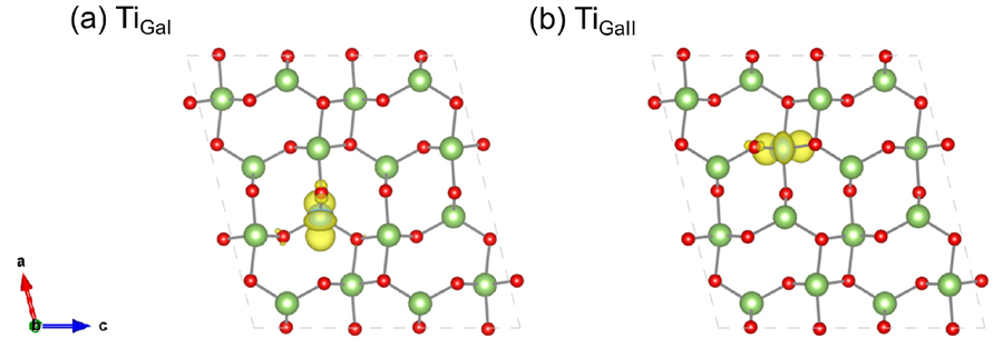
Fig. 1. (Color online) The partial charge density of the defect states of (a) TiGaI (substitute on the tetrahedral site) and (b) TiGaII (substitute on the octahedral site) defects in
![(Color online) The defect transition levels of TiGa and FeGa inβ-Ga2O3 predicted by the first-principles calculations compared with the defect signaturesE1,E2,E3 observed in DLTS measurements[4]. All energy levels are referenced to the CBM, which is 4.9 eV above the VBM and gives rise toβ-Ga2O3 a bandgap of 4.9 eV.](/richHtml/jos/2022/43/11/112801/112801-2.jpg)
Fig. 2. (Color online) The defect transition levels of TiGa and FeGa in
4 ]. All energy levels are referenced to the CBM, which is 4.9 eV above the VBM and gives rise to
Fig. 3. (Color online) First-principles-calculatedσn as a function of the transition levelεi/f for TiGa and FeGa at 300 K. The vertical arrows pointed out theσn using the calculated transition levelsεi/f inTable 3 . The energy is referenced to the CBM which is 0 eV.
Fig. 4. (Color online) Items in |VC|2 for TiGa and FeGadefects. Ph-DOS as a function of phonon frequency for the supercell containing (a) TiGa and (b) FeGa. The coupling constant |VC|2 as a function of phonon frequency in the electron-phonon coupling with (c) TiGaI, (d) TiGaII, (e) FeGaI, and (f) FeGaII.
Fig. 5. (Color online) The formation energy of TiGa and FeGa defects as a function of Fermi level under (a) O-poor conditions and (b) O-rich conditions. The Fermi energy is referenced to CBM which is set to 0 eV.
Fig. 6. (Color online) Schematic diagram forσn(εi/f) ofE2 candidates with proper reorganization energyλ.εi/f is referenced to CBM which is 0 eV at the right of the horizontal axis. The experimental defect level ofE2 is 0.74 eV[4 ] below the CBM, shown as the vertical dotted line. The horizontal dotted lines indicate the minimum and maximum experimentalσn((0.3–3) × 10–15 cm2[4 ]) ofE2. For the candidates, the downward “parabola” is intrinsic and the maximumσn remains still (see the black curve which is for FeGaII fromFig. 3 ), while the reorganization energy can be adjusted through shifting the “parabola” curve left (increasingλ) and right (decreasingλ). Meanwhile,σn of the blue and red curves at 0.74 eV should be within the experimental range,σn ofE2, to give the reorganization energy at ~1.4 eV (left shifting) and ~0.1 eV (right shifting), respectively.
|
Table 0. First-principles calculated results of TiGa and FeGa defects in
| ||||||||||||||||||||||||||||||||
Table 0. Lattice parameters (
|
Table 0. Compilation of energy levels (below the CBM and unit in eV) and electron capture cross-sections of three significant defect traps in

Set citation alerts for the article
Please enter your email address
© Copyright 2018-2021 | Chinese Laser Press. All Rights Reserved 沪ICP备15018463号-20