Abstract
The emerging wide bandgap semiconductor -Ga2O3 has attracted great interest due to its promising applications for high-power electronic devices and solar-blind ultraviolet photodetectors. Deep-level defects in -Ga2O3 have been intensively studied towards improving device performance. Deep-level signaturesE1,E2, andE3 with energy positions of 0.55–0.63, 0.74–0.81, and 1.01–1.10 eV below the conduction band minimum have frequently been observed and extensively investigated, but their atomic origins are still under debate. In this work, we attempt to clarify these deep-level signatures from the comparison of theoretically predicted electron capture cross-sections of suggested candidates, Ti and Fe substituting Ga on a tetrahedral site (TiGaI and FeGaI) and an octahedral site (TiGaII and FeGaII), to experimentally measured results. The first-principles approach predicted electron capture cross-sections of TiGaI and TiGaII defects are 8.56 × 10⁻¹⁴ and 2.97 × 10⁻¹³ cm2, in good agreement with the experimental values ofE1 andE3centers, respectively. We, therefore, confirmed thatE1 andE3 centers are indeed associated with TiGaI and TiGaIIdefects, respectively. Whereas the predicted electron capture cross-sections of FeGa defect are two orders of magnitude larger than the experimental value of theE2, indicatingE2 may have other origins like CGaand Gai, rather than common believed FeGa.The emerging wide bandgap semiconductor -Ga2O3 has attracted great interest due to its promising applications for high-power electronic devices and solar-blind ultraviolet photodetectors. Deep-level defects in -Ga2O3 have been intensively studied towards improving device performance. Deep-level signaturesE1,E2, andE3 with energy positions of 0.55–0.63, 0.74–0.81, and 1.01–1.10 eV below the conduction band minimum have frequently been observed and extensively investigated, but their atomic origins are still under debate. In this work, we attempt to clarify these deep-level signatures from the comparison of theoretically predicted electron capture cross-sections of suggested candidates, Ti and Fe substituting Ga on a tetrahedral site (TiGaI and FeGaI) and an octahedral site (TiGaII and FeGaII), to experimentally measured results. The first-principles approach predicted electron capture cross-sections of TiGaI and TiGaII defects are 8.56 × 10⁻¹⁴ and 2.97 × 10⁻¹³ cm2, in good agreement with the experimental values ofE1 andE3centers, respectively. We, therefore, confirmed thatE1 andE3 centers are indeed associated with TiGaI and TiGaIIdefects, respectively. Whereas the predicted electron capture cross-sections of FeGa defect are two orders of magnitude larger than the experimental value of theE2, indicatingE2 may have other origins like CGaand Gai, rather than common believed FeGa.Introduction
| Parameter | Defect | TiGaI | TiGaII | FeGaI | FeGaII |
|---|
| (eV) | Cal. | (+/0) 0.59 | (+/0) 1.08 | (0/–) 0.61 | (0/–) 0.74 |
| Refs. [10,11] | 0.60 | 1.13 | 0.62 | 0.72 |
| (amu1/2/Å) | Cal. | 2.06 | 1.42 | 1.61 | 1.32 |
| Refs. [10,11] | ~2.0 | 1.35 | 1.63 | 1.22 |
| (eV) | | 1.06 | 0.81 | 0.76 | 0.70 |
| (eV2) | Cal. 300 K | 0.58 | 0.56 | 0.43 | 0.48 |
| (cm2) | Cal. 300 K | 8.56 × 10⁻¹⁴ | 2.97 × 10⁻¹³ | 4.23 × 10⁻¹³ | 6.42 × 10⁻¹³ |
Table 0. First-principles calculated results of TiGa and FeGa defects in
-Ga2O3. The transition levels
and the configuration difference
are in comparison with those reported in the literature. Reorganization energies
, electron-phonon coupling constants
, and electron capture cross-sections
of TiGa and FeGa are included.
Monoclinic gallium sesquioxide (
-Ga2O3) has drawn a lot of attention due to its ultra-wide bandgap (~4.9 eV) and ultra-high breakdown electrical fields, which make it promising in the application of power electronics and deep-ultraviolet optoelectronics[1,2]. In particular, it owns a high Baliga’s figure of merit more than four times that of GaN and SiC[1], making it to be an excellent candidate for power semiconductor devices operating in high-frequency circuits[1,2]. Besides, the
-Ga2O3 devices have the advantages of high radiation hardness, high-temperature stability, potentially low cost due to the earth-abundant material, and ease to manufacture massively due to its compatibility with Si microelectronic technology. In the application of semiconductors, defects can significantly influence the performance of devices. For example, they may bring in deep levels inside the bandgap to trap the carriers or even become the nonradiative recombination centers to kill the free carriers, deteriorating the performance of devices[3].
In
-Ga2O3, three signature levels (E1,E2, andE3) have been frequently observed in the deep-level transient spectroscopy (DLTS) measurements irrespective of different types of measured
-Ga2O3 samples, including bulk crystals grown by the Czochralski method (CZ)[4] and edge-defined film-fed growth (EFG)[5], and epitaxial thin films fabricated by metalorganic chemical vapor deposition (MOCVD)[6] and hydride vapor phase epitaxy (HVPE)[7]. Specifically,E1 is 0.55–0.63 eV,E2 is 0.74–0.81 eV, andE3 is 1.01–1.10 eV below the conduction band minimum (CBM) of
-Ga2O3[4–7]. The DLTS measurements also obtained the electron capture cross-sections, which are 10–14–10–13, 10–16–10–15, and 10–14–10–13 cm2[4,5,7], respectively, for these three signature levels.Table 1 summarizes these experimentally measured defect signature levels and corresponding electron capture cross-sections. These signature levels have been assigned to different types of defects, such as intrinsic defects or extrinsic impurities[8]. For instance, (i) the origin of theE1 andE3 centers used to be regarded as the transition metal impurities presenting at the Ga lattice sites[9], including FeGa and CoGa[4]. (ii) TheE2 center was initially suggested to be the FeGa defects by Ingebrigtsenet al.[8]. Zimmermanet al.[10] further distinguished that there are two overlapping DTLS peaks, labeled asE2a (0.66 eV) andE2b (0.73 eV) instead of a singleE2. These two signatures have then been assigned to the Fe substituting Ga on a tetrahedral site (FeGaI) and an octahedral site (FeGaII), respectively, based on the energy levels and the concentration ratio[10]. Recently, Zimmermannet al.[11] provided additional evidence to support the above conclusion regarding the good agreement of absorption cross-section between first-principles calculations of the FeGa defect and the experimental results from steady-state photo-capacitance spectra measurements. (iii) TheE3 trapping center has been suggested as oxygen vacancy (VO)[12], or substitutional transition-metal defects (e.g., FeGa or TiGa)[9]. However, the calculated VO defect level is located at 1.67–2.46 eV (below the CBM)[13], which is much deeper thanE3 at 1.01–1.10 eV and thus can be ruled out. Zimmermanet al.[10] then assigned theE3 center as a defect of Ti substituting Ga on an octahedral site (denoted as TiGaII) based on a strong correlation in concentration between theE3defect and the Ti ions present in the samples and a good agreement in energy position between theE3 level and the TiGaII defect, which is obtained by the hybrid functional calculations. So far, Fe- and Ti-related defects are considered as the most possible candidates forE1,E2, andE3 centers not only due to the above arguments but also because they can be introduced to
-Ga2O3 unintentionally in fabrications. For example, Fe is the most common contaminant in manufacturing. Ti is often used as Ohmic contact for
-Ga2O3 devices[1,14]. However, most identifications are made based purely on matching the energy levels, which could be accidental.
Generally, the DLTS is a highly sensitive analytical technique that is used to measure the energy positions of defects and obtain the carrier capture cross-sections, but without the capability to obtain information about the configuration and elements of the defects[4]. The first-principles calculations are therefore used to explore the atomic origin of these defect levels by examining their defect levels. One challenge in previous theoretical studies of the defect levels is that only the predicted transition energies can be compared with experimental data. Therefore, the identification of the atomic origin for a special defect level is still a difficult task. Fortunately, the newly developed first-principles approach for carrier capture cross-sections enables us to examine the defect candidates utilizing a combination of both the energy level and carrier capture cross-section for each center. In this work, we use this approach to verify the well-established defect candidates of TiGa and FeGa for the three signatures in
-Ga2O3 by performing the first-principles calculations for both defect transition level and electronic capture cross-section. The calculated transition levels of TiGaI and TiGaII from a charge stateq= +1 to a charge stateq= 0 are 0.59 and 1.08 eV below the CBM within the ranges of DLTS measuredE1 (0.55–0.63 eV) andE3 (1.01–1.10 eV), respectively. This excellent agreement is consistent with previous first-principles calculations[10]. In particular, the calculated electron capture cross-sections of TiGaI and TiGaII defects are both around 10–14–10–13 cm2 and thus are also in excellent agreement with experimental results ofE1 andE3 centers[4,5,7,10,15]. Subsequently, we can safely conclude that the TiGaI and TiGaII defects are responsible for DTLS observed E1 andE3 centers, respectively. However, the calculated electron capture cross-section of FeGa defects is around 10–13 cm2, which is about two orders of magnitude larger than that of DLTS measuredE2 center. Such large disagreement indicates thatE2 has other origins than FeGa, although the defect levels of FeGaare in good agreement with theE2 (orE2a, andE2b) center.
Method
In this work, all the first-principles calculations were performed using the PWMAT[16,17] package with the SG15 collection of the optimized norm-conserving Vanderbilt pseudopotentials (ONCV)[18] with an energy cutoff of 70 Ryd. Heyd-Scuseria-Ernzerhof (HSE)[19] screened hybrid functional was applied for all the calculations except the calculations of electron-phonon coupling constants which used the Perdew-Burke-Ernzerhof functional of the generalized gradient approximation (GGA-PBE). The Ga-4s, -4p, Ti-3s, 3p, -3d, -4s, and Fe-3s, -3p, -3d, -4s electrons were included as valence electrons. The fraction of the screened Hartree-Fock exchange was adjusted to
= 0.33 to reproduce the experimental band gap of 4.9 eV. The lattice parameters of the pure
-Ga2O3 were predicted to be
= 12.20 Å,b = 3.03 Å, andc = 5.78 Å with
= 103.8
, as shown inTable 2. A 160-atom (
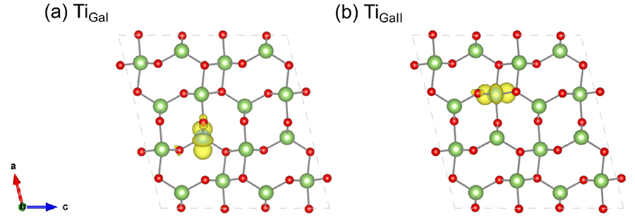
) supercell is adopted to calculate defects with a Gamma-onlyk-point mesh for integration over the Brillouin zone.Fig. 1 shows the atomic configuration of one Ti substituting one Ga atom on the tetrahedral site (TiGaI) and the octahedral site (TiGaII), respectively, in
-Ga2O3. The defect of Fe substitution of Ga (FeGa) has the same configurations as TiGa except for the replacement of Ti by Fe. We have considered spin polarization for the incorporation of Fe ions in the first-principles calculations. Fe substituting Ga atom in +3
and +2 (S = 2) states[8,20] are labeled as
and
.

Figure 1.(Color online) The partial charge density of the defect states of (a) TiGaI (substitute on the tetrahedral site) and (b) TiGaII (substitute on the octahedral site) defects in
-Ga2O3.
| Parameter | Defect | TiGaI | TiGaII | FeGaI | FeGaII |
|---|
| (eV) | Cal. | (+/0) 0.59 | (+/0) 1.08 | (0/–) 0.61 | (0/–) 0.74 |
| Refs. [10,11] | 0.60 | 1.13 | 0.62 | 0.72 |
| (amu1/2/Å) | Cal. | 2.06 | 1.42 | 1.61 | 1.32 |
| Refs. [10,11] | ~2.0 | 1.35 | 1.63 | 1.22 |
| (eV) | | 1.06 | 0.81 | 0.76 | 0.70 |
| (eV2) | Cal. 300 K | 0.58 | 0.56 | 0.43 | 0.48 |
| (cm2) | Cal. 300 K | 8.56 × 10⁻¹⁴ | 2.97 × 10⁻¹³ | 4.23 × 10⁻¹³ | 6.42 × 10⁻¹³ |
Table 0. First-principles calculated results of TiGa and FeGa defects in
-Ga2O3. The transition levels
and the configuration difference
are in comparison with those reported in the literature. Reorganization energies
, electron-phonon coupling constants
, and electron capture cross-sections
of TiGa and FeGa are included.
We use a well-established set of approaches[27,28] to calculate the formation energies and transition levels
of the defects based on the first-principles calculations of total energy. Specifically, for charged defects, we utilize the image charge interaction correction with the approximation method (C-AP) proposed in Ref. [29] to obtain the defect formation energy as follows,
Here,
is the total energy of a supercell containing the defect
in a charge stateq,
is the C-AP correction term,E(host) is the total energy of the bulk host supercell without defect, andni is the number of atoms with chemical potentialμi added (ni \gt 0) to or removed (ni \lt 0) from the supercell to create the defect. The chemical potential of Ga(μGa) is in a range with its upper and lower bound setting by bulk elemental Ga (Ga-rich) and the stability condition of Ga2O3 (Ga-poor), respectively. The chemical potential of Fe(μFe) is in a range determined by Ga3Fe and Fe2O3[8] andμTi is determined by TiO2. The Fermi level
is referenced to
the valence band maximum (VBM) of the host (here is Ga2O3) with its potential aligned with the potential of defect supercell at the corner (farthest away from the defect). The transition level from the initial statei in a charge state
to the final statef in a charge state
is the difference of their formation energy per charge when their Fermi levels equal,
For the transition levels
close to the CBM, we transform them to referring to the CBM in terms of
.
To calculate the nonradiative carrier capture cross-sections of defects, we then utilize the recently developedab initio multi-phonon method for nonradiative decay rates[30–33] based on the multi-phonon recombination theory from Kun Huang[34–36], which has been implemented in the PWMAT[16,17] package. Specifically, the nonradiative decay probability from the initial electronic statei to the final electronic statef is[30]
where
is the defect transition level measured from CBM,
the reorganization energy induced by the electron transfer fromi tof states, and
the eigenvector of the phonon modes. The corresponding coordinate difference
can be obtained in terms of
, where
is atom index in the supercell,
is the nuclear mass, and
the atomic displacement. The summation term in Eq. (3) is defined as an electron-phonon coupling constant
, which indicates that the perturbation
caused by atomic displacement due to random thermal vibrations can induce coupling between electronic statesi andj[30]. Once we get the nonradiative recombination probability
according to Eq. (3), we can further compute the carrier capture rate coefficient
(where
is the volume of the supercell), which is divided by the average thermal velocity
(where
is Boltzmann constant,T is temperature, andm* is the carrier effective mass) to finally obtain the carrier capture cross-section
. In
-Ga2O3, the electron effective mass is
[37] and thus, at temperature
= 300 K,
is 2.44 × 107 cm/s, which is very close to the reported electron velocity of ~2 × 107 cm/s in Ref. [38].
Results and discussion
We have considered the substitutions of Ga atom on both tetrahedral (TiGaI and FeGaI) and octahedral sites (TiGaII and FeGaII). To investigate the capture of electrons by defect levels, we study the +/0 charge transition for TiGa and 0/– transition for FeGa. Our first-principles calculated transition levels and electron capture cross-sections of TiGa and FeGa defects are given inTable 3, in comparison with available results reported in the literature. Our calculated defect levels
of TiGaI and TiGaII are 0.59 and 1.08 eV (below the CBM of
-Ga2O3), within the range of ~0.05 eV of previously reported first-principles calculations (0.60 and 1.13 eV for TiGaI and TiGaII, respectively)[10]. For FeGaI and FeGaII, our predicted transition levels
are 0.61 and 0.74 eV below the CBM, respectively. They are in excellent agreement with previously reported first-principles results, 0.62 and 0.72 eV[17], respectively. It is ready to learn that both the TiGa and FeGa defects presenting at the Ga octahedral site (GaII) have deeper energy levels than those at the Ga tetrahedral site (GaI). To assess the trapping center assignment based on defect levels, we align our calculated TiGa and FeGa defect transition levels with the DLTS measured defect signaturesE1,E2,E3, as shown inFig. 2. From the alignment of energy levels alone, we indeed see that TiGaI, FeGaII, and TiGaII can be correlated withE1,E2, andE3 trapping centers, respectively, which is consistent with previous assignments[8,10].
Figure 2.(Color online) The defect transition levels of TiGa and FeGa in
-Ga2O3 predicted by the first-principles calculations compared with the defect signaturesE1,E2,E3 observed in DLTS measurements[4]. All energy levels are referenced to the CBM, which is 4.9 eV above the VBM and gives rise to
-Ga2O3 a bandgap of 4.9 eV.
| Parameter | Defect | TiGaI | TiGaII | FeGaI | FeGaII |
|---|
| (eV) | Cal. | (+/0) 0.59 | (+/0) 1.08 | (0/–) 0.61 | (0/–) 0.74 |
| Refs. [10,11] | 0.60 | 1.13 | 0.62 | 0.72 |
| (amu1/2/Å) | Cal. | 2.06 | 1.42 | 1.61 | 1.32 |
| Refs. [10,11] | ~2.0 | 1.35 | 1.63 | 1.22 |
| (eV) | | 1.06 | 0.81 | 0.76 | 0.70 |
| (eV2) | Cal. 300 K | 0.58 | 0.56 | 0.43 | 0.48 |
| (cm2) | Cal. 300 K | 8.56 × 10⁻¹⁴ | 2.97 × 10⁻¹³ | 4.23 × 10⁻¹³ | 6.42 × 10⁻¹³ |
Table 0. First-principles calculated results of TiGa and FeGa defects in
-Ga2O3. The transition levels
and the configuration difference
are in comparison with those reported in the literature. Reorganization energies
, electron-phonon coupling constants
, and electron capture cross-sections
of TiGa and FeGa are included.
Based on the calculated transition levels
given inTable 3, we then predicted the electron capture cross-sections
of TiGaI and TiGaII defects at 300 K by performing the first-principles calculations according to Eq. (3).Table 3 shows that
of TiGaI is 8.56 × 10⁻¹⁴ cm2 and of TiGaII is 2.97 × 10⁻¹³ cm2. These two data are well within the range 10–14–10–13 cm2 of experimental data ofE1 andE3 centers (compiled inTable 1)[4,5,7]. Note that these are cross-sections for electron trapping from the original positive defect and hence could have a correction factor due to the long-range Coulomb interaction between defect and electron[39], which makes the concentration of the electron carriers near the defect larger than the average carrier density. The exact value of this correction factor depends on many factors, including the static dielectric function, the carrier concentration, the carrier effective mass, and temperature. In previous studies[39], this factor was found to be within 1 and 10 for oxides. After considering this correction factor, these calculated decay cross-sections for TiGaI and TiGaII are still within the experimental range ofE1 andE3 centers. Based on this, we thus conclude that the atomic origin of theE1 trapping center is TiGaI and theE3 trapping center is TiGaII. WhereasTable 3 shows that the electron capture cross-sections
of FeGaI and FeGaII at 300 K are 4.23 × 10⁻¹³ and 6.42 × 10⁻¹³ cm2, respectively. Note, for the initial neutral defect, the above-mentioned correction factor is close to 1. Therefore, the electron capture cross-sections of FeGaI and FeGaII defects are at least two orders of magnitude larger than the experimental value of 10–16–10–15 cm2 forE2 center[4,5,7]. Such substantial disagreement in the electron capture cross-section rules out the FeGa defect as theE2 center, although from the energy level comparison we can assign FeGaII as theE2 center or FeGaI and FeGaII as theE2a andE2b levels, respectively.
Nevertheless, before overturning the previous assignment for theE2 center[8,10], it is necessary to examine whether the computational uncertainties in the transition level and the coupling term can cause such a big disagreement in the electron capture cross-section between theE2 center and its candidate FeGa. First, the calculated coordinate difference
in the charge transitions are 2.06 (TiGaI), 1.42 (TiGaII), 1.61 (FeGaI), and 1.32 (FeGaII) amu1/2/Å respectively, which are consistent with the previous first-principles calculations presented in Refs. [10,11]. This confirms that our supercell configurations and energy level calculations are aligned with the literature.
We then inspect the effect of energy level uncertainty on the electron capture cross-sections of defect candidates.Fig. 3 shows the calculated electron capture cross-sections
of TiGa and FeGa as a function of the defect transition level
at 300 K, which is an artificially rigid shift inside the host Ga2O3 bandgap from VBM to CBM.
of TiGa and FeGa changes from ~10–19 to ~10–12 when
varies from ~2.4 eV below CBM to CBM. Note that the peak position corresponding to the reorganization energy
can also be written down as
[30] with the Huang-Rhys’ factorS[35,36]. At the peak position,
and
will get the maximum value because the defect level
equals the reorganization energy
and then
. As we can see, the maximum
for these defects are almost at the same magnitude, so
for each defect is finally determined by the exponential term, more specifically the energy difference between
and
.Table 3 shows the transition level
of defects is very close to its reorganization energy, except for TiGaI whose
is ~0.5 eV lower than
. Thus, the carrier capture cross-sections
are relatively high for the TiGaII, FeGaI, and FeGaII defects, mostly in the magnitude of 10–13 at 300 K, while
of TiGaI is a little smaller. These are relatively strong trappings of electrons and indicate the importance of these defects for carrier dynamics. In comparison, the defects in another typical wide-bandgap semiconductor SiC have much smaller trapping rates; for example, the electron capture cross-sections of defects such as VC, VSi, VC–VSi, and NC–VSi in 4H-SiC are all less than the order of 10–15[3].Fig. 3 shows the dependence of
on
for each defect shares the same variation tendency and shape, indicating that the differences induced by the transition metal atoms Ti and Fe can be small. Thus,
of TiGa and FeGa are in a similar order of magnitude.
Figure 3.(Color online) First-principles-calculatedσn as a function of the transition levelεi/f for TiGa and FeGa at 300 K. The vertical arrows pointed out theσn using the calculated transition levelsεi/f inTable 3. The energy is referenced to the CBM which is 0 eV.
We finally examine the effect of the electron-phonon coupling term
for the capture cross-sections via comparing FeGa and TiGa defects.Table 3 shows that
for TiGaI and TiGaII defects are 0.58 and 0.56 eV2, respectively, and for FeGaI and FeGaII defects are 0.43 and 0.48 eV2, respectively. The difference between two nonequivalent sites is tiny for each defect and the difference between TiGa and FeGa is also small. To gain insight into their similarity in the magnitude of
, we further evaluate the phonon mode and wavefunction of the defects, which govern the electron-phonon coupling constant
.Fig. 4(a) shows the phonon density of states (ph-DOS) for the system containing TiGaI and TiGaII, respectively. One can find that the different substituting sites will not induce a sizable change in the ph-DOS. This is also true for the FeGa defect as shown inFig. 4(b). It is even more interesting to note that the FeGa defects resemble their ph-DOS with TiGa defects, indicating the change in the impurity atom seldom affects the ph-DOS of the system. One main factor is that they have similar ionic radius due to Fe and Ti. In the 6-fold coordination configuration, the ionic radius of the Ti impurity changes from 0.68 to 0.76 Å from Ti4+ to Ti3+, and the ionic radius of the Fe impurity changes from 0.64 to 0.74 Å from Fe3+ to Fe2+[40]. As for the electronic property,Fig. 1 shows that the partial charge densities of the TiGaI and TiGaII defect states are very similar because they both originate from the Ti 3d orbitals. It is also expected to be the same in the FeGa defects where the defect states stem from the Fe 3d orbitals. Subsequently, the effective phonon modes involving the electron-phonon coupling are also similar, even though there may have small differences in strength among these four defects, as shown inFigs. 4(c)–4(f). These above features result in the close
for TiGaI and TiGaII, as well as for FeGaI and FeGaII. The change from Ti to Fe is unlike to remarkably alter the
.
Figure 4.(Color online) Items in |VC|2 for TiGa and FeGadefects. Ph-DOS as a function of phonon frequency for the supercell containing (a) TiGa and (b) FeGa. The coupling constant |VC|2 as a function of phonon frequency in the electron-phonon coupling with (c) TiGaI, (d) TiGaII, (e) FeGaI, and (f) FeGaII.
Although the reorganization energy
of these defects varies from 0.7 to 1.06 eV as listed inTable 3,Fig. 3 shows that, for all the defects, the maximum of
at
are in the same order of magnitude, which are 0.94 × 10¹⁶, 1.04 × 10¹⁶, 0.83 × 10¹⁶, and 0.97 × 10¹⁶ s–1 for TiGaI, TiGaII, FeGaI, and FeGaII, respectively. The similarities in the ph-DOS, the defect charge density from the 3d orbital, and the similar impurity ion radius all contribute to the above similarity for the maximum capture rate. The similarity of the maximum
and the fact that their transition level energy is close to the reorganization energy λ result in a similar magnitude of
around 10–13 cm2 for FeGa and TiGa defects. Based on this analysis, it is clear that FeGa and TiGa cannot have dramatically different
. Even if there are some computational uncertainties, these uncertainties should equally apply to both FeGa and TiGa. We have concluded TiGaI and TiGaII are responsible forE1 andE3, respectively. Thus, the apparent difference (two orders of magnitude) in experimentally measured
betweenE1 (orE3) andE2 might be used as evidence for excluding FeGa from the assignment toE2.
From the perspective of the defect formation energy, we can also argue that the FeGa defects are relatively unlike to form due to their high formation energy. Note that
-Ga2O3 is generally an n-type semiconductor.Fig. 5 exhibits that, to form the TiGa (E1 andE3) defects clearly, the system must be in an O-poor condition (otherwise, the TiGa formation energy can be as high as 2–3 eV). Under this O-poor condition, the literature has reported that the formation energies of both FeGaI and FeGaII are always higher than both TiGaI and TiGaII[8,10]. Our calculations also show that the formation energy of FeGa is higher than that of TiGa if the Fermi level is ~0.8 eV below the CBM. The difference occurs only in the case of high n-type doping.Fig. 5(a) shows that the formation energy of TiGaI will raise over those of both FeGaI and FeGaII, while TiGaII remains smaller than the formation energy as the Fermi level increases towards CBM due to heavier n-type doping, which argues for the unfavorable formation of FeGa. Experimental measurements have observed[41] that electron trapping centersE2 andE3 have a comparable concentration of (2–4) × 1016 cm−3, butE1 has one order of magnitude lower concentration (3 × 10¹⁴–6 × 1015 cm−3)[41]. Our predicted higher formation energy of TiGaI (E1) than that of TiGaII (E3), as shown inFig. 5(a), clearly explains the concentration difference betweenE1 andE3 centers. However, the high formation energy of FeGa (E2) renders it impossible to have a comparable high concentration as TiGaII (E3). Subsequently, we can safely rule out the FeGa defects as the atomic origin of theE2 center, which is the dominant electron trapping center and presents in all
-Ga2O3 samples.
Figure 5.(Color online) The formation energy of TiGa and FeGa defects as a function of Fermi level under (a) O-poor conditions and (b) O-rich conditions. The Fermi energy is referenced to CBM which is set to 0 eV.
Since we have ruled out the assignment of FeGa as theE2 center, it must have other defects responding to it. For instance, Irmscheret al.[4] postulated thatE2 may be associated with SnGa and VO; Farzanaet al.[5] proposed C-related origins. From our understanding, we can suggest the possibleE2 candidates. We have mentioned above that the electron capture cross-sections of deep level defects in
-Ga2O3 are at least an order of magnitude larger than those in SiC. Because SiC is more covalent than
-Ga2O3, thus results in a weaker lattice vibration-induced local dipolar field and electron-phonon coupling. Hence, we expect the change of foreign atoms is unlikely to substantially change the maximum value of
at
. However, we can horizontally shift the downward “parabola” of the
by modifying the reorganization energy
, as shown inFig. 6, to remarkably reduce the
value at
.Fig. 6 shows the schematic diagram for
ofE2 candidates with proper reorganization energy
. Here, an experimental defect level ofE2 (0.74 eV[4]) is adopted, and the experimental electron capture cross-section
is (0.3–3) × 10–15 cm2[4] . These two conditions require the candidates to have the reorganization energy at ~1.4 or ~0.1 eV. This means the large atom size difference between substituting atom and the host lattice atom or even complex defects can induce strong local distortion, resulting in a large reorganization energy of ~1.4 eV. Meanwhile, a defect with very small reorganization energy as ~0.1 eV, meaning the less atom size difference and weak local distortion, may also make sense. The first-principles calculation predicted transition level of the CGa defect is 0.81 eV below CBM[42] which is very close to theE2 level of 0.74 eV. The large difference in atom size between C and Ga is expected to induce strong distortion, which may give rise to larger reorganization energy (as large as ~1.4 eV) than 0.70 eV of FeGaII and have
curve like the blue one shown inFig. 6. Therefore, CGa is very likely responsible forE2. However, the defect level of VO is 1.67–2.46 eV below CBM[13], rather deeper than 0.74 eV; SnGa has the defect level of 0.19 eV below CBM[42] which is too shallow. Both VO and SnGa are unlikely responsible for theE2 center. Beyond these defects suggested in the literature, we find that Gai and GaOII[7], VGa–VO divacancies such as VGaII–VOI or VGaI–VOII[21] all have the defect levels at 0.7–0.9 eV below CBM and may also induce strong distortion and have large reorganization energy. Subsequently, the CGa, Gai, GaOII, and VGa–VO defects can be candidates forE2 and need to be studied further in the future.
Figure 6.(Color online) Schematic diagram forσn(εi/f) ofE2 candidates with proper reorganization energyλ.εi/f is referenced to CBM which is 0 eV at the right of the horizontal axis. The experimental defect level ofE2 is 0.74 eV[4] below the CBM, shown as the vertical dotted line. The horizontal dotted lines indicate the minimum and maximum experimentalσn((0.3–3) × 10–15 cm2[4]) ofE2. For the candidates, the downward “parabola” is intrinsic and the maximumσn remains still (see the black curve which is for FeGaII fromFig. 3), while the reorganization energy can be adjusted through shifting the “parabola” curve left (increasingλ) and right (decreasingλ). Meanwhile,σn of the blue and red curves at 0.74 eV should be within the experimental range,σn ofE2, to give the reorganization energy at ~1.4 eV (left shifting) and ~0.1 eV (right shifting), respectively.
Conclusion
We use first-principles methods to calculate the defect levels and the electron capture cross-sections of TiGa and FeGa in
-Ga2O3 which have been assigned to the experimental signaturesE1,E3, andE2centers in the literature. Using both transition level position and electron capture cross-sections as criteria, we proposed that Ti substituting for Ga on a tetrahedral site (TiGaI) and an octahedral site (TiGaII) are indeed associated withE1 andE3 states respectively. However, for the signature levelE2, the Fe substituting for Ga on a tetrahedral and an octahedral site have calculated transition level energies in good agreement with the experiment, but the calculated electron capture cross-sections are two orders of magnitude larger than the experimental results. A comparative analysis between the TiGa and FeGa defects and a computational sensitivity study of electron capture cross-sections indicate that the computational uncertainty is unlikely to cause a two order of magnitude difference in the electron capture cross-sections between TiGa and FeGa. Besides, the calculated formation energy shows it is unfavorable for the FeGa formation. All of these lead us tentatively exclude FeGa as the experimentally observedE2 signature. Thus, the exact nature ofE2 awaits future experimental and theoretical discovery.
References
[1] S J Pearton, J C Yang, P H IV Cary et al. A review of Ga2O3 materials, processing, and devices. Appl Phys Rev, 5, 011301(2018).
[2] M Higashiwaki, K Sasaki, H Murakami et al. Recent progress in Ga2O3 power devices. Semicond Sci Technol, 31, 034001(2016).
[3] Y X Gu, L Shi, J W Luo et al. Directly confirming theZ1/2 center as the electron trap in SiC through accessing the nonradiative recombination. Phys Status Solidi R, 16, 2100458(2022).
[4] K Irmscher, Z Galazka, M Pietsch et al. Electrical properties ofβ-Ga2O3 single crystals grown by the Czochralski method. J Appl Phys, 110, 063720(2011).
[5] E Farzana, M F Chaiken, T E Blue et al. Impact of deep level defects induced by high energy neutron radiation in β-Ga2O3. APL Mater, 7, 022502(2019).
[6] A Y Polyakov, N B Smirnov, I V Shchemerov et al. Compensation and persistent photocapacitance in homoepitaxial Sn-doped β-Ga2O3. J Appl Phys, 123, 115702(2018).
[7] M E Ingebrigtsen, A Y Kuznetsov, B G Svensson et al. Impact of proton irradiation on conductivity and deep level defects in β-Ga2O3. APL Mater, 7, 022510(2019).
[8] M E Ingebrigtsen, J B Varley, A Y Kuznetsov et al. Iron and intrinsic deep level states in Ga2O3. Appl Phys Lett, 112, 042104(2018).
[9] A Y Polyakov, N B Smirnov, I V Shchemerov et al. Point defect induced degradation of electrical properties of Ga2O3 by 10 MeV proton damage. Appl Phys Lett, 112, 032107(2018).
[10] C Zimmermann, Y K Frodason, A W Barnard et al. Ti- and Fe-related charge transition levels in β-Ga2O3. Appl Phys Lett, 116, 072101(2020).
[11] C Zimmermann, Frodason Y Kalmann, V Rønning et al. Combining steady-state photo-capacitance spectra with first-principles calculations: The case of Fe and Ti in β-Ga2O3. New J Phys, 22, 063033(2020).
[12] A Y Polyakov, N B Smirnov, I V Shchemerov et al. Defects responsible for charge carrier removal and correlation with deep level introduction in irradiated β-Ga2O3. Appl Phys Lett, 113, 092102(2018).
[13] C Zimmermann, V Rønning, Frodason Y Kalmann et al. Primary intrinsic defects and their charge transition levels in β-Ga2O3. Phys Rev Mater, 4, 074605(2020).
[14] M H Lee, R L Peterson. Interfacial reactions of titanium/gold ohmic contacts with Sn-doped β-Ga2O3. APL Mater, 7, 022524(2019).
[15] Z Zhang, E Farzana, A R Arehart et al. Deep level defects throughout the bandgap of (010) β-Ga2O3 detected by optically and thermally stimulated defect spectroscopy. Appl Phys Lett, 108, 052105(2016).
[16] W L Jia, J Y Fu, Z Y Cao et al. Fast plane wave density functional theory molecular dynamics calculations on multi-GPU machines. J Comput Phys, 251, 102(2013).
[17] W L Jia, Z Y Cao, L Wang et al. The analysis of a plane wave pseudopotential density functional theory code on a GPU machine. Comput Phys Commun, 184, 9(2013).
[18] D R Hamann. Optimized norm-conserving Vanderbilt pseudopotentials. Phys Rev B, 88, 085117(2013).
[19] J Heyd, G E Scuseria, M Ernzerhof. Hybrid functionals based on a screened Coulomb potential. J Chem Phys, 118, 8207(2003).
[20] S Bhandari, M E Zvanut, J B Varley. Optical absorption of Fe in doped Ga2O3. J Appl Phys, 126, 165703(2019).
[21] Y K Frodason, C Zimmermann, E F Verhoeven et al. Multistability of isolated and hydrogenated Ga-O divacancies in β-Ga2O3. Phys Rev Materials, 5, 025402(2021).
[22] J B Varley, J R Weber, A Janotti et al. Oxygen vacancies and donor impurities in β-Ga2O3. Appl Phys Lett, 97, 142106(2010).
[23] T Zacherle, P C Schmidt, M Martin. Ab initiocalculations on the defect structure of β-Ga2O3. Phys Rev B, 87, 235206(2013).
[24] J Åhman, G Svensson, J Albertsson. A reinvestigation of β-gallium oxide. Acta Crystallogr C, 52, 1336(1996).
[25] M Orita, H Ohta, M Hirano et al. Deep-ultraviolet transparent conductive β-Ga2O3 thin films. Appl Phys Lett, 77, 4166(2000).
[26] Thermochemical Data of Pure Substances. Part I + II. Von I. Barin. VCH Verlagsgesellschaft, Weinheim/VCH Publishers, New York 1989. Part I: I-1 – I 87, S. 1–816; Part II: VI, S. 817–1739; Geb. DM 680.00. — ISBN 3-527-27812-5/0-89573-866-X - Maier=1990-Angewandte Chemie-Wiley Online Library,https://onlinelibrary.wiley.com/doi/abs/10.1002/ange.19901020738
[27] C Freysoldt, B Grabowski, T Hickel et al. First-principles calculations for point defects in solids. Rev Mod Phys, 86, 253(2014).
[28] S H Wei. Overcoming the doping bottleneck in semiconductors. Comput Mater Sci, 30, 337(2004).
[29] Z J Suo, J W Luo, S S Li et al. Image charge interaction correction in charged-defect calculations. Phys Rev B, 102, 174110(2020).
[30] Y Xiao, Z W Wang, L Shi et al. Anharmonic multi-phonon nonradiative transition: Anab initio calculation approach. Sci China Phys Mech Astron, 63, 277312(2020).
[31] L Shi, L W Wang. Ab initio calculations of deep-level carrier nonradiative recombination rates in bulk semiconductors. Phys Rev Lett, 109, 245501(2012).
[32] L Shi, K Xu, L W Wang. Comparative study ofab initiononradiative recombination rate calculations under different formalisms. Phys Rev B, 91, 205315(2015).
[33] L W Wang. Some recent advances inab initio calculations of nonradiative decay rates of point defects in semiconductors. J Semicond, 40, 091101(2019).
[34] K Huang. On the applicability of adiabatic approximation in multiphonon recombination theory. J Semicond, 40, 090102(2019).
[35] Y Zhang. Applications of Huang-Rhys theory in semiconductor optical spectroscopy. J Semicond, 40, 091102(2019).
[36] K Huang, A Rhys. Theory of light absorption and non-radiative transitions inF-centres. Proc R Soc Lond A, 204, 406(1950).
[37] K Yamaguchi. First principles study on electronic structure of β-Ga2O3. Solid State Commun, 131, 739(2004).
[38] M A Mastro, A Kuramata, J Calkins et al. Perspective—opportunities and future directions for Ga2O3. ECS J Solid State Sci Technol, 6, P356(2017).
[39] A Alkauskas, Q M Yan, C G van de Walle. First-principles theory of nonradiative carrier capture via multiphonon emission. Phys Rev B, 90, 075202(2014).
[40] L H Ahrens. The use of ionization potentials Part 1. Ionic radii of the elements. Geochim Cosmochim Acta, 2, 155(1952).
[41] J Y Zhang, J L Shi, D C Qi et al. Recent progress on the electronic structure, defect, and doping properties of Ga2O3. APL Mater, 8, 020906(2020).
[42] S Lany. Defect phase diagram for doping of Ga2O3. APL Mater, 6, 046103(2018).