• Advanced Photonics
  • Vol. 4, Issue 4, 044001 (2022)
Pengfei Xu1 and Zhiping Zhou1、2、*
Author Affiliations
  • 1Peking University, State Key Laboratory of Advanced Optical Communication Systems and Networks, School of Electronics, Beijing, China
  • 2Chinese Academy of Sciences, Shanghai Institute of Optics and Fine Mechanics, Shanghai, China
  • show less
    DOI: 10.1117/1.AP.4.4.044001 Cite this Article Set citation alerts
    Pengfei Xu, Zhiping Zhou. Silicon-based optoelectronics for general-purpose matrix computation: a review[J]. Advanced Photonics, 2022, 4(4): 044001 Copy Citation Text show less

    Abstract

    Conventional electronic processors, which are the mainstream and almost invincible hardware for computation, are approaching their limits in both computational power and energy efficiency, especially in large-scale matrix computation. By combining electronic, photonic, and optoelectronic devices and circuits together, silicon-based optoelectronic matrix computation has been demonstrating great capabilities and feasibilities. Matrix computation is one of the few general-purpose computations that have the potential to exceed the computation performance of digital logic circuits in energy efficiency, computational power, and latency. Moreover, electronic processors also suffer from the tremendous energy consumption of the digital transceiver circuits during high-capacity data interconnections. We review the recent progress in photonic matrix computation, including matrix-vector multiplication, convolution, and multiply–accumulate operations in artificial neural networks, quantum information processing, combinatorial optimization, and compressed sensing, with particular attention paid to energy consumption. We also summarize the advantages of silicon-based optoelectronic matrix computation in data interconnections and photonic-electronic integration over conventional optical computing processors. Looking toward the future of silicon-based optoelectronic matrix computations, we believe that silicon-based optoelectronics is a promising and comprehensive platform for disruptively improving general-purpose matrix computation performance in the post-Moore’s law era.

    1 Introduction

    Silicon-based optoelectronics is a rapidly developing technology that aims to heterogeneously integrate photonic, optoelectronic, and electronic devices and circuits on a silicon substrate (photonic-electronic integration) to form a large-scale comprehensive on-chip system.1 Since the modulation bandwidth of silicon optical modulators exceeded 1 GHz in 2004,2 the data bitrate of transmission has been continuously increasing. Due to advantages in manufacturing cost and mass production, silicon-based optoelectronics are becoming one of the mainstream solutions in both high-speed telecommunications and data center interconnections.36 IEEE P802.3bs 400GbE7 (or even 800 GbE, 1.6 TbE) high-speed optical transceivers have attracted a wide range of interest from the optical communications industry. Novel silicon-based optoelectronic technologies also expedite the development of lidars,8,9 photonic sensors,10 optical gyroscopes,11 optical computing processors (or coprocessors), and more.

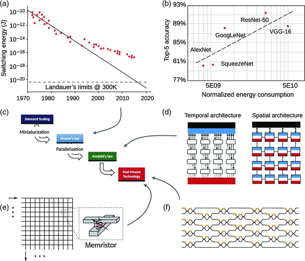
    In past decades, artificial neural network (ANN) became a popular model for image classification, pattern recognition, and prediction in many disciplines. Unlike neuromorphic computing (build neural dynamics models, mimic natural neural networks, train the plasticity of synapses, and aim at lower energy consumption brain-like artificial intelligence), ANN adopts an aggressive accuracy-driven strategy in its software research and development. Innovative ANN models, like the convolution (CONV) neural network (ALEXNET,12 VGG,13 RESNET,14 etc.) and the recurrent neural network (long short-term memory15), are proposed to achieve more accurate results. Although ANN models made revolutionary progress in artificial intelligence, the overall floating-point operations (FLOPs) of ANN models have been increasing exponentially. The parameters of these high-accuracy models are generally more than billions (or even trillions) of model parameters. The ANN model training process also requires a lot of matrix computations, which usually take several weeks in cloud data centers with large amounts of data, thereby increasing the software development life cycle. Notably, due to the slowdown of complementary metal–oxide–semiconductor (CMOS) technology scaling, Moore’s law no longer seems to apply, and the switching energy of a single transistor deviates from the law’s expectations16 [in Fig. 1(a)]. It is becoming increasingly difficult to reduce the minimum feature size of transistors and improve the single-core performance, which is limited by clock speed and energy efficiency of digital logic circuits, whereas the accuracy-driven ANN models demand higher requirements of the computation performance of the processors. Figure 1(b) shows the model accuracy versus normalized energy consumption of typical ANN models. To further increase the model accuracy in classification, model training and execution often tend to consume exponentially more electricity.17

    Development of processors for matrix computation. (a) Moore’s law no longer seems applicable.16 (b) Exponential growth of energy consumption for more accurate ANN models.17 (c) Development trends of processors.18 (d) Temporal and spatial architectures for multicore parallelization.17 (e) Memristor crossbar arrays in post-Moore’s law era.19 (f) Integrated waveguide meshes for general-purpose matrix computation.20

    Figure 1.Development of processors for matrix computation. (a) Moore’s law no longer seems applicable.16 (b) Exponential growth of energy consumption for more accurate ANN models.17 (c) Development trends of processors.18 (d) Temporal and spatial architectures for multicore parallelization.17 (e) Memristor crossbar arrays in post-Moore’s law era.19 (f) Integrated waveguide meshes for general-purpose matrix computation.20

    In recent decades [in Fig. 1(c)], multicore parallel processing electronic processors,18 including temporal architectures [e.g., graphics processing unit (GPU) based on the single-instruction multiple-data execution model] and spatial architectures [e.g., tensor processing unit (TPU) based on systolic arrays21], became the mainstream solutions for accelerating large scale matrix computations in ANNs, combinatorial optimization, compressed sensing, and digital signal processing17 [in Fig. 1(d)]. However, as suggested by Amdahl’s law,22 the overall performance gain from multicore parallelization is limited by diminishing returns; electronic processors also suffer from the tremendous energy consumption of the digital transceiver circuits during high-capacity communication with memory, storage, and peripheral hardware. In Von Neumann architecture23 processors, during computation, data and instructions need to be sent to the processor via input/output (I/O) connections. The energy consumption of digital transmitter and receiver circuits is equivalent to or much greater than the energy consumption of transistors for computation in digital logic circuits. The data connections’ energy consumption reaches the 100  fJ/bit level (depends on the distance of the copper connections) and occupies 30% to 50% of total energy use for heavy-duty matrix computations. From the perspective of electronics, the effective solution to this energy consumption is to optimize the processor architectures, reduce the unnecessary data movements, enable higher density integration, and increase the data transmission efficiency. However, electronic processors are inevitably reaching performance limitations in computational power, energy efficiency, and I/O connections.24

    Since electronic processors are approaching their limits, in post-Moore’s law era, emerging potential analog computation paradigms, like in-memory computing25 and optical computing, are being considered to surpass the performance bottleneck of electronic processors.26 For example, memristor crossbar arrays [in Fig. 1(e)] are a typical example of the in-memory computing paradigm,19 and silicon-based optoelectronic matrix computation based on integrated waveguide meshes is a typical example of optical computing [in Fig. 1(f)]. Silicon-based optoelectronic matrix computation has the following distinct characteristics and is showing great capabilities and feasibilities, which we will detail in the up-coming sections.

    2 Recent Progress in Silicon-Based Optoelectronic Matrix Computation

    Electronic processors are the mainstream and almost invincible hardware for general-purpose computation. Most of the novel research in optical computing published recently can easily be defeated by digital logic circuits in terms of energy efficiency, manufacturing cost, and reliability. Even a smartphone can run complex artificial intelligence applications with extremely low power consumption.27 Unlike versatile and multi-purpose electronic processors, optical computing has difficulty achieving complex and diverse functionalities by simply arranging and combining basic logical units (just like digital logic circuits consisting of billions of transistors). Optical computing usually needs to take advantages or specific characteristics of light waves,28 such as optical field transformation and coherent detection. By combining electronic, photonic, and optoelectronic devices and circuits together on a silicon substrate, silicon-based optoelectronic matrix computation is one of the few general-purpose computations that have the potential to surpass the computation performance of the digital logic circuits in terms of energy efficiency, computational power, latency, and maintainability. In this section, we will review the recent studies in photonic matrix computation, including matrix-vector multiplication (MVM), CONV, and MAC operation. These computations are closely interrelated, e.g., both MVM and CONV can be achieved by a series of MAC operation; the CONV between filters and kernel can be deployed in an MVM processor (in Fig. 2).

    Intuitive visualization showing energy-efficient models processing in the convolutional neural network. The CONV between the filters and kernel can be deployed into the MVM to improve efficiency.

    Figure 2.Intuitive visualization showing energy-efficient models processing in the convolutional neural network. The CONV between the filters and kernel can be deployed into the MVM to improve efficiency.

    2.1 Integrated Waveguide Meshes for MVM

    Although nowadays it is possible to achieve quantum information processing (QIP) up to tens of qubits, there are still some inconveniences (e.g., a large amount of space required, need a lot of discrete optics, work at low temperatures) in achieving large scale unitary transformation to the quantum states (i.e., programming). In 2007, the first photonic integrated two-qubit control-NOT (CNOT) gate [in Fig. 3(b)] for QIP was demonstrated on a silicon chip.30 Compared with the bulk-optical setup [in Fig. 3(a)],29 integrated waveguide meshes are more robust for practical applications. The photonic QIP chips have made great progress and are widely employed in quantum encrypted communication,41 quantum teleportation, and quantum computing.42,43 For example, Fig. 3(c) is the photonic integrated circuits chip by cascaded Mach–Zehnder interferometers (MZIs) for programmable QIP;31,44Fig. 3(d) is the large-scale chip comprising more than 200 photonic components for 98 different two-qubit operations; Fig. 3(e) is a large scale quantum circuit with more than 550 photonic components on a single chip for multidimensional quantum entanglement.

    Integrated waveguide meshes: from QIP to MVM. (a) Bulk-optical CNOT gate in 2004.29 (b) On-chip photonic CNOT gates in 2007.30 (c) Programmable quantum processor in 2016.31 (d) Large-scale photonic processor for arbitrary two-qubit operations.32 (e) Large-scale photonic processor for multidimensional quantum entanglement.33 (f) Schematic of optical switch topologies in the data center.34 (g) Reconfigurable hexagonal mesh for programmable signal processing.35 (h) Photonic “FPGA” for programmable radiofrequency signal processing.36 (i) Self-configuring 4×4-port linear processor. (j) First optical computing processor for vowel recognition.20 (k) Large scale 64×64 MVM processor.37,38 (l) FFTNet architecture for better fault tolerance against imprecise components.39 (m) Redundant architecture to overcome fabrication errors.40

    Figure 3.Integrated waveguide meshes: from QIP to MVM. (a) Bulk-optical CNOT gate in 2004.29 (b) On-chip photonic CNOT gates in 2007.30 (c) Programmable quantum processor in 2016.31 (d) Large-scale photonic processor for arbitrary two-qubit operations.32 (e) Large-scale photonic processor for multidimensional quantum entanglement.33 (f) Schematic of optical switch topologies in the data center.34 (g) Reconfigurable hexagonal mesh for programmable signal processing.35 (h) Photonic “FPGA” for programmable radiofrequency signal processing.36 (i) Self-configuring 4×4-port linear processor. (j) First optical computing processor for vowel recognition.20 (k) Large scale 64×64 MVM processor.37,38 (l) FFTNet architecture for better fault tolerance against imprecise components.39 (m) Redundant architecture to overcome fabrication errors.40

    Meanwhile, with the development of silicon-based optoelectronics technology, programmable linear processors were developed to meet more applications, such as tunable filter, microwave photonics, and all-optical switching.45 For example, optical switching networks [in Fig. 3(f)] can be realized with different kinds of network topologies programmable linear processors in data centers.34 Besides, a hexagonal cell chip [in Fig. 3(g)] for implementing arbitrary unitary transformations and signal processing,35,46 microwave photonic signal processor [in Fig. 3(h)] for continuous radiofrequency filtering and processing, and self-configuring linear processor [in Fig. 3(i)] with in-circuit optical power monitors feedback4750 have also been reported.

    Theoretically, the transfer matrix of lossless integrated waveguide meshes is a unitary matrix,51,52 then the unitary MVM can be performed.53 In recent years, integrated waveguide meshes became a feasible architecture for large-scale general purpose MVM computation in post-Moore’s law era. The first ANN proof-of-concept experiment was performed on 56 cascaded programmable MZIs meshes in 2017 [in Fig. 3(j)], and a simple vowel recognition task was demonstrated due to the limited hardware capability. In 2020, large scale 64×64 photonic-electronic copackaged MVM processors [in Fig. 3(k)] have been reported by Lightmatter, achieving 99% accuracy in ResNet-50 ImageNet classification.37 To enhance the energy consumption advantage of the matrix computation, the matrix configuration of the photonic MVM processor has recently been scaled up to 256×256, which also brings about precision problems in computation. The fabrication inconsistency in minuscule MZI devices will result in the accumulation of computation errors. Mesh optimizations are suggested to reduce the computation errors to obtain more accurate results. For example, FFTNet architecture [in Fig. 3(l)]39 and redundant architecture [in Fig. 3(m)]40 are both numerically investigated to enhance the robustness and overcome fabrication imperfections.

    2.2 Multiple Light Source MVM

    In addition to single light source schemes with a single coherent laser light source, multiple light source schemes (implemented with optical frequency comb or multiple wavelength laser arrays) are proposed in recent published studies. These are emerging methods for improving the signal-to-noise ratio of light energy and avoiding the influence of laser signal phase jitter. For example in Fig. 4(a), a microring modulators MVM scheme with 8×10⁷  MAC/s computational power was experimentally demonstrated at a clock rate of 10 MHz.54Figure 4(b) is the on-chip photorefractive interaction scheme, in which the input optical signals are sent to the photorefractive interaction region and then diffract on the photorefractive grating to perform the MVM operation.55,56 Recently, like the memristor crossbar arrays, photonic TPU and photonic crossbars arrays are becoming hot topics, both of which are potential architectures for multiple light source MVM computations. For example, Fig. 4(c) is a simulated photonic tensor core constituted by 16 fundamental dot product engines (each performs row by column pointwise MAC) to perform MVM.57Figure 4(d) is a phase change material (PCM) assisted photonic crossbar array, the matrix elements are inscribed in the state of the PCM that patches on the waveguides, with the laser array vector input, and the MVM is then performed.58 However, to obtain higher energy efficiency compared to electronic processors, the scale of the matrix configuration must be sufficiently large. In our opinion, the multiple light source MVM scheme may have difficult challenges in scaling up the matrix configuration due to the lossy photonic crossbar.

    Multiple laser source MVM. (a) MVM based on microring modulators.54 (b) MVM based on on-chip photorefractive interaction.55,56 (c) Photonic tensor core constituted by dot-product engines.57 (d) Photonic crossbar arrays with phase-change material.58

    Figure 4.Multiple laser source MVM. (a) MVM based on microring modulators.54 (b) MVM based on on-chip photorefractive interaction.55,56 (c) Photonic tensor core constituted by dot-product engines.57 (d) Photonic crossbar arrays with phase-change material.58

    2.3 Fourier Transform-based CONV

    CONV can be achieved indirectly by using Fourier transform (FT) and inverse Fourier transform (IFT) [in Fig. 5(a)]: first, pad the input sequences with zeros to the output length and then perform the FT; second, element-wisely multiply the transformed sequence in the Fourier domain; finally, perform IFT to derive the CONV results. FT can be implemented by passive photonic devices with the free-space propagation region without consuming energy, like star coupler [in Fig. 5(b)] and phase-compensated multimode interferometer (MMI) [in Fig. 5(c)]. The plasmonic structure [in Fig. 5(d)] can offer four to five orders of magnitude of enhanced processing speed due to the minuscule footprint of the device.61 Moreover, Fig. 5(e) is the on-chip Cooley-Turkey method FT executing the CONV on the order of tens of picoseconds short.62 Once the FT device is realized, then the “4f” CONV system can be realized by using a cascade of two photonic FT devices with a phase and amplitude filter mask in between. The limitation of FT-based CONV is that FT devices typically take up large on-chip space due to the need for free-space propagation. Furthermore, the insertion loss of the FT-based CONV also leads to restrictions in the matrix configuration and overall energy efficiency.

    FT-based CONV. (a) Flowchart of CONV using FT. (b) FT based on MMI coupler and compensating phase shifter arrays.59 (c) FT operation with 21×21-star coupler.60 (d) Compact surface plasmon polaritons device for FT.61 (e) CONV based on Cooley–Tukey method FT.62

    Figure 5.FT-based CONV. (a) Flowchart of CONV using FT. (b) FT based on MMI coupler and compensating phase shifter arrays.59 (c) FT operation with 21×21-star coupler.60 (d) Compact surface plasmon polaritons device for FT.61 (e) CONV based on Cooley–Tukey method FT.62

    2.4 Element-wise MAC

    Theoretically, both MVM and CONV can be realized by a series of element-wise MAC operations. For example, a basic 3×3 CONV is [in Fig. 6(a)] equivalent to nine MAC operations or 18 FLOPs. In digital logic circuits, the matrix computation is sequentially triggered by input clock signals (commonly <5  GHz). Generally, the element-wise MAC operations aim to employ wideband optoelectronic devices (e.g., microring modulators or Mach–Zehnder modulators) to achieve higher speeds up to tens of gigahertz. Although optoelectronic devices generally consume more energy than the digital logic circuits, the higher-speed MAC operations can break through the limited clock rates in electronic processors, thereby improving the “single-core performance” of computations and reducing the latency, or try to use a small amount of photons in analog element-wise MAC operation to break the energy limit of the digital computation paradigm.

    Element-wise MAC operations. (a) Basic 3×3 CONV consisting of nine MAC operations. (b) MAC based on balanced homodyne detection.63 (c) MAC based on cascaded acousto-optical modulators.64 (d) MAC based on microring modulators.65

    Figure 6.Element-wise MAC operations. (a) Basic 3×3 CONV consisting of nine MAC operations. (b) MAC based on balanced homodyne detection.63 (c) MAC based on cascaded acousto-optical modulators.64 (d) MAC based on microring modulators.65

    Element-wise MAC operations can be realized by balanced homodyne detection, microring modulators, and cascaded modulators arrays. For balanced homodyne detection [in Fig. 6(b)], input data are optically fanned out to channels, and each detector functions as a photoelectric multiplier, calculating the homodyne product and accumulating the multiplication results. The theoretical equivalent energy consumption of analog MAC can break through Landauer’s limits in the digital paradigm (2.7  aJ/MAC at 300 K) and reach as low as the 50  zJ/MAC level.63 For the cascaded acousto-optical modulator arrays [in Fig. 6(c)], with the high linearity (30  dBc signal-to-distortion ratio) acousto-optic modulation, the FASHION-MNIST classification task is performed, and the accuracy is examined similar to a 64-bit computer at a modulation speed lower than MHz.64 Although the acousto-optic modulation is limited in bandwidth, the microring scheme with electro-optic modulation [in Fig. 6(d)] is promising for higher-speed operations.65

    2.5 Dispersion-based MAC

    The photonic matrix computation can be achieved by dispersion-based MAC, in which the dispersion manipulation is usually conducted with linearly dispersive photonic waveguides (or optical fibers) and broad-spectrum laser source (or ultrashort laser pulses). For example, the reconfigurable time-wavelength plane manipulation scheme [in Fig. 7(a)] was proposed by employing a 1.1-km long dispersion fiber and 18-GHz FSR optical frequency comb to realize the 118  GigaMAC/s MAC operation, which is equivalent to 2.69  GigaMAC/s4×4 MVM and 0.5  GigaMAC/s32×32 CONV operation.66 Similarly, photonic perceptron [in Fig. 7(d)], conducted with a 13-km spool of standard single-mode fiber and 49-wavelength 49 GHz-FSR soliton crystal microcombs, was proposed to achieve 11.9 GigaFLOPs (8 bit/FLOP) MAC operations.67Figure 7(c) was a time-stretch architecture employing mode-locked ultrashort pulses, the ultrashort pulses were first broadened by a dispersive fiber, then modulated, and finally compressed by another reversely dispersive fiber to realize the MAC operations.68Figure 7(d) is a potentially 400-GHz bandwidth temporal MAC operation operated by a hydex spiral waveguide with linear group dispersion; with a dispersive photonic waveguide, temporal CONV can be realized with 200-ps operating time and 300-fs resolution.69

    MAC based on dispersion. (a) The 118 GigaMAC/s matrix operation is realized by 1.1-km long linear dispersion fiber.66 (b) 11.9 GigaFLOPs/s MAC conducted with 13-km spool of standard single-mode fiber.67 (c) Time-stretch method for MAC operations.68 (d) Temporal CONV (a series of MAC) by spiral waveguide with linear group dispersion.69

    Figure 7.MAC based on dispersion. (a) The 118 GigaMAC/s matrix operation is realized by 1.1-km long linear dispersion fiber.66 (b) 11.9 GigaFLOPs/s MAC conducted with 13-km spool of standard single-mode fiber.67 (c) Time-stretch method for MAC operations.68 (d) Temporal CONV (a series of MAC) by spiral waveguide with linear group dispersion.69

    3 Discussions and Perspectives

    3.1 Optical Interconnections in Computation Hardware

    In Von Neumann architecture processors, the memory-processor interconnections are one of the major factors influencing the overall performance [in Fig. 8(a)], especially in data-intensive applications. For example, large scale matrix multiplication (such as 1024×1024, 2048×2048, 4096×4096) usually decomposes into multiple small-scale matrix multiplication (such as 64×64, 128×128, 256×256) during processing [in Fig. 8(b)], and memory circuits are always needed for storing temporary results.71 However, in past decades, a growing performance gap between processor performance and memory bandwidth, i.e., the “memory wall” problem, has hindered high-performance computation.73

    Interconnections in processors, memory, and peripheral hardware. (a) The memory-processor interconnections are one of the major factors influencing the overall performance and the memory wall problem that has hindered high-performance computing.70 (b) Large-scale matrix multiplication is decomposed into small-scale matrix multiplications while processing.71 (c) On-chip optical transceivers are good alternatives for low-energy-budget interconnections and boosting the data movement among the computation hardware.72

    Figure 8.Interconnections in processors, memory, and peripheral hardware. (a) The memory-processor interconnections are one of the major factors influencing the overall performance and the memory wall problem that has hindered high-performance computing.70 (b) Large-scale matrix multiplication is decomposed into small-scale matrix multiplications while processing.71 (c) On-chip optical transceivers are good alternatives for low-energy-budget interconnections and boosting the data movement among the computation hardware.72

    Electronic processors are also suffering from the tremendous energy consumption of digital transceiver circuits during massive data I/O connections. Increasing the memory-processor bandwidth and energy efficiency in interconnections is an effective way to diminish the data movement problem.74 For example, in cloud data centers where GPUs are the mainstream hardware for ANN acceleration, Nvidia developed NVlink connections for increasing the interface bandwidth of GPU interconnections (up to Tb/s).75 However, when the bandwidth exceeds 10  Tb/s, the energy budgets of electrical interconnections will exceed the expectations, which is unacceptable.7678

    Instead of power-hungry electronic transceiver circuits, on-chip optical transceivers are good alternatives for low-energy-budget interconnections and boosting the data movement among the processors, memory, and peripheral hardware72 [in Fig. 8(c)]. Therefore, it is necessary to heterogeneously integrate photonic, optoelectronic, and electronic devices and circuits on the silicon substrate. Recently many studies have been performed to realize optical interconnections on a photonic-electronic integrated platform. For example, in 2015, photonic-electronic integration was demonstrated on a silicon chip, which integrated over 70 million transistors and 850 photonic components that work together to demonstrate aggregated 55  Gb/s memory bandwidth interconnections.79 In 2018, an optimized (with polycrystalline silicon) monolithic photonic-electronic integrated system on a silicon chip led to potentially >2  (Tb/s)/mm2 bandwidth densities, and the total electrical energy consumptions of the optical transmitter and receiver are 100 and 500  fJ/bit, respectively.80

    3.2 Photonic-Electronic Integration

    Optical computing has a history of nearly 70 years,81 and the optical computing products and studies with bulk optical systems have showed great potential in matrix computations. For example, Fig. 9(a) is an MVM processor released in 2003 with a 256×256  pixel resolution spatial light modulator (SLM), which has 8000  GigaMAC/s equivalent computational power;82Fig. 9(b) is a bulk-optical 4f system that could be adapted to implement CONV by placing a phase mask in the Fourier plane;83Fig. 9(c) is a diffractive deep neural network for image classification with 3D-printed multilayer phase plates.84 However, the application of optical computing processors is not as popular as using electronic processors. Bulk optical systems have many problems in terms of their computation precision, maintainability, and mass production. For example, when the bulk-optical system encounters slight vibration, the optical components may be misaligned and cause devastating problems in computation precision.

    Optical computing from bulk-optics to photonic-electronic integration. (a) SLM-based MVM processor released by Enlight in 2003.82 (b) Bulk-optical 4f-system for convolutional neural network.83 (c) Diffractive deep neural network by 3D-printed multi-layer phase mask.84 (d) 3D copackaged module for enhancing the interaction between the photonic core and electronic ASIC.34

    Figure 9.Optical computing from bulk-optics to photonic-electronic integration. (a) SLM-based MVM processor released by Enlight in 2003.82 (b) Bulk-optical 4f-system for convolutional neural network.83 (c) Diffractive deep neural network by 3D-printed multi-layer phase mask.84 (d) 3D copackaged module for enhancing the interaction between the photonic core and electronic ASIC.34

    Silicon-based optoelectronics is a photonic-electronic integrated platform that avoids the inconvenience of discrete optics; mature CMOS manufacturing processing and packaging can achieve mass production, which is an advantage that conventional optical computing does not have. Photonic-electronic copackaging [in Fig. 9(d)] is an emerging technology for comprehensive computation hardware system and enhancing the interaction between photonic core and electronic application-specific integrated circuits (ASICs).34 For example, a large-scale 64×64 copackaged MVM processor has been reported with 14-nm process ASICs chips and 90-nm process photonic core, which achieve high-performance MVM computing.37,38 By exploiting the advantages of light in linear matrix computations, the photonic core is excellent at disruptively improving the computing performance, while the electronic circuits are necessary for performing other nonlinear operations, such as driver circuits, arithmetic and logic, data storage, and activation function. In addition, thousands of on-chip photonic and optoelectronic devices, like optical modulators, photo-detectors, and MZIs, need to be precisely controlled and assisted by electronic circuits, such as modulator drivers, trans-impedance amplifiers (TIAs), serial-parallel converters, and analog-digital converters.

    3.3 Larger Scale General Purpose Matrix Computation

    When encountering a computation problem, before considering optical computing, it should be considered whether it will be faster, more economical, more energy-efficient, or more reliable than using existing electronic processors or designing new specific digital logic circuits. Silicon-based optoelectronic matrix computation processors should directly compete with its rivals, such as multicore electronic processors (such as the existing GPU, TPU, and ASIC).85,86 By combining electronic, photonic, and optoelectronic devices and circuits together, silicon-based optoelectronic matrix computation is one of the few general-purpose computations that have the potential to surpass the computation performance of the electronic processors. In digital electronic MVM processors, with larger matrix configuration, energy consumption increased proportionally to the area of the matrix (i.e., total number of elements in a matrix), and the energy consumption per MAC with FP16 or bfloat16 precision is about 1012 Joules [in Fig. 10(b)].87 In contrast, one distinctive feature is that the photonic matrix computation is realized by thermodynamically reversible coherent detection, which does not consume any energy, and the total energy consumption of matrix computation processors is merely proportional to the matrix side-length (i.e., the number of elements in a column/row or the number of input optical modulator arrays). The equivalent energy consumption per MAC operation decreases linearly as the side-length increases.63,88,89

    Energy efficiency of silicon-based optoelectronic matrix computation processor (consider all the photonic, optoelectronic, and electronic devices and circuits). (a) The equivalent energy efficiency (energy consumption per MAC operation) linearly decreases as the side-length of the matrix increases.63 (b) Expectations of future compute density and energy efficiency in silicon-based optoelectronic matrix computation (the energy efficiency depends on the matrix configuration).

    Figure 10.Energy efficiency of silicon-based optoelectronic matrix computation processor (consider all the photonic, optoelectronic, and electronic devices and circuits). (a) The equivalent energy efficiency (energy consumption per MAC operation) linearly decreases as the side-length of the matrix increases.63 (b) Expectations of future compute density and energy efficiency in silicon-based optoelectronic matrix computation (the energy efficiency depends on the matrix configuration).

    With larger matrix configuration, the advantages in total computational power, energy efficiency, and latency will be further enhanced; although thermally maintaining the static photonic matrix will consume additional energy, this static energy consumption problem can be well solved, e.g., silicon substrate removal is doable to improve the thermal modulation efficiency and reduce the static energy consumption. Considering the entire computation systems including photonic, optoelectronic, and electronic devices and circuits, some empirical evaluation results indicate that silicon-based optoelectronic matrix computation will outperform digital logic circuits in terms of energy efficiency when the matrix configuration exceeds 128×128 [in Fig. 10(a)]. Recently, the matrix configuration of the silicon-based optoelectronic matrix computation processor is scaled up to 256×256. The manufacturing and packaging of larger-scale chips are the major challenges for photonic matrix computation.

    3.4 Improve Computation Density and Computation Precision

    In silicon-based optoelectronic matrix computation processors, increasing the modulation bandwidth is an intuitive way to further improve computational power density per unit area. Although on-chip optoelectronic devices can reach modulation speeds of tens of gigahertz, passive components have limited dynamic response (<1-MHz bandwidth). Modulation speed mismatch is inevitable, and high-speed modulation is not considered to avoid high insertion loss in a large-scale passive photonic matrix. From our perspective, distributed computing may be possible to meet the requirements of larger-scale matrix multiplication, which means to increase the number of small photonic matrices, and then the large-scale matrix computation can also be realized without increasing the modulation rate of the optical matrices.

    Furthermore, integrated waveguide meshes are mostly constructed from individual MZI devices, and the footprint of the MZI is commonly about 2500  μm2. Reducing the MZI footprint will help increase the computation density, scale up the matrix configuration, and reduce the production cost of the photonic core. For example, improving the modulation efficiency of the MZI phase shifter can reduce the length of the MZI arms; employing surface plasmon polaritons or hybrid plasmon polaritons devices can break through the diffraction limit of light and reduce the area of fundamental devices.90,91

    Computation precision plays an important role in analog computation. With a larger scale matrix configuration (e.g., from 64×64, 128×128 to 256×256), the optical intensity in the integrated waveguide mesh is gradually diluted. Moreover, the fabrication inconsistency in minuscule devices will result in the accumulation of computation errors. Recently, silicon-based optoelectronic matrix computation processors tend to merely perform unitary matrix multiplication (singular value multiplication can be performed in electronic circuits). In unitary matrix multiplications, the energy of light is almost conserved without excess energy loss, which is beneficial to improving the signal-to-noise ratio and computation accuracy of matrix multiplication. Moreover, a specific redundant architecture or mesh architecture can be employed to overcome the fabrication imperfections and achieve more robust matrix computation. The computation precision needs to be enhanced with further research and development.

    3.5 Matrix Computation for Lower-Precision-Requirement Applications

    Hardware development (processor design and production) and software development (algorithm and applications) are generally carried out separately, and matrix computation processors usually have a standard application programming interface to be utilized for software development. Higher precision is a long-standing pursuit for computation hardware. It is convenient for an electronic processor to achieve 64-bit double-precision arithmetic. However, it is impossible to achieve such high precision in analog processors. At the current stage precision problems remain in silicon-based optoelectronic matrix computation processors, as computation errors are inevitable in analog computation paradigms. We need to find some applications with lower precision requirements that can run on the general-purpose processors. Although it is difficult for silicon-based optoelectronic matrix computation processors to solve high-precision arithmetic or global optimization problems, heuristic algorithms can be developed to effectively search a near-optimal solution at a reasonable compute cost in a lower-precision processor. Silicon-based optoelectronic matrix computation processors are feasible for solving some difficult problems and reducing their time-complexity, like nondeterministic polynomial (NP) time decidable/solvable problems. A certain degree of computation errors can be tolerated in the heuristic algorithms, and the slight computation inaccuracy does not affect the result.

    For example, Ising models are NP-complete problems in combinatorial optimization, and finding a minimal energy state of the Ising model (i.e., annealing) is NP-hard. Commonly, the minimal energy state of Ising models can be solved in digital processors (with heuristic algorithms) or quantum computers (with quantum annealing). Bulk-optical computing systems (such as optical fiber loops92 and spatial light modulators93) have been invented and developed to accelerate the annealing of the Ising model. A Hopfield neural network is a recurrent neural network, in which the MVM (between the binary state vector and weight matrix) can be effectively accelerated in an MVM processor with lower time complexity. By parametrically designing the evolution dynamics of the Hopfield neural network and mimicking the interactions within the nodes [in Fig. 11(a)],94 the Ising model can spontaneously evolve to an acceptable low-energy state.

    Photonic matrix computation can be used for solving some difficult problems and reducing their time complexity. (a) Heuristic recurrent algorithm for the annealing of Ising models. (b) Reconstruction of K-sparse signals in compressed sensing. (c) Very large-scale discrete Fourier transform.

    Figure 11.Photonic matrix computation can be used for solving some difficult problems and reducing their time complexity. (a) Heuristic recurrent algorithm for the annealing of Ising models. (b) Reconstruction of K-sparse signals in compressed sensing. (c) Very large-scale discrete Fourier transform.

    In compressed sensing [in Fig. 11(b)] applications, with known measurement value y and the measurement matrix A, the underdetermined equations y=AΘ need to be solved to obtain the original K-sparse coefficient vector Θ. The reconstruction of sparse coefficient vector Θ can be solved by l0 norm minimization, i.e., minΘ0, subject to  AΘ=y. The l0 norm minimization is also NP-hard, i.e., the times of linear measurements (matrix multiplications) in K-sparse signal reconstruction are O(K×logN), which needs to be accelerated with photonic matrix computation.95

    Similarly, discrete FT (DFT) [in Fig. 11(c)] is a frequently-used operation in digital signal processing and speech recognition.96 Normally, the time complexity of the DFT algorithm by unitary matrix multiplication is O(N2), and the time complexity of the Cooley–Tukey method DFT is O(N×logN). However, the time complexity of the photonic DFT matrix multiplication is only O(1), which is of great significance for reducing energy consumption and time latency.97

    4 Summary

    We reviewed the recent research on silicon-based optoelectronic matrix computations, including MVM, CONV, and MAC operations. Conventional electronic processors are still the mainstream and almost invincible hardware that is based on digital logic circuits for computation. When designing new optical computing processors (or coprocessors) for computation, the computation performance needs to outperform the digital logic circuits in terms of computational power, energy efficiency, I/O connections, and latency. Although computation errors are inevitable in analog computation paradigms, lower-precision-requirement applications (e.g., ANN, combinatorial optimization, compressed sensing, digital signal processing, and quantum information processing) can be run on the general-purpose matrix computation processors. Looking forward to the future of large-scale matrix computation in specific applications, the silicon-based optoelectronic platform can not only heterogeneously integrate photonic (e.g., integrated waveguide mesh, free space propagation region, and dispersive waveguides), optoelectronic (e.g., high-speed modulators and photodetectors), and electronic (e.g., memory circuits, driver circuits, TIAs, serial-parallel converters, and analog-digital converters) devices and circuits on a silicon substrate to fulfill the requirements of large scale matrix computation, but can also boost the low-energy-budget data movement among the processors, memories, and peripheral hardware. We believe that silicon-based optoelectronics is a promising and comprehensive platform for general-purpose matrix computation in the post-Moore’s law era.

    Pengfei Xu received his PhD from Sun Yat-Sen University, China in 2019, and was a postdoctoral fellow in School of Electronics, Peking University, China. He is now a R&D engineer at Interuniversity Micro-electronics Center (IMEC), Belgium.

    Zhiping Zhou received his PhD in Electrical Engineering from Georgia Institute of Technology, USA in 1993. He is now a distinguished professor at Peking University, China, and a distinguished principal investigator in Shanghai Institute of Optics and Fine Mechanics, Chinese Academy of Sciences, China, focusing on silicon-based optoelectronics and microsystems research and development.

    References

    [1] Z. Zhou. Silicon Based Optoelectronics(2021).

    [2] A. Liu et al. A high-speed silicon optical modulator based on a metal-oxide-semiconductor capacitor. Nature, 427, 615-618(2004).

    [3] E. Mounier, J. Malinge. Silicon photonics report—Yole Développement.

    [4] Z. Zhou et al. Development trends in silicon photonics for data centers. Opt. Fiber Tech., 44, 13-23(2018).

    [5] D. Thomson et al. Roadmap on silicon photonics. J. Opt., 18, 073003(2016).

    [6] Z. Zhou et al. Silicon photonics for advanced optical interconnections. J. Lightwave Technol., 33, 928-933(2015).

    [7] IEEE P802.3bs 200 Gb/s and 400 Gb/s Ethernet Task Force 2017.

    [8] C. P. Hsu et al. A review and perspective on optical phased array for automotive LiDAR. IEEE J. Sel. Top. Quant., 27, 1-16(2021).

    [9] J. K. Doylend, S. Gupta. An overview of silicon photonics for LIDAR. Proc. SPIE, 11285, 112850J(2020).

    [10] E. Luan et al. Silicon photonic biosensors using label-free detection. Sensors, 19, 1161(2019).

    [11] S. Srinivasan et al. Design of integrated hybrid silicon waveguide optical gyroscope. Opt. Express, 22, 24988-24993(2014).

    [12] A. Krizhevsky, I. Sutskever, G. E. Hinton. ImageNet classification with deep convolutional neural networks. Adv. Neural Info. Proc. Syst., 25, 1097-1105(2012).

    [13] K. Simonyan, A. Zisserman. Very deep convolutional networks for large scale image recognition(2015).

    [14] K. He et al. Deep residual learning for image recognition(2016).

    [15] S. Hochreiter, J. Schmidhuber. Long short-term memory. Neural Comput., 9, 1735-1780(1997).

    [16] K. Rupp. 42 years of microprocessor trend data(2018).

    [17] V. Sze et al. Efficient processing of deep neural networks: a tutorial and survey. Proc. IEEE, 105, 2295-2329(2017).

    [18] K. I. Kitayama et al. Novel frontier of photonics for data processing-photonic accelerator. APL Photonics, 4, 090901(2019).

    [19] M. A. Nahmias et al. Photonic multiply-accumulate operations for neural networks. IEEE J. Sel. Top. Quantum Electron., 26, 1-18(2020).

    [20] Y. Shen et al. Deep learning with coherent nanophotonic circuits. Nat. Photonics, 11, 441-446(2017).

    [21] N. P. Jouppi et al. In-datacenter performance analysis of a tensor processing unit. Proc. Int. Symp. Comput. Archit. (ISCA), 1-12(2017).

    [22] G. M. Amdahl. Validity of the single processor approach to achieving large scale computing capabilities. AFIPS Conf. Proc., 483-485(1967).

    [23] M. D. Godfrey. Introduction to ‘The first draft report on the EDVAC’ by John von Neumann. Ann. Hist. Comput., 15, 11-21(1993).

    [24] H. J. Caulfield, S. Dolev. Why future supercomputing requires optics. Nat. Photon., 4, 261-263(2010).

    [25] K. E. Hamilton et al. Accelerating scientific computing in the post-Moore’s era. ACM Trans. Parallel Comput., 7, 6(2020).

    [26] Z. Zhou et al. Lowering the energy consumption in silicon photonic devices and systems [Invited]. Photonics Res., 3, B28-B46(2015).

    [27] N. G. Karthikeyan et al. Mobile Artificial Intelligence Projects(2019).

    [28] H. Zhou et al. Photonic matrix multiplication lights up photonic accelerator and beyond. Light: Sci. Appl., 11, 30(2022).

    [29] J. L. O’Brien et al. Demonstration of an all-optical quantum controlled-NOT gate. Nature, 426, 264-267(2003).

    [30] A. Politi et al. Silica-on-silicon waveguide quantum circuits. Science, 320, 646-649(2008).

    [31] N. C. Harris et al. Large scale quantum photonic circuits in silicon. Nanophotonics, 5, 456-468(2016).

    [32] X. Qiang et al. Large scale silicon quantum photonics implementing arbitrary two-qubit processing. Nat. Photonics, 12, 534-539(2018).

    [33] J. Wang et al. Multidimensional quantum entanglement with large scale integrated optics. Science, 360, 285-291(2018).

    [34] Q. Cheng et al. Recent advances in optical technologies for data centers: a review. Optica, 5, 1354-1370(2018).

    [35] D. Perez et al. Silicon photonics rectangular universal interferometer. Laser Photonics Rev., 11, 1700219(2017).

    [36] L. Zhuang et al. Programmable photonic signal processor chip for radiofrequency applications. Optica, 2, 854-859(2015).

    [37] C. Ramey. Silicon photonics for artificial intelligence acceleration. IEEE Hot Chips 32 Symp., 1-26(2020).

    [38] N. C. Harris et al. Accelerating artificial intelligence with silicon photonics, 1-4(2020).

    [39] M. Y.-S. Fang et al. Design of optical neural networks with component imprecisions. Opt. Express, 27, 14009-14029(2019).

    [40] S. Pai et al. Matrix optimization on universal unitary photonic devices. Phys. Rev. Appl., 11, 064044(2019).

    [41] N. Gisin, R. Thew. Quantum communication. Nat. Photonics, 1, 165-171(2007).

    [42] J. L. O’Brien. Optical quantum computing. Science, 318, 1567-1570(2007).

    [43] E. Knill, R. Laflamme, G. J. Milburn. A scheme for efficient quantum computation with linear optics. Nature, 409, 46-52(2001).

    [44] N. C. Harris et al. Linear programmable nanophotonic processors. Optica, 5, 1623-1631(2018).

    [45] J. Carolan et al. Universal linear optics. Science, 349, 711-716(2015).

    [46] D. Pérez et al. Multipurpose silicon photonics signal processor core. Nat. Commun., 8, 636(2017).

    [47] D. A. B. Miller. Self-configuring universal linear optical component [Invited]. Photonics Res., 1, 1-15(2013).

    [48] A. Ribeiro et al. Demonstration of a 4 × 4-port self-configuring universal linear optical component. Prog. Electromagnetics Res. Symp., 3372-3375(2016).

    [49] H. Zhou et al. Self-configuring and reconfigurable silicon photonic signal processor. ACS Photonics, 7, 792-799(2020).

    [50] H. L. Zhou et al. All-in-one silicon photonic polarization processor. Nanophotonics, 8, 2257-2267(2019).

    [51] N. J. G. Fonseca. Discussion on reciprocity, unitary matrix, and lossless multiple beam forming networks. Int. J. Antenn. Propag., 2015, 946289(2015).

    [52] M. Reck et al. Experimental realization of any discrete unitary operator. Phys. Rev. Lett., 73, 58-61(1994).

    [53] W. R. Clements et al. Optimal design for universal multiport interferometers. Optica, 3, 1460-1465(2016).

    [54] L. Yang et al. On-chip CMOS-compatible optical signal processor. Opt. Express, 20, 13560-13565(2012).

    [55] L. de Marinis et al. Photonic neural networks: a survey. IEEE Access, 7, 175827-175841(2019).

    [56] S. Abel et al. Silicon photonics integration technologies for future computing systems. 24th Optoelectron. Comm. Conf. and Int. Conf. Photonics Switch. Comput., 1-3(2019).

    [57] M. Miscuglio, V. J. Sorger. Photonic tensor cores for machine learning. Appl. Phys. Rev., 7, 031404(2020).

    [58] J. Feldmann et al. Parallel convolution processing using an integrated photonic tensor core. Nature, 589, 52-58(2021).

    [59] J. Zhou. Realization of discrete Fourier transform and inverse discrete Fourier transform on one single multimode interference coupler. IEEE Photon. Technol. Lett., 23, 302-304(2011).

    [60] J. R. Ong et al. Photonic convolutional neural networks using integrated diffractive optics. IEEE J. Sel. Top. Quantum Electron., 26, 1-8(2020).

    [61] S. S. Kou et al. On-chip photonic Fourier transform with surface plasmon polaritons. Light: Sci. Appl., 5, e16034(2016).

    [62] M. Ahmed et al. Integrated photonic FFT for photonic tensor operations towards efficient and high-speed neural networks. Nanophotonics, 9, 4097-4108(2020).

    [63] R. Hamerly et al. Large scale optical neural networks based on photoelectric multiplication. Phys. Rev. X, 9, 021032(2019).

    [64] S. Xu et al. High-accuracy optical convolution unit architecture for convolutional neural networks by cascaded acousto-optical modulator arrays. Opt. Express, 27, 19778-19787(2020).

    [65] V. Bangari et al. Digital electronics and analog photonics for convolutional neural networks (DEAP-CNNs). IEEE J. Sel. Top. Quantum Electron., 26, 1-13(2020).

    [66] Y. Huang et al. Programmable matrix operation with reconfigurable time-wavelength plane manipulation and dispersed time delay. Opt. Express, 27, 20456-20467(2019).

    [67] X. Xu et al. Photonic perceptron based on a Kerr microcomb for high-speed, scalable, optical neural networks. Laser Photonics Rev., 14, 2000070(2020).

    [68] Y. Zang et al. Electro-optical neural networks based on time-stretch method. IEEE J. Sel. Top. Quantum Electron., 26, 1-10(2020).

    [69] H. Babashah et al. Temporal analog optical computing using an on-chip fully reconfigurable photonic signal processor. Opt. Laser Technol., 111, 66-74(2019).

    [70] D. Patterson et al. A case for intelligent RAM. IEEE Micro, 17, 34-44(1997).

    [71] M. Forsythe. Matrix processing with nanophotonics(2019).

    [72] Y. Arakawa et al. Silicon photonics for next generation system integration platform. IEEE Commun. Mag., 51, 72-77(2013).

    [73] A. Tsakyridis et al. 10 Gb/s optical random access memory (RAM) cell. Opt. Lett., 44, 1821-1824(2019).

    [74] K. Keeton. Memory-driven computing(2017).

    [75] NVlink(2020).

    [76] G. Keeler. Photonics in the package for extreme scalability (PIPES)(2020).

    [77] D. A. B. Miller. Rationale and challenges for optical interconnects to electronic chips. Proc. IEEE, 88, 728-749(2000).

    [78] D. A. B. Miller. Device requirements for optical interconnects to silicon chips. Proc. IEEE, 97, 1166-1185(2009).

    [79] C. Sun et al. Single-chip microprocessor that communicates directly using light. Nature, 528, 534-538(2015).

    [80] A. H. Atabaki et al. Integrating photonics with silicon nanoelectronics for the next generation of systems on a chip. Nature, 556, 349-354(2018).

    [81] P. Ambs. Optical computing: a 60-year adventure. Adv. Opt. Technol., 2010, 372652(2010).

    [82] Enlight256(2003).

    [83] J. Chang et al. Hybrid optical-electronic convolutional neural networks with optimized diffractive optics for image classification. Sci. Rep., 8, 12324(2018).

    [84] X. Lin et al. All-optical machine learning using diffractive deep neural networks. Science, 361, 1004-1008(2018).

    [85] H. T. Peng et al. Neuromorphic photonic integrated circuits. IEEE J. Sel. Top. Quantum Electron., 24, 1-15(2018).

    [86] B. Bai et al. Towards silicon photonic neural networks for artificial intelligence. Sci. China Inform. Sci., 63, 160403(2020).

    [87] N. Jouppi et al. Motivation for and evaluation of the first tensor processing unit. IEEE Micro, 38, 10-19(2018).

    [88] A. R. Totović et al. Femtojoule per MAC neuromorphic photonics: an energy and technology roadmap. IEEE J. Sel. Top. Quantum Electron., 26, 1-15(2020).

    [89] G. Wetzstein et al. Inference in artificial intelligence with deep optics and photonics. Nature, 588, 39-47(2020).

    [90] Z. Zhou et al. Silicon on-chip PDM and WDM technologies via plasmonics and subwavelength grating. IEEE J. Sel. Top. Quantum Electron., 25, 1-13(2019).

    [91] P. Sun et al. Silicon-based optoelectronics enhanced by hybrid plasmon polaritons: bridging dielectric photonics and nanoplasmonics. Photonics, 8, 482(2021).

    [92] T. Inagaki et al. A coherent Ising machine for 2000-node optimization problems. Science, 354, 603-606(2016).

    [93] D. Pierangeli, G. Marcucci, C. Conti. Large scale photonic Ising machine by spatial light modulation. Phys. Rev. Lett., 122, 213902(2019).

    [94] C. Roques-Carmes et al. Heuristic recurrent algorithms for photonic Ising machines. Nat. Commun., 11, 249(2020).

    [95] S. Foucart, H. Rauhut. A Mathematical Introduction to Compressive Sensing(2013).

    [96] S. Lin et al. FFT-based deep learning deployment in embedded systems. Proc. Des. Autom. Test Eur. Conf. Exhib., 1045-1050(2018).

    [97] A. J. Macfaden et al. An optical Fourier transform coprocessor with direct phase determination. Sci. Rep., 7, 13667(2017).

    Pengfei Xu, Zhiping Zhou. Silicon-based optoelectronics for general-purpose matrix computation: a review[J]. Advanced Photonics, 2022, 4(4): 044001
    Download Citation