Abstract
There is growing recognition that the developments in piezoresistive devices from personal healthcare to artificial intelligence, will emerge as de novo translational success in electronic skin. Here, we review the updates with regard to piezoresistive sensors including basic fundamentals, design and fabrication, and device performance. We also discuss the prosperous advances in piezoresistive sensor application, which offer perspectives for future electronic skin. There is growing recognition that the developments in piezoresistive devices from personal healthcare to artificial intelligence, will emerge as de novo translational success in electronic skin. Here, we review the updates with regard to piezoresistive sensors including basic fundamentals, design and fabrication, and device performance. We also discuss the prosperous advances in piezoresistive sensor application, which offer perspectives for future electronic skin.Introduction
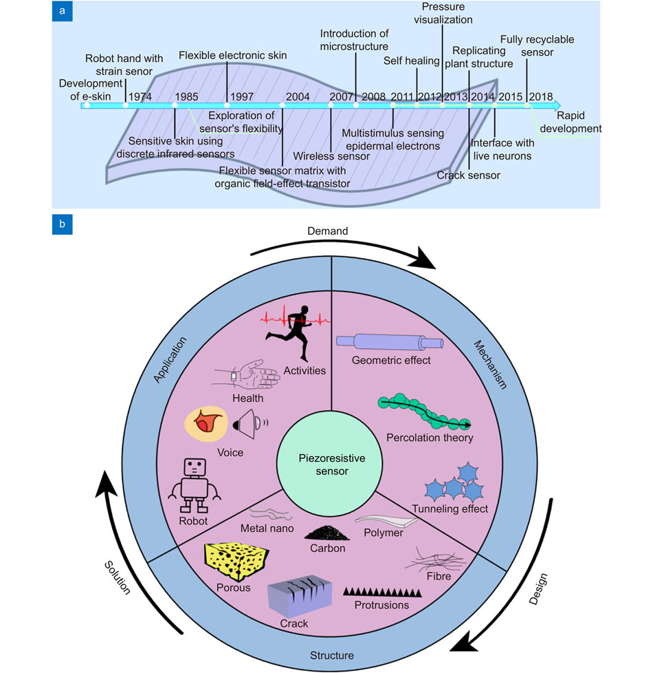
Skin is the largest organ that not only protects our bodies from the environment, but also as a system senses and converts external stimuli into physiological signals1. The concept of electronic skin (e-skin) that represents a device to mimic natural skin, is developing explosively2-4 and in order to be user friendly, it aims to rebuild the skin’s sensing response to the vital characteristic, e.g. strain, pressure, temperature, moisture, and body fluid composition, and offer enough flexible, durable and self-healing properties5-9. Historically, in 1985 General Electric developed the first skin-like electronic device to offer the sensing capability for robotic arms (Fig. 1(a))10. This progress initiates the appearance of e-skin in public vision and causes great research enthusiasm with significant developments, e.g. capabilities of shear force measurement11, spatial tactile mapping12, connection between e-skin and live neuron13, bioinspired and large-area manufacturing14-16, and self-healing property17. Meanwhile, the achievement of conductive composite makes e-skin possible to integrate flexibility with high sensitivity. For example, Lou et al.18 designed a composite for e-skin, by incorporation of reduced graphene oxide (rGO) in a flexible polymer matrix. Park et al.19 reported a ferroelectric e-skin with a complex three-dimensional (3D) microstructure, which could detect and amplify signals from temperature, pressure, and vibration change simultaneously. Latest developments on the sensitive response to sound, magnetic field, and ultraviolet light are expected to make e-skin be functional beyond natural skin20, 21. With real-time monitoring, timely feedback, wireless sensing, and ease to carry, there is a strong expectation that e-skin will display more advanced and convenient features than existing health-monitoring devices. Future e-skin shall be able to sense external stimuli and in turn crosstalk with the human neural network10, 22.

Figure 1.Piezoresistive designs for engineering electronic skin. (a) Developmental history of flexible skin-like electronics (e.g. milestones in the shear force measurement, large-area manufacturing, spatial mapping, bioinspired manufacturing, interconnection between e-skin and live neurons, and self-healing capability)10-17 . (b) Scheme illustrating the design and applications of piezoresistive sensors.
The different receptors of natural skin confer rich sensations23. A tactile sensor that mimics response to skin touch demonstrates exciting potential, for the e-skin application in wearable health-monitoring, advanced robotics, and artificial intelligence. For example, e-skin based on a tactile sensor could sense complex mechanical parameters, e.g. strength, position, and time sequence of the applied force24. Differently, e-skin based on temperature and chemical sensors could respond to thermal variation25, 26, and biofluid5, respectively. Presently, the working principle of a tactile sensor can be capacitive, piezoelectric and piezoresistive, which accounts for the sensor with a micro-level resolution to mechanical force whilst reducing manufacturing cost and complexity24. However, a capacitive sensor may associate with vulnerable sensitivity and parasitic capacitance that give the unstable performance of e-skin27, 28. A piezoelectric sensor can have the high sensitivity for precise dynamic stimulus detection, except static mechanics or the one at a magnitude beyond nanoscale29. In contrast, the piezoresistive sensor enables the detection of both static and dynamic stimulus at high sensitivity, fast response, a large sensing range and better low frequency response, and is advanced in simple assembling and low-cost fabrication30.
Current versatile designs of piezoresistive sensor find extensive research for e-skin development31, leading to the emergence of a wide range of application, including muscle contraction measurement31, gait monitoring32, voice recognition33, robotic control34 and human-machine interaction35. On the other hand, existing challenging issues toward transformation remain not solved yet and waiting for a de novo solution36. Here, we present a systemic review on the updated status of the piezoresistive sensor (Fig. 1(b)). We attempt to uncover the fundamentals, structure design, manufacturing, and performance for piezoresistive innovation. We also discuss the healthcare relevance of piezoresistive sensor-based e-skin and propose future perspectives for this field. This review has significant insights into designing advanced piezoresistive sensors for future e-skin.
Mechanisms of piezoresistive materials
By definition, the piezoresistive effect represents the change of electrical resistance under mechanical stress and strain37. It can be quantified by Gauge Factor (GF), which is equal to a ratio of the relative resistance change to applied mechanical deformation:
, where R, ρ and γ are the material’s resistance, resistivity and Poisson’s ratio, respectively38. The GF of most metallic materials is between 1.6 and 2, and under mechanical stimuli, it often varies by geometric change39. Differently, upon receiving mechanical stimuli, semiconductors can change their density and mobility of charge carriers, leading to a variation to the material’s GF40.
Piezoresistive effects from metals and conductive inorganic non-metallic materials
Metallic materials
The electrical resistance of a metal depends on its dimension and resistivity. When subjected to mechanical stimuli, the metal follows Poisson’s ratio to adjust its dimensions in length and cross-sectional area whilst giving less change to its resistivity (Fig. 2(a)). As such, the variation in metallic resistance is a function of geometric change, which forms the fundamentals of the piezoresistive effect41. For example, a metallic bent strip at a thickness of few microns has application in different strain gauges42. Such a traditional piezoresistive sensor is advanced in low-cost manufacture and high sensitivity, but remains with challenging issues when integrated into a flexible e-skin and applied for the detection in different directions43. These limitations related to metallic material could be resolved by manufacturing advances. For instance, wafer-scale microfabrication can allow for embedding metal gauge on polymer chip, thereby enabling in-situ stain monitoring44 and pressure sensing45.
Figure 2.Principles of piezoresistive effect. (a) Piezoresistance based on the geometric changes of metals and conducting polymers. i and ii represent the block and planar material geometries, respectively41,47. (b) Piezoresistance of semiconductor. Scheme illustrating the changes of charge carrier and energy band upon traction along the [111] direction in p–Si47. (c) Piezoresistance of composite materials based on the changes of conducting filler concentration and inter-filler distance48. (d) Structural piezoresistance based on the contact area and point changes of conducting architecture. Figure reproduced with permission from: (b) ref.47, Elsevier.
Further extension of piezoresistive fundamental by integration between metal and polymer, makes the wider and more convenient application of metal for the flexible device. For example, nanometal as the conductive filler can be dopped into a flexible polymer matrix and generates a piezoresistive effect by establishing percolating networks (Refer to ‘Nonconductive polymers’). Different from the direct blending, Ferreira et al.38 reported deposition of the nanostructured zigzag-like ZnO/Ag thin film on polyethylene terephthalate substrate and assembled them into a flexible and stretchable piezoresistive strain sensor. Alternatively, Peng et al.46 developed a flexible foam for piezoresistive sensor construction, by a liquid metal coating during polymerisation, and obtained a super electrical conductivity, high elasticity, and phenomenal mechanical stability (Fig. 3(a)).
Figure 3.Development of piezoresistive sensors based on various materials. (a) Fabrication scheme and optical images of a hybrid metallic foam46. (b) Schematic illustrating the fabrication of CNTs/FKM nanocomposite50. FKM, fluoroelastomer; CNTs, carbon nanotubes; and TAIC, 1,3,5-triallyl-1,3,5-triazine-2,4,6 (1H,3H,5H)-trione. (c) Scheme illustrating the assembly of a MG/PU piezoresistive sensor51. MG, modified-graphite; PU, polyurethane; and PDMS, polydimethylsiloxane. (d) A flexible tactile sensor assembled from the 8x8 array of Si-strain gauges and the Si thin film transistors64. (e) Scheme illustrating the sandwich-structure of a PEDOT:PSS/Ag NW/PDMS component film74. PEDOT:PSS, poly(3,4-ethylenedioxythiophene):poly(styrenesulfonate); and Ag NWs: Ag nanowires. (f) mGN fillers form new conducting paths under pressure80. mGN, magnetic reduced graphene oxide@nickel nanowire. Figure reproduced with permission from: (a) ref.46, (f) ref.80, American Chemical Society; (c) ref.51, under a Creative Commons Attribution 4.0 International License; (d) ref.64, AIP Publishing.
Conductive inorganic non-metallic materials
Due to the excellent comprehensive properties, carbon materials are becoming one of the most popular and competitive conductive fillers for piezoresistive sensor and e-skin development. Similar to the metallic nanomaterials, nanoscale carbon black, fibre, and tube could form piezoresistive composite for e-skin application, by direct blending with different polymers49. Shajari et al.50 developed an ultralow percolated thin film comprising of polar fluoroelastomer and carbon nanotube (Fig. 3(b)). This nanocomposite film was fabricated by an optimised internal melt-mixing process followed with common compression molding. The film was suggested to have a double-percolating electrical network that could offer simultaneous superb sensitivity for both low and high strain values and achieve a high GF of 1.3 × 10⁵ at much lower filler content (2 phr). Based on the composite comprising of graphite filler and polyurethane elastomer, He et al.51 reported a flexible piezoresistive sensor that showed high sensitivity, high reliability, and low-cost fabrication. The filler modification and concentration were found to affect the electrical conductivity of the composite films, which showed a percolation threshold at 28.03 wt% of modified-graphite and a piezoresistive sensitivity of 0.274 kPa–1 at 30 wt% of modified-graphite under uniaxial compression (Fig. 3(c))51. This piezoresistance is believed due to the effect of coupling mechanical deformation and electrical property of a percolating carbon network established within the polymeric matrix51. Taken carbon nanotube for example, there exist two types of resistances that account for the strain-sensing mechanism, including an intrinsic resistance of carbon nanotube and an intertube resistance. The latter occurs when the gap between adjacent carbon nanotubes is small enough to induce a conductive path at the external electronic field both due to a “tunneling” as well as a “hoping” mechanism. In addition to the direct blending, carbon materials could also be fabricated into a piezoresistive sponge, which is capable of overcoming the problems related to conductive nanomaterial coating, e.g. fragile, easy to peel off, and material aggregation52.
Piezoresistive effects from semiconductors
Semiconductive materials such as silicon, polysilicon, and silicon carbide, have inherent piezoresistive property, and due to less correlation to geometric change, their piezoresistivity is distinct from metallic materials. The existing theories are based on the modifications to the energy band structure (not only the band gap but also the band warping and splitting). In this paradigm, the strain in a crystalline solid can change the lattice constants and reduce crystal symmetry, leading to the significant shifts in energy band edges53. This bandgap shift and the change in electrons mass under strain lead to the change in conductivity and carrier mobility. In another word, the effect of applied force is to change the number and mobility of charge carriers within a material, thus causing large changes in resistivity (Fig. 2(b))40, 42, 47. This results in the piezoresistive semiconductor having very high sensitivity and better low frequency response than its piezoelectric effect. Taken silicon for example, its resistance change after the force applied can be expressed as
, where
and
are piezoresistive coefficients along and across force directions, respectively, and
and
represent the longitudinal and transverse stresses, respectively47.
Several factors are reported to influence GF and piezoresistance coefficient strongly including the type and level of doping material, crystallographic direction and material’s elasticity and dimension: (1) Doping type - Under external stress, the n-/p-type piezoresistors have opposite trends in resistance change and different direction-dependent magnitudes. For the maximum sensitivity, n-type silicon piezoresistor must be aligned along [100] direction, and p-type piezoresistor along [110] direction54. N-type silicon shows a negative GF of about –135 and the p–type silicon a positive GF up to 17547; (2) Doping level - In the highly-doped silicon piezoresistor, the percentage of carriers moving toward the lower energy levels is smaller than that at a low–impurity concentration. This leads to the low–doped piezoresistor having a high GF47; (3) Crystallographic direction - Most theoretical models have the crystal orientation dependence of band structure, electron energy and the effective masses of carriers. In n-type silicon, the average mobility of carriers increases in the direction of tension (longitudinal effect) and declines transverse to that direction (transverse effect)41; (4) Material’s elasticity - The semiconductors such as silicon, germanium and gallium arsenide have typically elastic body. The elasticity influences what degrees of the material’s deformation to given stress and in turn determines the number and mobility changes of charge carriers; (5) Scale of materials - In semiconductors, the quantum confinement effects exist when the device is sufficiently thin and have important implications for that material’s energy band structure. Piezoresistance coefficient can be increased with the decrease in the scale of material. For example, the carbon nanotube can have a GF of ~2900, and the silicon nanowire has a piezoresistance coefficient reaching up to –3550×10–11/Pa (Bulk silicon, –94×10–11/Pa)53. The optimisation of these factors accounts for high sensitivity and repeatable output for the semiconductor-based piezoresistive sensors54. Based on polysilicon, Wee et al.55 reported a piezoresistive micro-cantilever beam that could detect the labeled disease marker. Similarly, a piezoresistive strain sensor integrated with the silicon-based nanowire was demonstrated for accurate nerve-probe operation56.
Piezoresistive performance of the silicon-based semiconductor is temperature-dependent, and becomes unstable above 150 °C and deteriorated above 500 °C, which limits the application in the high-temperature harsh environment57. This is due to the intrinsic electron and hole mobilities of silicon that decrease with increased temperature, leading to raised resistance additionally58. Wonet al59 designed a 3D tactile sensor to enable simultaneous recording of pressure, shear force and bending strain along with temperature. Both temperature and the indued thermal expansion were thought to cause the change of resistance. As such, a careful control on the testing condition, addition of a temperature sensor and/or the use of Wheatstone bridge become necessary to offer extra temperature compensation, with the increases in complicity and processing cost60. In contrast, silicon carbide shows a high-temperature piezoresistive effect, due to its wide bandgap, high chemical inertness, and radiation resistance30, 61. Based on the laser-induced silicon carbide, Nguyen et al62 developed a piezoresistive pressure sensor, with high sensitivity in a wide range of working temperature (198–473 K). Silicon carbide incorporated into the structure of a porous sponge could enable a piezoresistive sensor for monitoring damage in the electromechanical microdevice at high temperatures63. However, the development of semiconductive piezoresistivity for e-skin remains challenging because of the high material rigidity and difficult-processing property. By transfer of silicon nanomembrane to a plastic substrate, Park et al.64 proposed a solution for the assembly of a flexible piezoresistive sensor with excellent sensitivity (Fig. 3(d)). Differently, Gao et al.65 applied a laser to write silicon carbide on elastomer substrate directly, thereby offering a more efficient method for the future development of the flexible piezoresistive sensor from a semiconductor.
Piezoresistive effects from polymers
The polymeric material is investigated for piezoresistive application, in order to overcome the undeniable shortcomings related to metal and semiconductor, e.g. rigidity, small strain range, complex and high-cost manufacture66, 67. The polymer has applicable prospects due to the advantages of a simple readout circuit, small crosstalk, and facile manufacture, and it can be conductive naturally or nonconductive incorporated with conductive composition68, 69. For the composite, resistance raises from the changes in the conductive path, filler density, and filler contact area upon mechanical deformation70.
Conductive polymers
Conductive polymers have piezoresistive properties, and their piezoresistance is controlled by geometric change similar to that of metals72. Take poly(3,4-ethylenedioxythiophene):poly(styrenesulfonate) (PEDOT:PSS) for example, the resistance increases in-phase with mechanical strain, probably due to the long separation between its conductive domains73. In contrast, the rearrangement and combination of conductive domains could decrease its resistance out-of-phase with the applied strain. Due to these reasons, piezoresistive sensors based on conductive polymers can have effective sensing performance in a small range of mechanical deformation. As such, conductive polymer is often integrated with other materials, in order to obtain the idea piezoresistivity. For instance, to compensate the Ag nanowire-related permeation network Fan et al.74 embedded PEDOT:PSS in polydimethylsiloxane (PDMS), and obtained a sandwich-structured piezoresistive sensor which had a reliable response, in both a cyclic stretching-releasing test and a continuous loading test (Fig. 3(e)). However, towards the wide applications in piezoresistive e-skin, conductive polymers still need to overcome challenging issues related to their long-term stability against high temperature, moisture, chemical reagent, and other harsh environments75.
Nonconductive polymers
Most polymers are insulating in nature and can be engineered to conductive composite by incorporation with conductive materials, e.g. nanoscale metal, carbon, and conductive polymer. Piezoresistive effect of a conductive composite originates from the resistance change upon receiving external force, because of the mechanical deformation in a polymeric matrix, e.g. compress, stretch, and twisting, and the induced variation in filler distribution, e.g. the distance, contact, and conductive path among fillers76-78. Specifically, a percolation theory explains the conductivity of polymer composite: when the concentration of filler portion is below a percolation threshold, the composite with separated conductive fillers remains insulating, and it becomes conductive with a rapid decline in resistance when filler concentration is above the percolation threshold to build conductive path (Fig. 2(c))47. In this theory, the first conductive path is built just beyond the percolation threshold, by the formation of filler contacts and thus a percolating network48. The overall conductivity of a composite depends on various parameters, including the size, shape, distance, and distribution of conductive fillers29, while the total resistance is related to the resistance of each conductive filler and inter-filler contact resistance79.
Presently, conductive composites based on the percolation theory are widely applied for piezoresistive sensor development. The polymer composite by blending with conductive filler can meet the requirements of a piezoresistive e-skin sensor, e.g. flexibility and stretchability. In this paradigm, Wang et al.80 reported a transparent, large-scale, and highly sensitive e-skin based on polymeric composite, which was comprised of Ecoflex and magnetic rGO@nickel nanowire (Fig. 3(f)). However, it should be noted that the highly conductive and flexible (or elastic) properties of the composite are often difficult to achieve simultaneously. This often endows a piezoresistive sensor from polymer composite with a high sensitivity but a narrow strain range81-83. The dispersion and uniformity of conductive fillers in the polymeric matrix may also influence the formation of the percolation path, and both properties could be improved by the effective modification on the filler surface84.
Polymer-based conductive composite can also be obtained by the coating and printing of conductive material on the microstructure surface of a nonconductive polymer directly, providing a high potential for piezoresistive application (Fig. 2(d)) (Refer to Section Piezoresistive effects from metals and conductive inorganic non-metallic materials).
Piezoresistive structure designs and fabrication
Piezoresistive materials that possess inherent permeability and tunneling effect can respond directly to mechanical load; however, they alone are found with limitation to offer adequate sensitivity, a large detection range, rapid response, or hysteresis performance. This triggers de novo structure design and fabrication, with increasing interest to improve the sensing performance of a piezoresistive sensor. In the following sections, significant progress on these aspects are discussed, including most used fibre, micro/nano-structure, sponge, and additive manufacturing (AM) architecture.
Surface-structured architecture
Structures that are designed in protrusive, cracking or a combined geometry, can be engineered from nano to micro sizes, and function as a piezoresistive portion for the flexible sensors in e-skin. These structures are capable of upregulating the sensitivity of a piezoresistive sensor greatly.
Protrusive structures
Artificial surface structures, such as dome85, pillar86, pyramid87, sphere88, and hierarchical structure89, are often employed for designing piezoresistive sensors for improved sensitivity. By principle, the micro/nanostructure that connects to sensor electrodes can enlarge piezoresistive change by geometric variations between the electrodes and poorly contacted active material, even if a small mechanical load was applied90. Generally, the different high-precision structures are fabricated by photolithography on flexible substrates, although it does involve complex and high-cost procedures. For example, by photolithography Huang et al.91 reported an ultra-high sensitivity of piezoresistive sensor successfully (Fig. 4(a)). Similarly, Bae et al.89 developed a piezoresistive sensor, comprising of a hierarchical graphene/PDMS array, and demonstrated desirable linearity and high sensitivity (<13 kPa) to external pressure. The response linearity was due to a design of the hierarchical dome structures, which allowed accordingly for increases in the number and contact area of squeezed protuberances upon receiving larger pressure. In contrast, the dome without additional substructures had no linear response to external pressure change.
Figure 4.Piezoresistive design and manufacture with singular structure. (a) Piezoresistance of an artificial structured sensor based on contact area changes91. ITO, indium tin oxide; PET, polyethylene terephthalate; SWCNTs, single-walled carbon nanotube; PDMS, polydimethylsiloxane. (b) Scheme illustrating the lotus-leaf-inspired piezoresistive design and assembly98. (c) Scheme illustrating the rose-petal-inspired piezoresistive design and assembly99 and the shark-skin-inspired piezoresistive design and assembly101. (d) Scheme illustrating the spider-leg-joint-inspired piezoresistive design with plenty of cracks102. Figure reproduced with permission from: (a) ref.91, (d) ref.102, Elsevier; (c) ref.101, Elsevier and ref.99, Royal Society of Chemistry.
On the other hand, lots of research efforts are keen to peruse for reducing manufacture complexity, in order to achieve a high fabrication efficiency, reproductivity, and low-cost procedures to improve the translational potential of piezoresistive sensors. In this paradigm, laser-assisted fabrication may offer a highly translational potential and stable controllability in engineering the structures for a piezoresistive sensor, with the easily modulated sensitivity via a precise control on structure geometry, e.g. ridge and dome at different sizes92. For example, the micro-cone structure that could enable great contact-area change even under tiny pressure and deformation was reported on both soft and hard substrates by laser fabrication to achieve high-sensitivity performance7, 93. Hot embossing is another simple and cost-effective method, capable of developing large-scale surface structures with controlled parameters, e.g. height and diameter of micro-domes80. Previously, based on CNTs/PDMS composite Park et al.94 studied the performance of a piezoresistive sensor with different structures, e.g. dome, pyramid and pillar, and reported that the dome structure offered the best force sensitivities for the normal, tensile and bending stresses (Fig. 5). This was attributed to the localised stress concentration that increased the sensor’s sensitivity and output range. However, a large pressure could cause the dome structure with a declined sensitivity and a short range of linear response89, 95. In another study, Jia et al.96 developed an even simple method by sandpaper to obtain irregular protrusions, which could also have an effective contact-area increase upon external pressure. Compared with regular structure designs, irregular pattern replication from sandpapers could serve as hierarchical microarchitectural and form additional conduction paths, to generate excellent piezoresistance with a broader sensing range and higher sensitivity.
Figure 5.Sensitivities of different microstructure sensors. ITO, indium tin oxide; MWNT, multiwalled carbon nanotubes; and PDMS, polydimethylsiloxane. Figure reproduced with permission from ref.94, under a Creative Commons Attribution 4.0 International License.
In addition to the numerous designs of artificial structure, it seems a more straightforward way to learn from nature. For example, the animal and plant materials have unique hierarchical structures, and take as a template, the manufacture for engineering piezoresistive architecture will be simplified and can offer tunable elastic modulus, excellent flexibility, and adequate robustness to congruently fit the requirements of e-skin97. Inspired by the hierarchical surface of lotus leaf, a multiscale design of piezoresistive sensor based on PDMS obtained a high and stable sensitivity (1.2 kPa–1) with a wide range of linearity (0–25 kPa) (Fig. 4(b))98. In another study, a piezoresistive sensor that replicated the micropapillary of rose petals was to mimic the structures on the human epidermis and dermis and showed an ultra-low detection limit (<2 Pa) to detect multiple life activities (Fig. 4(c))99. Based on carbon nanotubes and graphene, Jian et al100 developed a high-performance sensor with a unique piezoresistive design, by a combination between natural leave structure and aligned artificial geometry. Similarly, Jang et al.101 proposed a new piezoresistive design for pulse detection, of which the active portion was an irregular micropatterned PDMS negatively replicated from shark skin and sealed with PEDOT:PSS films (Fig. 4(c)). This design resulted in a significant improvement in the sensor’s sensitivity over regular artificial patterns. Future efforts on bioinspiration maybe toward the overall enhancement of sensor performances, including manufacture, mechanical property, and sensing function for e-skin application.
Crack structures
By inspiration from the slit organ in a spider, it is proposed that crack-like structures for the design of piezoresistive sensors, can have unique mechanical compliance due to the effective deformation upon receiving even a small variation in mechanical loading, thereby giving ultrasensitive detection performance. With the absence of applied force, the presence of cracks could reduce the initial current significantly by destruction of conductive paths, and upon loading the cracks tended to coalesce for an enhanced sensing capability103. Kang et al.16 were the pioneers who firstly mimicked a spider’s slit organ and fabricated nano-crack junctions for designing piezoresistive sensors. Their findings highlighted the effectiveness of cracks toward an ultrahigh sensitivity (~2000 GF at 2% strain) of the piezoresistive sensor, and opened a window for more investigations on piezoresistive cracks from nano to micro scales. Chen et al.102 reported a piezoresistive sensor with artificial cracks and suggested a principle for the sensor's high sensitivity due to the cyclic disconnection-reconnection of crack juntions under external strain (Fig. 4(d)). Meanwhile, in order to facilitate crack fabrication, Yang et al.104 developed a controlled method for the flexible piezoresistive sensor, by which a pre-stretch of 5% strain on Au coated PDMS resulted in cracks in the conductive coating due to its rigid nature and weak interaction at the interface between metal and polymer. Owing to the cut-through channel cracks, the as-fabricated sensor showed superior GFs at different external strains, e.g. GF=200 for ε<0.5%;GF=1000 for 0.5%<ε<0.7%; andGF>5000 for 0.7%<ε<1%. However, applying a large strain to the sensor was found to cause rapid crack propagation and catastrophic coating fracture, which might limit a piezoresistive sensor based on the crack structure for sensing a large-range strain. In order to overcome these problems, Shi et al.105 developed a simple and scalable bio-templating method, to introduce microcavities in an Au thin film. This method had an effective control on crack patterns, and enhanced the interfacial adhesion between metal and elastomer, thereby offering a high sensing range up to a tensile strain of ~90% by avoiding crack propagation successfully.
Combined structures
Nowadays, increasing evidence demonstrates that a combination of different structures can endow a piezoresistive sensor with better performances than the single microstructure alone. The combination gives not only the sensor multi-sensing functionality, e.g. strain and pressure, but also improvements on the overall sensing performances including sensitivity, linearity, detection range, and response time. For example, Ji et al.86 developed a piezoresistive sensor based on the hierarchical architecture comprising of mesoscale domes and microscale pillar arrays and showed an improved sensitivity of pressure greatly (Fig. 6(a)). Learning from the leaves of Epipremnum aureum, Zhao et al.106 developed a hierarchical architecture that combined macroscale veins and plenty of microscale surface pores (Fig. 6(b)). Compared to the single-structured piezoresistance, this architecture could enable a higher sensitivity for the piezoresistive sensor, due to resistance change from the addition of pores that upon external loading introduced variations in the contact area and conductive path. Another work that replicated banana leaves explored a different hierarchical architecture, comprising of microaligned mountains with secondary and tertiary ridges, and under pressure could obtain additional microcracks to further improve the sensitivity of the piezoresistive sensor103. However, replication from the natural structure is inconsistent and uncontrollable. Chen et al.107 reported a hierarchical sensor based on the combination of artificially designed PDMS/Ag microstructures (As sensing layer) and polyimide/Au (PI/Au) rough topography (As interdigital electrode; Fig. 6(c)). Due to more contact touchpoints and significantly declined resistance upon loading, the sensor achieved a higher piezoresistive sensitivity than the devices with either a flat sensing layer or smooth electrode, and thus. Similarly, Sun et al.108 developed a simple and low-cost method for engineering sensitively flexible piezoresistive sensors, by the employment of a pyramid structure and a double-sided rough structure. Because of limitation in the continuous deformation under a high loading pressure, the piezoresistive sensitivity of a hierarchical sensor was usually lower than the single-structured sensor. However, at small pressures, it was found that a hierarchical architecture as the sensing portion could give very high sensitivity, and its detecting range at the high sensitivity was much larger than that of the single-structured sensor.
Figure 6.Piezoresistive design and manufacture with hierarchical structure. (a) Multiple dome structures as piezoresistance sensing layer86. (b) Multiple structure comprising of dense protuberances and porous structure as piezoresistance sensing layer106. HPM, hybrid porous microstructure; and CNT, carbon nanotubes. (c) Piezoresistive sensitivities based on the sensing layers comprising of rough-to-rough, rough-to-flat and flat-to-rough surfaces107. Figure reproduced with permission from: (a) ref.86, (b) ref.106, (c) ref.107, American Chemical Society.
Fibrous architecture
Fibre may be an ideal type of piezoresistive structure due to its unique elasticity for e-skin, with the ultra-low lightweight and high length-to-diameter ratio. The piezoresistive fibre can also conform to the geometric variety of different body parts, e.g. wrist and finger109. In the fibre form, a piezoresistive sensor can be easily designed from conductive materials, e.g. polymer, carbon, and carbonaceous composite110, 111. Different from the rigidity of bulk material, fibrous architecture offers the piezoresistive structure that has not only 3D compliant flexibility and stretchability but also a more compressible deformation than 2D materials along the thickness. A fibrous sensor can have longer durability and higher sensitivity, which is probably attributed to an additional piezoresistivity and the more conductive paths upon receiving stretchable/compressive deformation. As such, it is expected to overcome shortcomings related to current e-skin, such as inadequate sensitivity, limited detection stability, less scalability, low mechanical stretchability, poor reproducibility, and wash instability.
Natural origin of fibres
It is easy to fabricate piezoresistive fibres through integration of fibrous insulator with conductive material by immersion112, coating6, and in-situ growing113, where the fibres could be natural and engineering origination. For example, Zhang et al.114 reported a piezoresistive pressure sensor, through the layer-by-layer stacking of PDMS and anchored cotton fabric. A treatment of carbonisation was used to endow the cotton fabric a high conductivity, whilst maintaining well the fibrous integrity and flexibility. Cao et al.112 obtained natural fibres by cutting the cotton clothes directly and soaked them in a solution containing rGO and Ag nanowires to obtain conductivity (Fig. 7(a)). Based on cotton fibres, the piezoresistive sensor upon applying loading stress could have physical contacts between the device upper and lower layers, among which the Ag nanowires as a more efficient and rapid charge channel provided a significant resistance change and high sensitivity for the e-skin. However, from the perspective of long-term use, conductive material falling off from fibres should be preferentially avoided, and the advances in dipping technology would promote low-cost piezoresistive sensors engineering simply and quickly.
Figure 7.Design and manufacture of fibre piezoresistive sensor. (a) Schematic of a rGO-Ag NW@cotton fibre, through immersion of cotton fibres in a reductive solution containing GO and AgNW112. GO, graphene oxide; rGO, reduced GO; and AgNW, Ag nanowires. (b) Scheme of an electrospun fibre piezoresistive sensor and its sensing mechanisms during pressure and blending110. KL, kraft lignin. (c) Scheme of a wet-spinning single-fibre piezoresistive sensor122. Figure reproduced with permission from: (a) ref.110, (b) ref.112, Elsevier; (c) ref.122, American Chemical Society.
Electrospun fibres
Electrospinning is a typical process for fibre manufacturing, during which polymer solution or melt is jet spun under a strong electric field, and can be stretched into different diameters away from the nozzle tip. It can generate desirable fibres for piezoresistive sensors, with advantages of low cost, simple procedures, and large-area fabrication. Bi et al.66 reported a fibrous piezoresistive sensor from polyimide (PI) fibres that supported the in-situ growth of Ag particles post electrospinning. It responded to eternal pressures by changing physical contacts among the Ag-modified PI fibres, and this formed the sensor’s piezoresistive foundation. Furthermore, the piezoresistive sensor was able to sense temperature change based on an effect known as electron scattering. By integration with a planar PDMS film, Wang et al.115 electrospun carbonised silk nanofibres to serve as a sensing portion, and thus avoided the complicated procedures required for common surface micropatterning. By this method, the fibre piezoresistive sensor showed good transparency and promising application for future invisible wearables. Using electrospun fibre as supporting, sensing and packaging layers, Zhao et al.116 obtained a sandwich-structured piezoresistive sensor, to sensitively detect pressure for human motion and vital sign monitoring. The change in fibrous contact points was proposed as the piezoresistive mechanism for sensing loading and unloading processes. In line with this, fibre separation would give resistance increase; and based on the principle, Wang et al110 developed a piezoresistive sensor using carbon fibre mats to monitor body bending actions (Fig. 7(b)). Future research on electrospun fibres as a conductive portion to offer piezoresistance may have breakthroughs in sensing performance if the limitation in fibre-mat thickness by electrospinning could be overcome.
Electrospun fibre can also serve as a sensor dielectric portion and forms piezoresistance by tailoring the electronic resistance from point-to-point, point-to-face and face-to-face contacting changes. Liu et al117 fabricated a piezoresistive sensor that was composed of a dielectronic layer (Electronic polyvinyl alcohol (PVA) nanowires) sandwiched between ultrathin wrinkled graphene films, obtaining excellent piezoresistive sensitivity. Similarly, using electrospun PVA nanowires as a spacer between wrinkled conductive polypyrrole films, Luo et al118 assembled a piezoresistive sensor with subtly controlled conductive paths. Beyond a simple sensing mechanism of conductive path change, the electrospun nanofibers as a spacer enabled the multiple changes of effective contact, leading to higher sensitivity and wider response range. Alternatively, electrospun fibre can be explored to couple piezoresistance with other properties, e.g. piezoelectric, triboelectric and thermoresistive effects119, 120, for integrated multi-functional sensors.
Wet spinning fibres
Wet spinning has advantages of facile, fast, low-cost and upscalable fabrication, and is another method of fibrogenesis that finds wide applications in different piezoresistive sensors. Using multi-walled carbon nanotube as conductive fillers and poly(styrene-butadiene-styrene) as a flexible matrix, Yu et al.121 fabricated a stretchable sensor by wet spinning and obtained a highly stable and sensitive piezoresistance to the applied strain. In a different design, Tang et al.122 applied wet spinning to generate core-sheath structured fibres (A polymer elastomer wrapped carbon nanocomposite), which could be used directly as a piezoresistive strain sensor (Fig. 7(c)). Furthermore, Tang et al.123 realised non-monotonic responsibility for integrated strain and pressure sensing, by a coaxial composite fibre from wet spinning. This piezoresistive sensor overcame the shortcoming of typical fibre sensors that sensed only a single force and could be used to detect blending strain when placed on joint position and external pressure when placed on inactive positions. However, it still requires more efforts for wet spinning to advance the piezoresistive manufacture and extended applications for e-skin.
Spongy architecture
The 3D architecture from spongy can be designed for piezoresistive sensors, and compared to solid structures it has been reported with improved flexibility for a large-scale sensing application124. In principle, the more conductive paths will be formed by the more contact points and areas building temporarily upon the spongy receiving compression; and this leads to material’s resistance change and piezoresistance for the detection of transient and static deformations. Piezoresistive spongy sensors can be obtained from conductive materials directly or non-conductive materials in combination with other procedures, e.g. coating, impregnation, blending and carbonisation.
Direct fabrication of conductive sponges
Different materials have been explored for the conductive sponge fabrication, including carbon materials (carbon nanofiber, carbon nanotube, and graphene), conducting polymers, and even metals52. For example, Zhong et al.125 prepared a wrinkled graphene foam by freeze-drying with the zinc-chloride template and assembled a piezoresistive pressure sensor that had effective interfacial contacts for long-cycle stability and outstanding mechanical resilience. By an ice-template freezing method, a different sensor based on hybrid rGO/MXenes aerogels was developed, with a high piezoresistive sensitivity obtained from the synergistic effect between rGO (Large surface) and MXenes (Conductivity; Fig. 8(a))68. However, the low mechanical durability of the sponge might hinder its flexible application in piezoresistive e-skin. To address this problem, Zhai et al126 combined unidirectional freeze-drying and ultrasonic dispersion to form aligned pores from elastic materials and achieved excellent recoverability and wonderful compressibility for piezoresistive application. Using the directional freese-drying followed by annealing, Zhuo et al.127 developed a facile fabrication of lamellar aerogel (MXene and cellulose nanocrystals; Fig. 8(b)) that showed extraordinary mechanical performances and ultrahigh linear sensitivity in a broad pressure/strain range. Based on an aerogel comprising carbon nanotubes and cellulose nanofiber layers (Modified with wave-shaped rGO), Peng et al.128 similarly obtained an ultralight and highly sensitive piezoresistive sensor.
Figure 8.Piezoresistive design and manufacture with spongy structure. (a) Freeze drying for the fabrication of piezoresistive sponge68. (b) Directional freeze drying of the fabrication of piezoresistive wave-shaped sensing layers127. CNC, cellulose nanocrystals. (c) Dip coating of as-fabricated sponge with conducting materials130. PU, polyurethane; and MWCNT, multiwalled carbon nanotubes. (d) Sacrificial template for the fabrication of piezoresistive sponge131. (e) Sponge-based hierarchical structure (e.g. cracks) for piezoresistive sensor134. Figure reproduced with permission from: (a) ref.68, (d) ref.131, (e) ref.134, American Chemical Society; (b) ref.127, (c) ref.130, Royal Society of Chemistry.
Indirect fabrication of conductive sponges
Generally, a highly conductive material makes sponges have small resistance change and a limited sensitivity, to sense low-magnitude loadings129. In order to serve this problem, different post-procedure, e.g. dip coating and sputtering, to a sponge from non-conductive materials, can be a simple, efficient and straightforward solution that receives extensively investigations in recent years, whilst insulated sponges can have commercialised availability and/or be fabricated efficiently by combining a segregated structure and sacrificial method. For example, Ma et al.130 reported a piezoresistive sensor by dip-coating the commercialised sponge with graphene and carbon nanotubes, where conductive networks were effectively built on the sponge’s skeletons (Fig. 8(c)). Alternatively, Pang et al.131 coated multilayer graphene on Ni foam and after chemical etching of the metallic template, obtained intact graphene porous networks in PDMS substrate that were capable of detecting piezoresistive changes to pressure and strain (Fig. 8(d)). Using the Ni-based sacrificial template followed with mechanical fracture, Zheng et al.132 developed a more stretchable and flexible piezoresistive sensor by electropolymerization, and successfully introduced micro-cracks in the foam skeleton for multifunctional detections, e.g. pressure and strain. The Ni-based scarification method was developed further by Luo et al.82, where graphene grew on PDMS before Ni etching away. Through this development, the foam conductivity and mechanical properties could be regulated by the number of graphene layers and the composition’s ratio, respectively. These accounted for improved sensitivity and a linearly sensing region of the piezoresistive sensor. Different from the metal templates, Sengupta et al.32 replicated an ultralight-weight and highly squeezable foam from sugar cubes and obtained the piezoresistance by infiltrating the foam with conductive multilayered graphene. Similarly, Zhai et al.133 used sugar as the sacrificial template of piezoresistive sensing portion, and enhanced the sensor’s detection range by building 3D conductive networks from carbon-black-decorated foam.
Translation of piezoresistive sponge sensors, however, is still limited in e-skin, due to the brittle nature of conductive materials and a weak adhesion (Easily peeling off) on sponge insulate skeletons52. In order to solve this problem, a new dip-coating approach was developed by the alternate deposition of positively charged chitosan and negatively charged MXene on the surface of existing spongy skeletons, where chitosan served as a ‘‘binder” to enhance the interfacial interaction between MXene sheets and spongy skeletons33. Another problem that hinders the sponge’s translational application, is its inability to sense small mechanical stimuli and thus generate detectable deformation and conductive path change. The introduction of cracks into the sponge skeleton can be a solution, with the possibility of transforming tiny stimuli into electrical signals. For instance, by the generation of pre-external compression cracks, an Ag/cellulose coated sponge could have the capability for simultaneously detecting both large and small strains76. Using ion-sputtering Au decoration, Wu et al.134 demonstrated a channel crack-based gold@polyurethane sponge, which achieved similar detectability to both tiny mechanical variation and large motion (Fig. 8(e)). In another study, using supercritical CO2 foaming followed by hydrogen bond assembly, plenty of microcracks were prepared on 3D interconnected conductive channels67. The as-fabricated piezoresistive sensor showed high GFs (up to 13.27) when less than 5% compression strain was applied, and in the response, the microcracks contributed to the synergistic effect between disconnect-connect transition. In addition to the conductivity issues, sponges from sacrificial templates were also reported with restricted porosity previously, and in order to solve this problem, researchers developed an emulsion method that could generate highly ordered and tunable pores. For example, in a graphene sponge, the porous structure accounted for excellent elasticity and piezoresistive effects (GF: 0.79–1.46) for potential e-skin application135. Furthermore, the poor mechanical durability of insulating sponges might also hinder their real application; and similar to the sponges from conductive materials, this can be solved by directional-freezing to form aligned porous architecture136.
AM-assisted piezoresistive architecture
AM-assisted design and fabrication can advance the development of piezoresistive sensors, by the rapid prototyping of different material architectures as discussed above, e.g. fibre, protrusion, and porous structure137. This method allows for a free and customised design of the piezoresistive architecture and sensor shape for specific e-skin application, even with the 3D geometry required a complex and highly precise fabrication138. Presently, AM builds a 3D digital model from scanners or computer-aided design software and decomposes the model into a series of Z-direction discrete layers for layer-by-layer printing and 3D construct deposition139-141. AM has been used to print piezoresistive sensors with re-determined mechanical performances and functionality, including the structured mold, substrate and sensor body, sensing elements, electrodes and the full sensor.
In principle, AM printing of piezoresistive architecture relies on certain inks, e.g. a blending of rigid conductive materials into flexible polymer matrixes142. Furthermore, the high viscosity of inks, e.g. milled carbon fiber/silicone rubber ink, might require a system capable of depositing the ink at high pressure and a high speed, e.g. drop-on-demand AM printing (Fig. 9(a))143. Using a nanocomposite liquid suspension, Kwon et al.31 AM-printed a multi-axial fibre sensor that showed a directly piezoresistive response to the external compression and tensile forces. In another work, Wang et al.144 developed a printable ink comprising carbon nanotubes and a polymer matrix, of which the carbon nanotube formed an interconnected conductive network for piezoresistive e-skin sensing (Fig. 9(b)). By a printable ink from the carbon nanotube, Si nanoparticle, and silicone elastomer, Tang et al.145 reported a piezoresistive AM-printing that could have tunability of micropore and conductive network (Fig. 9(c)). Assembling the AM-printed sensor on the fingertips of an ultrathin rubber glove, it realised real-time detection of the grabbing force and different objects, to show a high potential capacity of monitoring and feedback control in future robotics. In contrast, other studies chose the more cost-effective carbon black as conductive materials, in order to have potential industrialisation. For example, Wei et al.146 reported a homogeneous ink comprising carbon black nanoparticles mixed with Ecoflex0030 at certain ratios for AM printing. Similarly, Wang et al.147 obtained another ink from carbon black nanoparticles, NaCl (As sacrificial template) and thermoplastic urethane elastomer, for the fabrication of a fully AM-printed piezoresistive sensor. Kim et al.148 assembled carbon composite and a thermoplastic triblock-copolymer elastomer electrostatically and obtained a low-cost composite dough to enable AM-printing of the piezoresistive sensor with excellent structural control, stretchability, and high sensitivity (GF: 72) and linearity (0.94) (Fig. 9(d)).
Figure 9.Additive manufacturing for piezoresistive sensor. (a) Drop-on-demand material jetting for the facial fabrication of piezoresistive structures143. MCF, milled carbon fibers; and SR, silicone rubber. (b) 3D printing of human-skin-inspired texture as piezoresistive sensing layers144. CNT, carbon nanotube. (c) Application of a 3D printed piezoresistive sensor for robotic fingertips to sense force145. (d) 3D printing of conducting composite for piezoresistive sensor148. SIS, polystyrene–polyisoprene–polystyrene. (e, f) 3D printing of different structure parameters (e.g. diameter, interaxial angle, and interlayer space) for piezoresistive sensor149. GF, gauge factor. Figure reproduced with permission from: (a) ref.143, (e, f) ref.149, Elsevier; (c) ref.145, American Chemical Society; (d) ref.148, Royal Society of Chemistry.
It is becoming clearer that AM can enable the tunable fabrication of piezoresistive architecture to meet different design requirements, e.g. size, shape, and geometry. Based on a cubic-structured design, Huang et al.149 AM-printed a piezoresistive fibre sensor by layer stacking (Fig. 9(e) and 9(f)). The parameters of fibre diameter, interfibre angle, and layer height impacted the sensor’s GF significantly, and even after experiencing 50% of compressive strain, the sensor could recover quickly with little deformation. Using AM-assisted fabrication, Zhou et al.150 developed a highly flexible and resistive piezoresistive strain sensor from the commercial resin and Galinstan and obtained an asymmetric sensing structure capable of detecting the angle and direction of blending. Furthermore, the AM-assisted fabrication supports scalable piezoresistive architecture, and thus it avoids the complicated assembling steps by traditional methods. For example, using AM-assisted fabrication Guo et al.140 realised integration of imaging, printing, and multi-compositional ink optimisation, for the facial fabrication of a stretchable 3D piezoresistive sensor. The optimisation of ink compositions was done through multiple independent nozzles, at the control of different parameter combinations. Possibly, more in-depth development may need a guiding standard for AM-assisted piezoresistive sensors. For different application purposes, the optimisation of printing materials and fabrication procedures is necessary. The manufacturing processes of AM-assisted architecture remain unacceptable for the mass production of piezoresistive sensors151.
Healthcare applications
A clearer picture is emerging that beyond the strain gauge for structural health monitoring and non-destructive testing, the newly development of piezoresistive sensor obtains extensive applications in the e-skin and healthcare field. In this paradigm, the piezoresistive sensor is used for different purposes, such as health monitoring (heartbeat, pulse, and blood pressure), speech recognition, and artificial robots (motion monitoring and control). Such piezoresistive sensors, together with other detections for chemicals and biological signals, can enable multi-functionality towards the early diagnosis of human health and diseases. The following section will focus mainly on the newly emerging applications of piezoresistive e-skin.
Health monitoring
Signals from respiration, heartbeat, and blood pressure are important physiological indexes of human health. By daily monitoring of the slight variations on these indexes, many diseases can be diagnosed early and treated timely. Meanwhile, macroscopic activities such as daily walking and exercise are also meaningful for healthcare monitoring. For example, gait monitoring in individuals that have sustained pain from Parkinson’s disease, stroke, multiple sclerosis, and other neurological conditions, can benefit greatly from daily monitoring on the progression of diseases32. Thus, it is becoming accepted that a large detection range of piezoresistive sensors is necessary for e-skin, to monitor physiological indexes in both macroscopic and inferior variations, towards a healthy life, disease prevention, and timely treatment. Additional characteristics that make piezoresistive e-skin able to have information feedback timelier and more overcome the cumbersome defects of existing medical devices, include real-time monitoring, lightweight, easy to carry, and perfect fitting with human skin.
In order to develop a personally wearable health-monitoring system for the prevention of potential injuries and disease-related disorders, Gong et al.152 reported a graphene/rGO/polystyrene-based piezoresistive sensor, with adjustable strain range and GF that enabled high sensitivity for the precise detections of the body’s posterior cervical pulse and different motion modes (Fig. 10(a)). Guan et al.153 reported a flexible piezoresistive sensor to detect the physiological signals from the wrist and jugular venous pulse with high sensitivity (1.12 kPa–1), low detection limit (20 Pa), and ultrawide range (up to 1.2 MPa), which was attributed to a synergistic effect between the nest-like architecture and carbon black percolation network (Fig. 10(b)). Ramírez et al.154 developed a de novo strain sensor using a hybrid architecture from graphene, plasticized PEDOT:PSS, and ultrathin-layered granular palladium, and could detect heartbeat and respiration at the same time, thereby offering the potential to identify a slight difference between the heart rates at breathing and not breathing (Fig. 10(c)). This sensor was for the daily monitoring of obstructive sleep apnea, for the professional medical staff to master the patient’s condition and make treatments timely.
Figure 10.Piezoresistive sensor for health monitoring. (a) Detection of physical activities by piezoresistive sensor, including the swallowing (A and B: the pharyngeal and esophageal phase, respectively) and the posture of human back152. (b) Detection of physiological activities (e.g. wrist and jugular venous pulse) at high sensitivities153. (c) Detection of myocardic activities (e.g. heartbeats at breathing and not breathing) by a piezoresistive sensor154. (d) Identification of different mechanical stimuli, including pressure, shear and torsion force132. Figure reproduced with permission from: (a) ref.152, (d) ref.132, Elsevier; (b) ref.153, (c) ref.154, American Chemical Society.
Piezoresistive sensors that are designed for the detection of relatively small physiological activities (respiration, heartbeat, and pulse), generally require a very low detection limit and high sensitivity. However, it needs to widen the detection range with proper sensitivity if the sensors aim also to detect large human motions. Tewari et al.155 developed a MWNT-rGO@PEB piezoresistive strain sensor for the detection of large and small-scale movements of the body. This was achieved by the combination of two different structures, which enabled high sensitivity in a wide detection range and the two linear states at different strain values, e.g. GF 150 for 0–15% strain, and GF 650 for 28–38% strain. Zheng et al.132 also reported a piezoresistive sensor with excellent performances of high sensitivity and a wide working strain range, for the large-amplitude activity detection including finger bending and wrist movements (Fig. 10(d)). Differently, the performances were achieved based on microcracks on a spongy structure, where the design of cracks was for detecting small-scale activities, e.g. human pulse, and identifying different mechanical stimuli, e.g. pressure force, shear stress, and torsion force.
Further developments show more interest in the functional integration for health detection, e.g. strain visualisation, alarm and wireless sensing (Fig. 11(a)). For instance, by combining with haptic displays a piezoresistive sensor could be expected to provide the surgeons with haptic pressure feedback and thus, improve the efficacy of minimal access surgery approaches156. In another report, Wang et al.157 developed a piezoresistive sensor that integrated the mechanochromic photon microtubules from interactively full-colour-changeable electronic fibers (Ecoflex/MWCNTs/Ecoflex). As an indicator, the deformation, e.g. strain from 0 to 200% of the fibres could be recorded accurately by the electrical readout. Simultaneously, the photonic crystals generated the strain feedbacks by instantaneous and reversible colour changes. This integration of multi-functions facilitated a wearable device for real-time monitorisation, by digital signals from the resistance and light amplitude changes, as well as colour changes observed intuitively by human eyes.
Figure 11.Piezoresistive sensor for intelligent healthcare. (a) Piezoresistance for visiual, alarm, wireless and implanted applications35. (b) Triode-mimicking pressure sensor for intelligent shoe pad159. (c) Scheme illustrating a monitoring system developed based on the intelligent shoe pad in (b)159. (d) Continuous and multiple signals from the integrated gait monitoring system in (c)159. Figure reproduced with permission from: (a) ref.35; (b–d) ref.159, American Chemical Society.
Piezoresistive sensors have also been investigated for alarm application. Chen et al.158 developed e-skin from the laser-induced graphene with high sensitivity and integration between detection and alarm function. Design of the piezoresistive effect was for sensing mechanical stimuli, whilst thermoacoustic and excellent acoustic performances were for the detection and alarm function against diseases, such as sleep apnea and cardiovascular diseases. Wu et al.159 designed a triode-mimicking positive graphene pressure sensor to detect subtle physiological activities and large-scale human activities (Fig. 11(b–d)). Meanwhile, the sensor integrated different functions of signal processing, power management and Bluetooth module. Similarly, Ma et al.160 fabricated a piezoresistive sensor based on MXene, which accurately recorded blinking and swallowing and sent the signals to a Bluetooth system for portable application. In another work, Wu et al.35 reported a sponge piezoresistive sensor for implantation. The sensor exhibited excellent sensing performances for the detection of human activities, e.g. walking motions, and it showed good histocompatibility in vivo and a high potential to dynamically monitor nerve repair process without scarifying animals as required by traditional biomedical evaluations.
Speech recognition
Presently, speech recognition is used widely in human-computer interaction, such as the voice-controlled electrical operation and the speech-text conversion in mobile devices (Fig. 12(a)). Instead of sensing the sound waves directly, most sensors detect the movements of the throat by vocal cord vibration and muscle stretching and contraction. This forms the basis of speech recognition by a highly sensitive piezoresistive sensor pasted at the throat161. The opposite application of such voice monitoring by piezoresistive sensors made e-skin promising candidates for potential speech recovery via human−machine interaction103.
Figure 12.Piezoresistive sensor for intelligent speech recognition. (a) Piezoresistive detection of sound (e.g. word recognition, volume detection, and voice recognition)68. (b) Response of a MXene-based piezoresistive sensor to the audio outputs at different volumes162. (c) Anti-interference voice recognition by a skin-attachable piezoresistive sensor165. Figure reproduced with permission from: (a) ref.68, (b) ref.162, (c) ref.165, American Chemical Society.
Zhang et al.162 developed a piezoresistive sensor for voice identification, including different words, vibration, and loudness of the sound (Fig. 12(b)). This was based on the heterogeneously structured MXene for the real-time sensing of low-magnitude vibrations. The force from acoustic vibration was distinct at different volumes, and based on the piezoresistive effect, it gave electrical signal changes to detect sound loudness. Based on the piezoresistive design, Yu et al.163 AM-printed a thinner voice device (2 mm in thickness) and attached it to the throat for detecting vocalizations such as tester’s speak and cough. The speech induced throat vibration and in turn resistance change in the sensor. At different loudness on intonations or coughs, the same word accordingly gave differences in the peak magnitudes of curves whilst retaining the similar waveforms. This suggested that the waveform could be a recognisable characteristic of a specific word, while the wave details as the recognisation of different person’s voices, leading to prospects promising for voice recognition in future e-skin.
However, the detection of timbre requires high sensitivity and short response time, and the natural frequency of most materials cannot keep up with the vibration of sound waves. Deng et al.164 achieved timbre recognition by the detection of sound frequency, via an ultra-sensitive piezoresistive sensor comprising of vertical graphene with a high density of cracks at different directions. Furthermore, by the piezoresistive design, Dinh et al.165 reported a skin-attachable acoustic sensor to avoid background noise interference (Fig. 12(c)). The superior sensitivity (GF=8699) of the sensor allowed for the direct capture of small acoustic vibrations, leading to the elimination of background noises.
In fact, the piezoresistive sensor to directly feel sound waves requires even high sensitivity and a very low detection limit. Based on the combination of microscale patterns and cracks, Nie et al.103 reported a piezoresistive sensor with high sensitivity, which enabled the detection of speech-induced air burst and thus allowed for non-contact speech recognition (e.g. the pronunciation of different single letters). Gao et al.166 designed the microchannel-confined MXene for engineering a piezoresistive sensor for microforce detection. The sensor to feel sound waves was by the piezoresistive response to pulse forces generated on the sensor’s surface, and thus it was able to distinguish different ringing tones at high accuracy in the source waveform outline. Based on MXene@chitosan@polyurethane composition, Li et al.33 reported a non-contact strain sensor to sense knocking sound quickly (response time: ~19 ms). When a word of ‘carbon’ was spoken, the sensor was able to identify the two characteristic peaks corresponding to the roots of ‘car’ and ‘bon’, respectively. This indicates the potential of the piezoresistive sensor for recognising word pronunciation. However, in the field of speech recognition, there still lacks a standard on piezoresistive design for e-skin. For example, it remains unclear what kinds of signal change corresponding to the specific word. Probably, the human eardrum offers us an opportunity to fully understand how the piezoresistive sensor should be engineered. Future research to covert the signals from key voice characteristics in a standard manner will make piezoresistive e-skin more applicable for speech recognition.
Prosthetic and artificial robots
Robotic prosthetics and hands require a tactile ability for comfortable and more desirable operations. Under the control of a motion sensor and electrotactile stimulation, robot hands could be programmed for grasping actions. However, as the substitute of human hands, existing robots were found with issues such as inaccurate capture, the poor control of strength, and a limited diversity of movement167. Recently, researchers have developed piezoresistive sensors to help robots obtain capabilities of tactile feeling and static distance detection, to sense different objects, textures, and positions in order to avoid a collision for better safety and compliance. For example, Dong et al.168 integrated a piezoresistive strain sensor into intelligent gloves and by signal recognition and feedback, realised movement control on a manipulator. In another study, Liu et al.169 manipulated robot arms playing music by gestures, where successful human-computer interaction was built between the robotic arms and a piezoresistive sensor (Fig. 13(a)). Xu et al.83 designed a competitive robot that integrated five independent sensors in the rubber gloves for intelligent human-computer interaction, and the piezoresistive sensors made input characters be highly recognisable. With soft porous and elastic piezoresistive sensors, Sencadas et al.170 developed a gripper to grasp objects with different shapes and textures. The gripper received signal changes when clamping and releasing objects, and matched closely the sensing characteristics of human fingertips based on the compliant contact detection between fingertips and objects.
Figure 13.Piezoresistive sensor for prosthetics and robots. (a) Manipulating the robot arm by a piezoresistive sensor for music playing169. (b) Large-area force distribution detected by fibre piezoresistive sensor array171. (c) Piezoresistive sensor for the real-time monitoring of robot−tissue collision/interaction in surgical robots173. (d) Development of an artificial afferent nerve based on multiple piezoresistive sensors175. Figure reproduced with permission from: (a) ref.169, (b) ref.171, (c) ref.173, American Chemical Society.
Large-area detection of pressure and pressure distribution is another very important robotic capability. The strategies that sense surface pressure by the integration of multi-sensor arrays become challenging, due to the difficulties to apply sensor arrays on a large-scale surface, e.g. plenty of sensor units, big-task signal processing, and lots of connecting wires166. Fibres fabricated from conductive poly(vinyl alcohol-co-ethylene) were reported with good piezoresistive properties, and a sensor based on the fibrous mats could sense stress change upon irregular touch, map spatial pressure distribution, and display the contacting object shape (Fig. 13(b))171. Liang et al.172 integrated the e-skin with a piezoresistive sensor and time-of-flight sensor for nursing robot application. The piezoresistive sensor could help the robot to exam object weight and adjust the arm to avoid improper posture (incorrect position) or mechanical failure (excessive weight) for possible slipping. In a different manner, a piezoresistive pressure sensor was applied to the surgical robots for ensuring surgical safety (Fig. 13(c))173. This sensor made surgeons avoid unnecessary surgical injury by improving the awareness of robot-tissue collisions.
Prosthetic limbs are mostly used to recover the self-care abilities of disabled patients; however, their long-term adaptation tends to cause high possibilities of harm to the patients33. Piezoresistive tactile sensors that are integrated with the prosthetic limbs can increase the ownership of those patients to feel the external objects and obstacles, increase their natural feeling, and thus adapt better to the existence of prosthetic limbs23. Specifically, messages from the sensor stimulate the residual sensory pathways and in turn, alleviates the prevalent phantom limb pain. The piezoresistive feedback from a prosthetic limb not only promotes the patient’s ownership but also allows for the more natural and facile operation through restoring information about their body position and grip forces. Ferreira et al.174 fabricated an array of piezoresistive sensor units and connected them to a data acquisition system that had a wireless data transmission capability, to measure the interface pressure and pressure distribution of prosthetic alveolar. With help from the sensors, it became possible to analyse pressure distribution during the socket production process, thereby improving the performances of prosthetic alignment and training with comfort feeling for the patients. Similarly, Kim et al.175 developed an artificial afferent nerve that integrated with different elements (e.g. the piezoresistive pressure sensor, organic ring oscillator, and synaptic transistor; Fig. 13(d)), and realised the connection to biological efferent nerves and showed the information flow to actuate the tibial extensor muscle in the leg.
| Structure | Materials | Sensor thickness | Performance | Flexible/ stretchable | Application/ Force application | Fabrication technique | Ref. |
| Sensitivity
or GF | Sensing range | Response time | Cyclic test |
| GF: gauge factor (in some case just a single-point value).
CNTs: carbon nanotubes; FKM: fluoroelastomer; SiC: silicon carbide; MWCNTs: multi-walled carbon nanotubes; Si: silicone; CB: carbon black; PDMS: polydimethylsiloxane; rGO: reduced graphene oxide; PS: polystyrene; VGr: vertical graphene; Ag NW: silver nanowire; PI: polyimide; Ag: silver; CSilkNM: carbonized silk nanofiber membranes; PPy: polypyrrole; EVOH: poly(vinyl alcohol-co-ethylene); POE: polyolefin elastomer; NiNWs: nickel nanowires; SWCNTs: single walled carbon nanotubes; Gr: graphene; ACNT: aligned carbon nanotub; Pt: platinum; PUA: polyurethane acrylate; PU: polyurethane; CNCs: cellulose nanocrystals; SiNPs: silica nanoparticles; TPU: thermoplastic polyurethane; CB: carbon black; PANI: polyaniline; PEDOT:PSS: poly(3,4-ethylenedioxythiophene):poly(styrenesulfonate); WGF: wrinkled graphene film; and PVA: polyvinyl alcohol |
| Simple “bulk” | Simple “bulk” | CNTs/FKM | 100 ~ 300 mm | 1.3 ×10⁵ (ε = 100%) | 232% ε | | 500 times
Hysteresis (0~150% ε) | Yes/Yes | Strain/Human motion monitoring and Stretchable LEDs | Internal melt-mixer | ref.50 |
| Simple “bulk” | SiC/Ecoflex | | 2.47×10⁵ (ε = 2.5%) | 0.05% ~ 5% ε | | 10000 times
Consistent (0~4% ε) | Yes/Yes | Strain and pressure/Health and motion monitoring | Laser direct writing | ref.65 |
| Simple “bulk” | rGO/PS | ~ 60 mm | 250
(ε = 1.05%) | | 100 ms | 2000 times
Consistent (0~0.7% ε) | Yes/Yes | Pressure/Human movement behaviors | Laser scribe | ref.152 |
| Simple “bulk” | VGr/PDMS | | 72(ε = 20%)
22000
(ε = 100%) | ε = 100%
(Max) | | 1000 times
Consistent (0~40% ε) | Yes/Yes | Strain/Human’s activities and timbres | Deposition | ref.164 |
| Fibre | Fibre | rGO-Ag NW@cotton fiber | | 4.23 kPa−1 (P =2.0 kPa) | | 220 ms | | Yes/Yes | Pressure, bending and twisting/Finger
motion and pulse monitoring | Coating | ref.112 |
| Nano fibre | PI@Ag | | 1400 kPa−1 (5~100 kPa) | 100 Pa ~ 100 kPa | 200 ms | 1000 times
Consistent (5 kPa) | Yes/Yes | Pressure/Movement of body and
temperature | Electrospinning and in
situ growth | ref.66 |
| Nano fibre | CSilkNM | 0.63 ± 0.14 mm | 34.47 kPa−1 (0.8 ~ 400 Pa) | 0.8 Pa ~ 5 kPa | 16.6 ms | 10000 times
Consistent (2.5 kPa) | Yes/Yes | Pressure/Human physiology monitoring
and pressure distribution | Electrospinning | ref.115 |
| Fibre | MWCNT/Si /EcoFlex | 1.35 mm | 1378
(ε=330%) | 50% ~ 300% ε | 295ms | 10000 times
Consistent (0~1000% ε) | Yes/Yes | Strain, bending and torsion /Human
motion detection | Wet spinning | ref.122 |
| Nano fibre | PPy/EVOH/ POE | ~ 70 μm | 2.83 kPa−1 (0 ~17 kPa) | Upper limit 80 kPa | 3 ms | 4500 times
Consistent (0~10 kPa) | Yes/Yes | Pressure/Large area pressure sensing | Direct melt extrusion | ref.171 |
| Surface structure | Micro-dome | rGO@NiNWs/ EcoFlex | | 1302.1 kPa−1 (0 ~ 2.5 kPa) | 72 Pa ~ 20 kPa | 6 ms | 20000 times
Consistent | Yes/Yes | Pressure/Health and motion monitoring | Hot embossing | ref.80 |
| Pyramid | SWCNTs/ PDMS | ~ 700 mm | 8655.6 kPa−1 (400 ~ 800 Pa) | Lower limit 7.3 Pa | 4 ms | 10000 times
Consistent | Yes/No | Pressure/Health care | Photolithography | ref.91 |
| Pyramid | PDMS/Carbon | ~ 1 mm | −2.5 kPa−1 (0 ~ 160 Pa) | 15 Pa ~ 9 kPa | ~20 ms | | Yes/No | Pressure/Human movement behaviors | Laser | ref.7 |
| Hierarchical | PDMS/Gr | ~ 1 mm | 1.2 kPa−1 (0.2 ~ 25 kPa) | 5 Pa ~12 kPa | | 1000 times
Consistent (1, 5, and 10 kPa) | Yes/No | Pressure /Human movement behaviors
and voice recognition | Soft lithography | ref.98 |
| Micro-papillae | Cu - Ag NWs/ PDMS | ~ 1 mm | 1.35 kPa−1 (0 ~ 2.0 kPa) | 2 Pa ~ 20 kPa | 36 ms | 5000 times
Consistent (0 ~2 kPa) | Yes/No | Pressure/Human physiology monitoring | Soft lithography | ref.99 |
| Hierarchical | ACNT/Gr/ PDMS | ~ 500 mm | 19.8 kPa−1 (0.6 ~ 300 Pa) | 0.6 Pa ~ 5.8 kPa | 16.7 ms | 35000 times
Consistent (0~ 150 Pa) | Yes/No | Pressure, bending and torsional/Voice recognition | Soft lithography | ref.100 |
| Surface structure | Crack | Pt/PUA | ~ 10 mm | 2, 000 (ε = 2%) | | | | Yes/Yes | Strain/Human movement behaviors and voice recognition | Depositing/Stretching | ref.15 |
| Crack | Gold/PDMS | 100 μm | 200 (ε <0.5)
1000 (0.5% < ε < 0.7%)
5000 (0.7% < ε < 1%) | 2% ε | | | Yes/Yes | Strain and pressure/Human physiology monitoring and sound vibrations | Depositing/ Stretching | ref.104 |
| Skin Texture | CNTs/PDMS | | 2.08 kPa−1 (0.12 kPa) | | 50 ms | 8000 times
Consistent | Yes/Yes | Pressure/Human movement behaviors | 3D-printing | ref.144 |
| Papillae | SWNT- MXene | | 11.47 kPa−1 (13 Pa ~ 0.77 kPa) | (13 Pa ~ 10 kPa) | 20 ms | 10000 times
Consistent (0~ 1 kPa) | Yes/No | Voice recognition (different volumes)/Pressure | Etching and exfoliation | ref.162 |
| Cracks | rGO/PDMS | ~ 300 μm | 8699
(0.8 ~ 1.0% ε) | 0.000064%
(Mim) | 107 ms | 1000 times
Consistent (0~0.35% ε) | Yes/Yes | Anti-interference voice recognition/Pressure | Femtosecond laser direct writing | ref.165 |
| Porous | Porous | PU/Liquid metal | | > 25 | | 202 ms | | Yes/Yes | Pressure/Electronic protection foam for transportation | Coating | ref.46 |
| Porous | Mxenes /rGO | | 22.56 kPa−1 (1 kPa ~ 3.5 kPa) | Lower limit 10 Pa | <200 ms | 1000 times
Consistent (0~ 0.81 kPa) | Yes/Yes | Pressure/Human physiology monitoring and voice recognition | Ice - template freezin | ref.68 |
| Multilayer | Mxenes/CNCs | | 114.6 kPa −1 (0.05 ~ 10 kPa) | Lower limit 1.0 Pa | 189 ms | 2000 times
Consistent (0~50% ε) | Yes/Yes | Pressure/Human physiology monitoring and voice recognition | Directional freezing | ref.127 |
| Porous | Gr/PDMS | | 0.09 kPa−1 (0 ~ 1000 kPa) | Upper limit 2000 kPa | 100 ms | | Yes/Yes | Pressure/Human physiology and motion monitoring | Sacrificial template | ref.131 |
| Porous | Gr/PDMS | ~0.3 mm | 15.9 kPa−1 (0 ~ 60 kPa) | | 1.2 ms | | Yes/Yes | Pressure and bending/Human physiology monitoring and intelligent robots | Sacrificial
template | ref.82 |
| Porous | CNTs/ SiNPs/ Si elastomer polymer | 9.5 mm | 0.096 kPa−1 (0 ~ 175 kPa) | | | 10000 times
Consistent (0~ 20 kPa) | Yes/No | Pressure/Human movement behaviors and intelligent robots | 3D - printing | ref.145 |
| Porous | TPU/CB | | 5.54 kPa−1 (10 Pa ~ 800 kPa) | 10 Pa ~ 800 kPa | 20 ms | 10000 times
Consistent (40~200 kPa) | Yes/No | Pressure/Human physiology monitoring and voice recognition | 3D - printing | ref.147 |
| Porous | TPU/CB | | 1.12 kPa−1 (20 Pa ~ 60 kPa) | 20 Pa ~ 1.2 MPa | 15 ms | 10000 times
Consistent (0~ 30 kPa) | Yes/Yes | Pressure/Human health and intelligent robots | Sacrificial template | ref.153 |
| Porous | Multilayer | Gr/Ecoflex | | 4.68 kPa−1 (0 ~ 150 kPa)
11.09 kPa−1 (150 ~ 200 kPa) | Upper limit 200 kPa | | 1000 times
Consistent (0~ 200 kPa) | Yes/Yes | Pressure/Physiological signal detection | Laser scribe | ref.159 |
| Multilayer | Ti3C2 -MXene/PI | | 180.1 ~ 94.8
(0.19 ~ 0.82% ε) | | 30 ms | 4000 times
Consistent (0~ 7.5 kPa) | Yes/Yes | Pressure and strain/Human’s activities | Etching | ref.160 |
| Multilayer | GO/Gr | | 0.032 kPa−1 (< 1 kPa) | | | 8000 times
Consistent | Yes/Yes | Human computer interaction/Pressure | Ultrasonic | ref.169 |
| Combined structures | Hybrid | AgNWs/ PDMS | | 128.29 kPa−1 (0 ~ 200 Pa)
1.28 kPa−1 (0.2 ~ 10 kPa) | 2.5 Pa ~ 8 0 kPa | <100 ms | 10000 times
Consistent (0~ 10 kPa) | Yes/No | Pressure/Human physiology monitoring and voice recognition | Laser etching | ref.86 |
| Textured@Porous | CNTs/PDMS | ~ 1 mm | 83.9 kPa −1 (<140 Pa) | 0.5 Pa ~ 10 kPa | 170 ms | 29000 times
Consistent | Yes/No | Pressure/Human physiology monitoring and voice recognition | Soft lithography/ sacrificial
template | ref.106 |
| Conical frustum-like structures | Ag/PDMS | | 259.32 kPa −1 (0.36 Pa ~ 2.5 kPa) | 0.36 Pa - 54 kPa | 200 μs | 1000 times
Consistent (0~ 0.47 kPa) | Yes/No | Pressure/Health monitoring and intelligent robots | Lithography/Deposition | ref.107 |
| Crack @Porous | PANI/PDMS | ~ 300 mm | ~0.055 kPa−1 (4 Pa ~ 5 kPa)
10
(ε = 25%) | Lower limit 4 Pa | 60 ms | 500 times
Hysteresis (0~5% ε) | Yes/Yes | Pressure, strain, shear and torsion/Human movement behaviors | Sacrificial
template /Stretching | ref.132 |
| Crack @Porous | Gold@PU | | 59 ~ 122 Pa−1 (0 ~ 14.2 kPa) | Lower limit 0.568 Pa | 9 ms | 1000 times
Consistent (0~45% ε) | Yes/Yes | Pressure/Voice recognition and vehicle speed calculation | Ion sputtering/ Compress | ref.134 |
| Others | Sandwich | PEDOT:PSS/ AgNWs/ PDMS | 1 mm | 8.0
(ε = 40%) | 50% ε (Max) | | 300 times
Consistent (0~30% ε) | Yes/Yes | Strain/Finger motions | Transfer - printing technique | ref.74 |
| Sandwich | WGF/PVA/PI | | 4.52kPa−1 (0 ~ 3 kPa)
28.34kPa−1 (3 ~ 10 kPa) | 2.24 Pa ~14 kPa | 87 ms | 6000 times
Consistent | Yes/Yes | Pressure/Human movement behaviors | Electrospinning and ink - jet print | ref.117 |
Table 1. Summary on the parameters of current piezoresistive sensors.
Concluding remarks and future prospects
Rapid developments on piezoresistive sensors promote e-skin for prosperous applications, with verified functionality towards high sensitivity, fast response and large detection range. As what we reviewed here, the advances in structural design beyond material composition of a piezoresistive sensor may open a promising window for e-skin, thereby becoming one preferred choice for sensor development. Increasing evidences have suggested that a hierarchical design can give often optimal piezoresistive performance over single structure. However, the fabrication with multiple and complex processes faces obstacles towards a facile integration of piezoresistive structure at different dimensions and materials. Meanwhile, future piezoresistive sensors request flexibly ultrathin and ultralight sensing structure. Luckily, additive manufacturing that gets rapid development in recent years may offer possible solutions for advanced piezoresistive sensors. Next-generation of the piezoresistive sensors should further upgrade without a doubt at the functional performances. Future work along this research direction requires solutions to address inevitable problems including (a) to pursue high sensitivity whilst avoiding interference noise, (b) to pursue long-term performance against any damage and (c) to pursue wireless signal transmission and power supply. Presently, the piezoresistive sensor finds a wide application in various wearable devices. However, its portability is limited greatly due to the leads and external power supply. The recent developments on triboelectric nano generators offer a possible solution176, which can allow for a functional integration with the piezoresistive sensor in wearable devices. Meanwhile, the wireless self-power and signal transmission can be another feasible solution177, 178. This can enable the piezoresistive sensor with portable sensing performance within an available distance.
Another possible research direction for future work is bioadaptability which shall enlarge translational feasibility of a piezoresistive sensor. As reviewed in this work, the metals and semiconductors studied extensively for traditional strain sensors require the additional flexible designs for e-skin application. Fundamentals such as percolation theory and tunneling effect can guide the development of different conductive composites at flexibility. The presence of conductive polymer composites represents one of the great breakthroughs in the development of flexible piezoresistive sensors. Unfortunately, increasing reports deliver concerns on the anaerobic infection and inflammation due to a long-term interferential contact between the polymer and skin. However, challenging issues remain not yet solved completely. In this paradigm, in order to be suitable for the applications in e-skin and healthcare field, future work needs to solve problems including but not limited to (a) the mechanical compliance to that of tissue and organ, (b) the antibacterial and biological safety for long-term contact with human skin and (c) the biodegradability for an implant device to monitor tissue repair progress and self-elimination away after service life. In addition to the functional performance and bioadaptability, an environmental friendship should be considered for piezoresistive sensors. The future work on e-skin calls for the green principles for designing the piezoresistive sensors, which shall consider both fabrication and material selection.
Presently, the applications of e-skin are developing explosively. The attempts based on piezoresistive design, for example, health monitoring, speech recognition, robotic device, human-machine interface, and artificial intelligence, are shaping our society toward an intelligent life. In this field, future interests can include a comprehensive biomimicking of skin functionality beyond just tactile response. This will request a piezoresistive sensor to integrate different modules and capable of detecting various basic parameters such as temperature, humidity, sweat and even metabolism. Of course, difficulties related to the integrated design of complicated circuit and the extreme precision of fabrication should be evaluated prior to the pursuit of excellent multi-responses. As discussed in this review, it is also necessary to have the feedback capability for intelligent application. Definitely, techniques that can promote an integrated connection among piezoresistive sensor, different nerves and smart equipment will advance the development of future e-skin.
References
[11] Jiang FK, Tai YC, Walsh K, Tsao T, Lee GB et al. A flexible MEMS technology and its first application to shear stress sensor skin. In IEEE the Tenth Annual International Workshop on Micro Electro Mechanical Systems. An Investigation of Micro Structures, Sensors, Actuators, Machines and Robots 465–470 (IEEE, 1997); http://doi.org/10.1109/MEMSYS.1997.581894.