
Rui Zhou, Cui Yu, Chuangjie Zhou, Jianchao Guo, Zezhao He, Yanfeng Wang, Feng Qiu, Hongxing Wang, Shujun Cai, Zhihong Feng. Performance of hydrogenated diamond field-effect transistors on single and polycrystalline diamond[J]. Journal of Semiconductors, 2020, 41(12): 122801
- Journal of Semiconductors
- Vol. 41, Issue 12, 122801 (2020)
Abstract
1. Introduction
Due to their wide band gap (5.47 eV), high breakdown electric fields (~10 MV/cm), large thermal conductivity (22 W/(cm·K)) and large carrier saturation velocity (~1 × 107 cm/s), hydrogen-terminated diamond field-effect transistors (FETs) are promising materials for high-power and high-frequency devices[
In this work, a comparative study was performed on the DC and RF performance of hydrogen-terminated polycrystalline and single crystal diamond FETs considering the influence of defect concentration of the diamond substrates. A self-aligned fabrication process was used to fabricate the diamond FETs. Ohmic contact metal was Au and gate dielectric was self-oxidized alumina.
2. Experiments
Three diamond samples were used to fabricate diamond FETs, as shown in Table 1. For the polycrystalline diamond (samples of I-PC, and II-PC), hydrogen termination was formed by the microwave plasma chemical vapor deposition (MPCVD) treatment technique in H2 plasma. For the single crystal (001) diamond sample (III-SC), the hydrogen-termination was formed by homoepitaxial growth process as stated in Ref. [7]. Micro-Raman scattering experiments with laser line of 532.2 nm and powder X-ray diffraction (XRD) were performed at RT. The self-aligned fabrication process of the diamond FETs can be found in our previous study[
3. Results and discussion
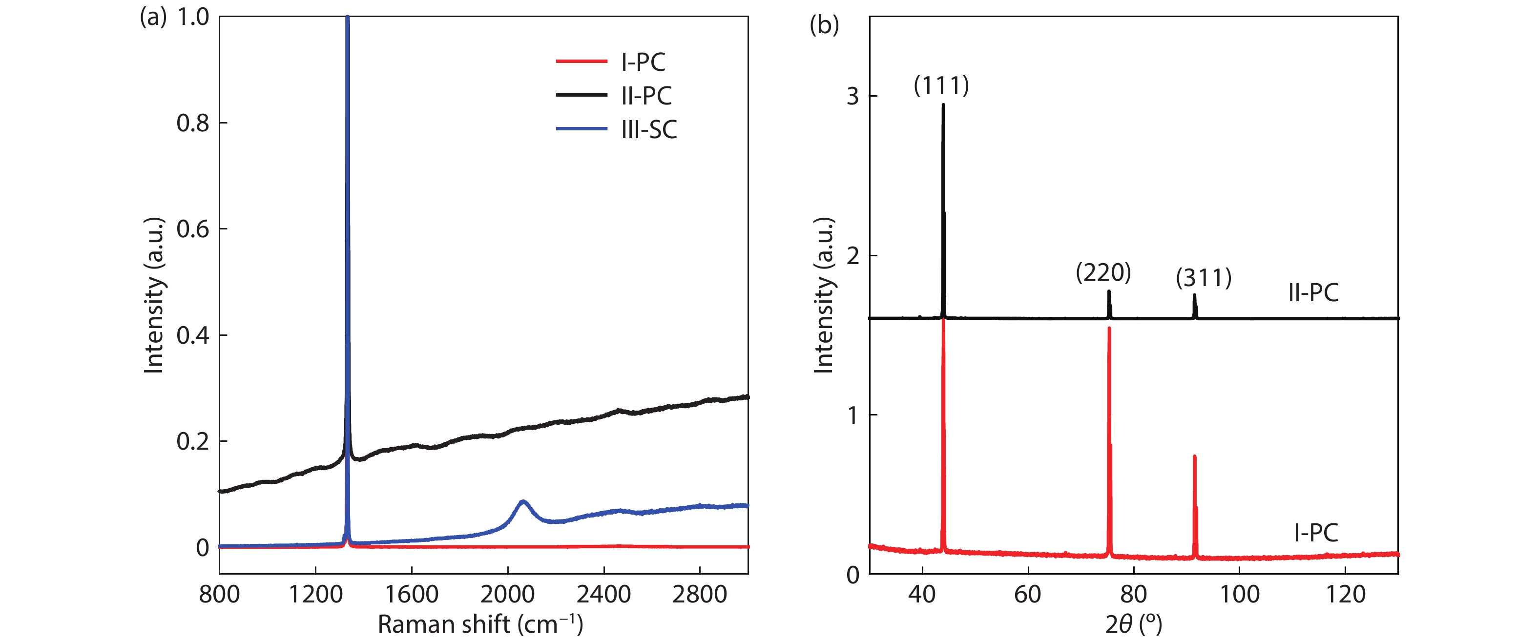
Fig. 1 shows the Raman spectra and XRD pattern of the three diamond samples. It can be seen that the background of the sample I-PC is very small. But for the samples II-PC and III-SC, the background line shows a significant upward movement, which is proven to be due to the increase of defect and impurity content[
![]()
Figure 1.(Color online) (a) Raman spectra of the I-PC, II-PC, and III-SC diamond samples. (b) XRD pattern of I-PC, and II-PC diamond samples.
The gate length and source–drain space of the three diamond samples were shown in Table 1[
Pulsed I–V characteristics for the III-SC sample at different quiescent bias points were measured, as shown in Fig. 2. The measured results for the I-PC and II-PC samples have been shown in our previous work[
![]()
Figure 2.(Color online) Pulsed
The small signal S-parameters of the diamond FETs were measured between 0.1–30 GHz[
![]()
Figure 3.(Color online) Relationship of cutoff frequency
The component parameters of the three diamond samples extracted from the small single parameters are shown in Table 2. The three samples show comparable cut-off frequency fT, but fmax values show big difference. The extrinsic fmax for transistors can be expressed as[
It can be seen that the parasitic resistance has strong influence on the extrinsic fmax for transistors. The fmax value of sample II-PC is the lowest. This is due to its rectangular gate structure, which makes the gate resistance Rg large, as shown in Table 2.
Fig. 4 shows the RF power output characteristic measured at 2 GHz under a continuous-wave signal (A-class) for the I-PC diamond FET. As shown in the figure, the maximum gain is 18.3 dB and the power added efficiency (PAE) is 22.9%. The maximum output power density (Pout) reaches 877 mW/mm at 2 GHz for our diamond FET. It is the best reported output power density for diamond FETs measured at 2 GHz[
![]()
Figure 4.(Color online) Large signal performance of I-PC diamond FET at 2 GHz power sweep (A-class).
where Ids-max is the maximum drain current density, Vwork is the drain voltage for the measurement of Pout, and Vknee is the knee voltage. The large-signal power gain result shows that the device exhibits a large compression even at class-A operation. The possible reasons are that the drain current density (323 mA/mm) is small, and the knee voltage (~6 V) is high for the H-terminated diamond FETs. The sheet resistance of the H-terminated diamond is high (~kΩ/□), and the parasitic resistance is high (poor Ohmic contact). Table 3 shows the compare of measured output power density and calculated output power density for the three diamond samples (I-PC, II-PC, and III-PC). The drain voltage values for the measurements of the three samples are –25, –24, and –25 V, respectively. It can be seen that for all three samples, the measured output power densities are lower than the calculated output power densities, which should be due to the trapping effects. The knee voltage will increase at continuous drain voltage and the drain current will degrade. Both of them would cause a decrease in output power. The II-PC sample shows the largest degrade in output power density. This is consistent with the pulsed I–V measurement. This sample shows the largest maximum drain current degeneration induced by drain-lag effect. These results indicate that defects and N impurities in the diamond act as traps in the carrier transport and have great influence on the output power characteristics of diamond FETs.
4. Conclusion
In summary, three kinds of diamond FETs were fabricated on polycrystalline and single crystal hydrogen-terminated diamond with different defect levels and impurity contents. Direct current and radio frequency performances analysis show that the frequency of devices depends mainly on the parasitic parameters, which are closely related to the device structure. Meanwhile, the output power density is greatly influence by the defect and impurity level of the samples. The defects and impurities in the diamond act as traps in the carrier transport. The trapping effects induce the knee voltage increase and the drain current degrade at continuous drain voltage. Diamond with high crystal quality and low impurity level is in great demand for microwave power devices.
Acknowledgements
This work was supported by the National Natural Science Foundation of China (Grant No. 51702296), and Excellent Youth Foundation of Hebei Scientific Committee (Grant No. F2019516002).
References
[1] C J H Wort, R S Balmer. Diamond as an electronic material. Mater Today, 11, 22(2008).
[2] K Hirama, H Sato, Y Harada et al. Thermally stable operation of H-terminated diamond FETs by NO2 adsorption and Al2O3 passivation. IEEE Electron Device Lett, 33, 1111(2012).
[3] K Ueda, M Kasu, Y Yamauchi et al. Diamond FET using high-quality polycrystalline diamond with
[4] S Imanishi, K Horikawa, N Oi et al. 3.8 W/mm RF power density for ALD Al2O3-based two-dimensional hole gas diamond MOSFET operating at saturation velocity. IEEE Electron Device Lett, 40, 279(2018).
[5]
[6]
[7] J J Wang, Z Z He, C Yu et al. Comparison of field-effect transistors on polycrystalline and single-crystal diamonds. Diamond Relat Mater, 70, 114(2016).
[8]
[9] S D Woltera, J T Praterb, Z Sitara. Raman spectroscopic characterization of diamond films grown in a low-pressure flat flame. J Cryst Growth, 226, 88(2001).
[10] C J Zhou, J J Wang, J C Guo et al. Radio frequency performance of hydrogenated diamond MOSFETs with alumina. Appl Phys Lett, 114, 063501(2019).
[11] C Yu, C J Zhou, J C Guo et al. 650 mW/mm output power density of H-terminated polycrystalline diamond MISFET at 10 GHz. Electron Lett, 56, 334(2020).
[12] H Sato, M Kasu. Maximum hole concentration for Hydrogen-terminated diamond surfaces with various surface orientations obtained by exposure to highly concentrated NO2. Diamond Relat Mater, 31, 47(2013).
[13] S Yamanaka, D Takeuchi, H Watanabe et al. Low-compensated boron-doped homoepitaxial diamond films using trimethylboron. Phys Status Solidi A, 174, 59(1999).
[14] K Hirama, K Tuge, S Sato et al. High performance p-channel diamond metal-oxide-semiconductor field-effect transistors on H-terminated (111) surface. Appl Phys Express, 3, 044001(2010).
[15] S A O Russell, S Sharabi, A Tallaire et al. Hydrogen-terminated diamond field-effect transistors with cutoff frequency of 53 GHz. IEEE Electron Device Lett, 33, 1471(2012).
[16] K Hirama, H Takayanagi, S Yamauchi et al. High-performance p-channel diamond MOSFETs with alumina gate insulator. IEDM Tech Dig, 873(2007).
[17] V Camarchia, F Cappelluti, G Ghione et al. RF power performance evaluation of surface channel diamond MESFETs. Solid-State Electron, 55, 19(2011).
[18] X X Yu, C J Zhou, C J Qi et al. A high frequency hydrogen-terminated diamond MISFET With
[19] P J Tasker, B Hughes. Importance of source and drain resistance to the maximum
[20] T G Ivanov, J Wei, P B Shah et al. Diamond RF transistor technology with

Set citation alerts for the article
Please enter your email address
© Copyright 2018-2021 | Chinese Laser Press. All Rights Reserved 沪ICP备15018463号-20