
Zejie Yu, He Gao, Yi Wang, Yue Yu, Hon Ki Tsang, Xiankai Sun, Daoxin Dai. Fundamentals and applications of photonic waveguides with bound states in the continuum[J]. Journal of Semiconductors, 2023, 44(10): 101301
- Journal of Semiconductors
- Vol. 44, Issue 10, 101301 (2023)
![(Color online) (a) Strip, slot, ridge, and subwavelength waveguides. (b) A plasmonic slot waveguide. (c) A hybrid waveguide[18]. Copyright 2016, The Optical Society. (d) A photonic crystal waveguide. (e) A hybrid plasmonic cap waveguide[28]. Copyright 2009, The Optical Society.](/richHtml/jos/2023/44/10/101301/jos_44_10_101301_f1.jpg)
Fig. 1. (Color online) (a) Strip, slot, ridge, and subwavelength waveguides. (b) A plasmonic slot waveguide. (c) A hybrid waveguide[18]. Copyright 2016, The Optical Society. (d) A photonic crystal waveguide. (e) A hybrid plasmonic cap waveguide[28]. Copyright 2009, The Optical Society.
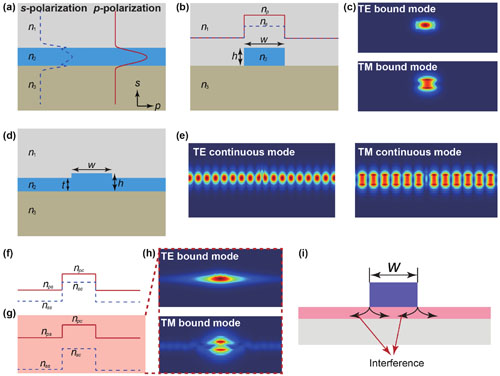
Fig. 2. (Color online) (a) A slab waveguide and its s- and p-polarized modal profiles. (b) A strip waveguide with its RI distributions of both s and p polarizations. (c) Modal profiles |E | of the TE and TM modes in a strip waveguide. (d) A ridge waveguide. (e) Modal profiles |E | of TE and TM continuous modes. The RI distributions of the ridge waveguide with nsc > nps (f) and nsc < nps (g). (h) Modal profiles of the TE and TM modes in a thin-ridge waveguide with nsc < nps. (i) Schematically illustration of leakage channels.
Fig. 3. (Color online) (a) Schematically illustration of a thin-ridge silicon waveguide. (b) The propagation loss of the TM mode as a function of the waveguide width[72]. Copyright 2009, IEEE. (c) Modal profiles of the TM mode at waveguides with “magic width” and “anti-magic width”[72]. Copyright 2009, IEEE. (d) Planar view and modal coupling diagram of a bend thin-ridge waveguide[81]. Copyright 2010, The Optical Society. (e) The propagation loss of the TM mode in a bent waveguide as a function of the waveguide width and radius[81]. Copyright 2010, The Optical Society.
Fig. 4. (Color online) (a) A fabricated silicon thin-ridge waveguide and the scattering field views of waveguides with “magic width” and “non-magic width”[66]. Copyright 2016, IEEE. (b) The measured propagation loss of the waveguide with different widths[66]. Copyright 2016, IEEE. (c) Modal profiles of the TE and TM modes in a waveguide with “anti-magic” structural parameters[82]. Copyright 2010, The Optical Society. (d) The measured results for the transmissions of the TE and TM modes[82]. Copyright 2010, The Optical Society.
Fig. 5. (Color online) (a) Schematic illustration of a silicon thin-ridge waveguide supporting BIC resonances and its simulated transmission spectra as a function of waveguide width and incident angle[77]. Copyright 2018, Chinese Laser Press. (b) A fabricated silicon waveguide supporting BIC resonances and its measured resonance[76]. Copyright 2019, John Wiley & Sons. (c) A fabricated metagrating waveguide and its measured BIC resonance for applications in sensing[83]. Copyright 2020, John Wiley & Sons. (d) A flat-top filter based on BIC waveguides and its simulated transmission and reflection spectra[60]. Copyright 2019, Chinese Laser Press.
Fig. 6. (Color online) (a) Schematic illustration of a straight hybrid waveguide[56]. (b) RI distributions of s and p polarizations. (c) Modal profiles of a TM mode in waveguides with BIC and non-BIC parameters[56]. (d) Fabricated straight waveguides and measured propagation loss as a function of waveguide width[56]. (e) Fabricated bent waveguides and measured propagation loss as functions of waveguide width and bending radius[56]. Copyright 2019, The Optical Society.
Fig. 7. (Color online) (a) Measured transmission spectrum of the fabricated microring cavity with structural parameters satisfying the BIC condition[56]. (b) Optical microscope image of the fabricated directional coupler and the corresponding measured spectrum[56]. (c) Optical microscope image of the fabricated MZI and the corresponding measured spectrum[56]. Copyright 2019, The Optical Society.
Fig. 8. (Color online) (a) An optical microscope image of the fabricated mode (de)multiplexer integrated with EO modulators[55]. (b) Propagation loss and effective RIs of the different orders of TM modes as a function of the waveguide width w[55]. (c) Normalized spectra of light transmission for a fabricated mode (de)multiplexer[55]. (d) Measured modulated signals for each order of modes[55]. Copyright 2020, Springer Nature Limited.
Fig. 9. (Color online) (a) Schematic illustration of AO cavity modulation[59]. (b) Measured AO modulation signals with a frequency higher than 4 GHz[59]. (c) Measured AO-induced transparency and absorption[59]. Copyright 2020, Light: Science & Applications. (d) Schematic illustration of AO waveguide modulation[61]. (e) Measured frequency shifts[61]. Copyright 2021, ACS.
Fig. 10. (Color online) (a) Schematic illustration of a 2D material integrated with a BIC waveguide[63]. (b) A fabricated hybrid graphene thermo-optic modulator with BICs and its measured spectra[63]. (c) A fabricated hybrid graphene photodetector with BICs and its measured optoelectrical response[63]. (d) A fabricated hybrid graphene EO modulation with BIC and its measured EO response[63]. Copyright 2019, John Wiley & Sons. (e) A fabricated hybrid PtSe2 photodetector with BICs and its measured optoelectrical response[62]. Copyright 2020, ACS.

Set citation alerts for the article
Please enter your email address
© Copyright 2018-2021 | Chinese Laser Press. All Rights Reserved 沪ICP备15018463号-20