1Centre for Optical and Electromagnetic Research, State Key Laboratory for Modern Optical Instrumentation, Zhejiang Provincial Key Laboratory for Sensing Technologies, International Research Center for Advanced Photonics, College of Optical Science and Engineering, Zhejiang University, Hangzhou 310058, China
2Department of Electronic Engineering, The Chinese University of Hong Kong, Shatin, New Territories, Hong Kong SAR, China
3Jiaxing Key Laboratory of Photonic Sensing & Intelligent Imaging, Jiaxing 314000, China
4Intelligent Optics & Photonics Research Center, Jiaxing Research Institute Zhejiang University, Jiaxing 314000, China
5Ningbo Research Institute, Zhejiang University, Ningbo 315100, China
Zejie Yu, He Gao, Yi Wang, Yue Yu, Hon Ki Tsang, Xiankai Sun, Daoxin Dai. Fundamentals and applications of photonic waveguides with bound states in the continuum[J]. Journal of Semiconductors, 2023, 44(10): 101301
Copy Citation Text
Photonic waveguides are the most fundamental element for photonic integrated circuits (PICs). Waveguide properties, such as propagation loss, modal areas, nonlinear coefficients, etc., directly determine the functionalities and performance of PICs. Recently, the emerging waveguides with bound states in the continuum (BICs) have opened new opportunities for PICs because of their special properties in resonance and radiation. Here, we review the recent progress of PICs composed of waveguides with BICs. First, fundamentals including background physics and design rules of a BIC-based waveguide will be introduced. Next, two types of BIC-based waveguide structures, including shallowly etched dielectric and hybrid waveguides, will be presented. Lastly, the challenges and opportunities of PICs with BICs will be discussed.
Photonic integrated circuits (PICs) can enable systems to operate with a large bandwidth, high speed, low power consumption, and high thermal stability, and have the potential to revolutionize the future technologies used in multidisciplinary areas such as high-speed communication[1, 2], energy-efficient computating[3, 4], quantum information processing and communications[5, 6], and precise metrology[7, 8]. Integrated optical waveguides are the fundamental element for constructing PICs, and are of critical importance. Key characteristics of a waveguide include their effective refractive index (RI), RI contrast between the guide and cladding regions, waveguide sidewall roughness, waveguide feature size, nonlinear coefficients, loss, and optical dispersion and these directly influence the performance and functionalities in PICs. For example, the high integration density of PICs requires the use of waveguides with high RI and high RI contrast to realize small modal areas, weak coupling between closely positioned adjacent waveguides, and a small bending radius. Waveguides with low propagation losses are often a key requirement for high-performance PICs and are an essential prerequisite for the integration of a large number of devices on a chip. Strong light‒matter interaction in applications of optical emission[9−12], detection[13, 14], and wavelength conversion[15−17] require waveguides with large nonlinear coefficients, small modal areas, low loss, etc.
A variety of waveguides, as shown in Fig. 1, have been widely explored in different material platforms[19−22]. A strip waveguide is the most popular waveguide with characteristics such as simple structures, small modal area, large RI contrast, etc. Although the strip waveguide offers high performance for most applications, there are some circumstances when other waveguide structures are needed. For example, a ridge waveguide can have a smaller optical field overlap with the shallowly etched sidewalls than strip waveguides, thus achieving lower propagation loss. Subwavelength grating structures can be used for waveguides and offer an additional degree of freedom for engineering the effective RI, birefringence, and dispersion, and may be used to design devices with wider working bandwidths[23]. Photonic crystal waveguides with engineered band diagrams could realize unusual phenomena such as sharp bending[24], slow light[25], and topological protection[26]. Plasmonic waveguides confining light into the deep subwavelength region is a good platform to study nonlinear light‒matter interactions[27, 28]. Hybrid waveguides integrating different materials can realize active and passive devices on a single chip[18, 29].
Figure 1.(Color online) (a) Strip, slot, ridge, and subwavelength waveguides. (b) A plasmonic slot waveguide. (c) A hybrid waveguide[18]. Copyright 2016, The Optical Society. (d) A photonic crystal waveguide. (e) A hybrid plasmonic cap waveguide[28]. Copyright 2009, The Optical Society.
Bound states in the continuum (BICs) were first mathematically proposed in 1929 by von Neumann and Wigner[30]. Solved from the Schrödinger equation, a typical potential well only supports a wave with eigenenergy below the potential well, and the wave is called a bound state of the potential well. Other states with eigenenergy above the potential well are known as continuous states, which cannot be effectively confined and will spread to infinity. A bound state with eigenenergy above the potential well will suffer large leakage loss because of the interaction with radiation waves. BIC is just an exception that has eigenenergy above the potential well but is perfectly confined in the continuous spectrum without any loss. Even though the original proposal constructing an artificial quantum well to support an electronic state with energy that falls above the continuum threshold was never practically realized[31], BICs are a general wave phenomenon that can be explored in other systems such as electromagnetic[32−45] and acoustic[46−50] waves. For example, BICs can be obtained in photonics using the similarity between the Schrödinger equation and the Helmholtz equation, the refractive index n of a material determines the potential for photons as −n2k20, where k0 is the light’s wavenumber in the vacuum. Recently, photonics become a hot platform to explore the background physics of BICs because of the advancement of micro/nano-fabrication technology. Different types of BICs have been observed in different kinds of photonic structures including supercavities[43], photonic crystals[51], metasurface[52, 53], photonic waveguide arrays[44, 54], hybrid waveguides[55, 56], plasmonic metagrating[57], etc.
Among the different kinds of waveguides in Fig. 1, most of them only support optical modes that do not couple with leakage modes. The supported mode is recognized as a bound mode of the corresponding waveguide. In recent years, a new type of waveguide supporting BICs gradually attract attention due to their special optical properties. Optical modes belonging to the category of BICs in waveguides can propagate without any leakage loss even though they coexist and couple with leaky continuous modes[56, 58]. The waveguide with BICs has brought new chances to PICs and many applications have been demonstrated such as cavities[56, 58, 59], filters[60], modulations[55, 59, 61], and detections[62, 63]. In this paper, a review is given of the recent progress of waveguides with BICs, and fundamentals, applications, challenges, and opportunities will be introduced.
Fundamentals of a waveguide with BICs
Generally, modal profiles, propagation loss, and propagation speed (inversely proportional to group RI) are three crux features to characterize light properties in a waveguide. A slab waveguide as shown in Fig. 2(a) consists of three layers of materials with RIs of n1, n2, and n3, respectively, where n2 is larger than both n1 and n3. All RIs n1, n2, and n3 are assumed to be real numbers because negligible material absorption is highly desired for PIC applications. The optical properties of a passive waveguide can be solved by the passive Helmholtz equation as
Figure 2.(Color online) (a) A slab waveguide and its s- and p-polarized modal profiles. (b) A strip waveguide with its RI distributions of both s and p polarizations. (c) Modal profiles |E| of the TE and TM modes in a strip waveguide. (d) A ridge waveguide. (e) Modal profiles |E| of TE and TM continuous modes. The RI distributions of the ridge waveguide with nsc > nps (f) and nsc < nps (g). (h) Modal profiles of the TE and TM modes in a thin-ridge waveguide with nsc < nps. (i) Schematically illustration of leakage channels.
where n and c denote the RI of the material and light speed in the vacuum, respectively. Solved modal profiles for both polarizations are plotted as solid (p-polarization) and dashed (s-polarization) lines in Fig. 2(a), where s polarization with the electrical field perpendicular to the interface of two materials has an effective RI of ns and p polarization with the electrical field parallel to the interface of two materials has an effective RI of np. np is usually larger than ns because the higher RI material concentrates more p-polarized light than s-polarized light. The propagation loss of both s- and p-polarized light can be neglected by assuming zero roughness at the interface of two materials.
A strip waveguide as shown in Fig. 2(b) is more practical than a slab waveguide in real applications. In order to solve the optical properties of the strip waveguide, it can be divided into three regions and the central region can be approximated as a slab waveguide. In the side regions, the effective RI of both s- and p-polarized light can be approximated as n1. In terms of the central region, as discussed for the slab waveguide, the effective RIs of s- and p-polarized light can be approximated as ns and np, respectively. The solid (p-polarized) and dashed (s-polarized) lines in Fig. 2(b) plot the effective RI distributions for s- and p-polarized light, respectively. It should be noted that only the TE (TM) mode can be solved from the p(s)-polarized effective-RI distribution because the polarization of light has been assumed when plotting the effective RI distributions. Fig. 2(c) shows the solved modal profiles |E| of the TE and TM modes, where the TE mode usually has a larger effective RI than that of the TM mode because the width w of the waveguide usually is larger than the height h.
Fig. 2(d) shows a ridge waveguide with shallowly etched sidewalls. Like a strip waveguide, it can also be divided into three regions to solve the optical properties. Each region of the ridge waveguide can be seen as a slab waveguide. The central and side regions have effective RIs of nsc (npc) and nss (nps) for s(p)-polarized light, where nsc (nss) < npc (nps) and nsc (npc) > nss (nps). Regarding modal properties in the ridge waveguide, at first, there are many TE (TM) continuous modes with effective RIs smaller than np(ns) existing in the slab as shown in Fig. 2(e). These modes extend to the infinite in the lateral direction of the waveguide so that suffer large leakage loss. In terms of the guided modes, the TE and TM modes with effective RIs of nTE and nTM can be obtained, where nps < nTE < npc and nss < nTM < nsc as analyzed above. In view of that, the effective RI of s-polarized light at the side regions will decrease with the etching depth, so the TE and TM modal evolution mechanism in the ridge waveguide can be divided into two cases according to the relative value between nsc and nps. Fig. 2(f) plots the effective RIs distributions of the ridge waveguide with nsc > nps, which is similar to the condition of the strip waveguide. Fig. 2(g) plots the case of nsc < nps, which indicates that the RI distribution of s-polarized light is below the RI distribution of p-polarized light. Given the fact that the RI contrast for the TE polarization is quite small in a thin-ridge waveguide, the TE mode (Fig. 2(h)) has a weak confinement that is not suitable for constructing compact integrated devices. In addition, despite s-polarization has a relatively large RI contrast because the discontinuities of the electric field at the up and down boundaries make s-polarization more sensitive to the waveguide thickness, the TM mode falls in the TE continuous spectrum so that a TE continuous mode with the same effective RI as nTM can be found. Considering the TM mode in the ridge waveguide actually is a quasi-TM mode that contains both s and p polarizations, the TM mode as shown in Fig. 2(h) will couple with the leaky TE continuous modes so that suffers large propagation loss.
Obtaining a BIC is a solution to overcome the leakage loss of the TM mode in the TE continuous spectrum if taking the thin-ridge waveguide into PIC applications. As shown in Fig. 2(i), the leakage channels of the TM bound mode in the ridge waveguide are at the corners and at each corner both left- and right-going leakages exist. Leakages with the same direction will interfere with each other and effective leakage can be reduced to zero when destructive interferences happen, enabling zero propagation loss for the TM mode. For a straight waveguide, the interference can be simply controlled by changing the width of the ridge waveguide, the propagation length can be expressed as L∝w2/sin2(kpw/2)[58], with kp the p component of the wave vector of the TE continuous mode. For a bent waveguide, the interference depends on both waveguide width w and bending radius R, the propagation loss can be briefly expressed as ∝|Jq(nk0R) − ξJq(nk0(R − wb))|[58], where Jq is the qth Bessel function with q the azimuthal mode number. The waveguide with parameters supporting negligible propagation loss can be called a BIC waveguide and the corresponding guided TM mode is a BIC.
Silicon waveguides with BICs
Silicon ridge waveguides with BICs have been widely and thoroughly investigated on a silicon-on-insulator platform[64−80]. According to the propagation direction of light, the working mechanism of BICs can be categorized into two types: one is that light propagates along a silicon ridge waveguide and the other is that light propagates with a certain angle between a silicon ridge waveguide.
Light propagating along a silicon thin-ridge waveguide. A shallowly etched waveguide on an SOI platform as shown in Fig. 3(a) is a typical platform to study the case of light propagating along a silicon thin-ridge waveguide. Despite semi-analytical mode-matching methods have been developed to solve the leakage behavior of the TM mode[72], numerical simulation is the most widely adopted method to accurately analyze leakage by solving eigenmodes in the waveguide cross section, where the propagation loss can be evaluated from the imaginary part of the solved eigenmodal effective RI. The finite element method with absorption boundaries e.g., perfectly matched layer boundaries is a typical approach to obtain effective RIs. The simulated leakage loss of the TM mode as a function of the waveguide width is presented in Fig. 3(b), where the propagation loss of the TM mode varies periodically with the waveguide width. These special widths for minimum or maximum propagation loss were called “magic widths” or “anti-magic widths”. Moreover, the TM mode at the waveguide with magic or anti-magic width can be recognized as a BIC or anti-BIC. Fig. 3(c) shows vectorial components of the electric field distributions of the guided modes for a waveguide with “magic width” and “non-magic width”, respectively. Comparing the components, despite the s-polarized components being effectively confined by the thin-ridge waveguide, a significant p-polarized component with field values approximately ten times smaller than the s-polarized component exhibits strong radiation at the waveguide with a “non-magic” width. The leakage behavior was also explored in a bent thin-ridge waveguide[81] as shown in Fig. 3(d). The simulated results in Fig. 3(e) reveal that the propagation loss is sensitive to both waveguide radius and width, the interplay between waveguide radius and width is nontrivial. The lateral leakage can be significantly reduced with “magic parameters” but cannot be reduced to zero due to the impact of the conventional bending loss.
Figure 3.(Color online) (a) Schematically illustration of a thin-ridge silicon waveguide. (b) The propagation loss of the TM mode as a function of the waveguide width[72]. Copyright 2009, IEEE. (c) Modal profiles of the TM mode at waveguides with “magic width” and “anti-magic width”[72]. Copyright 2009, IEEE. (d) Planar view and modal coupling diagram of a bend thin-ridge waveguide[81]. Copyright 2010, The Optical Society. (e) The propagation loss of the TM mode in a bent waveguide as a function of the waveguide width and radius[81]. Copyright 2010, The Optical Society.
The lateral leakage behaviors in a ridge waveguide were experimentally investigated on an SOI platform[66]. The lateral leakage was proved by scattering radiated light into free space with the assistance of side gratings as shown in Fig. 4(a). The waveguide with a “magic width” has an image with darkness, presenting clear evidence of the suppression of lateral leakage, while the waveguide with a “non-magic width” has an image with excitation decreasing with distance from the input, presenting clear evidence of lateral leakage behavior in the ridge. Fig. 4(b) shows the propagation loss as a function of waveguide width at the wavelength of 1550 nm, indicating the minimum propagation loss of 0.357 dB/mm.
Figure 4.(Color online) (a) A fabricated silicon thin-ridge waveguide and the scattering field views of waveguides with “magic width” and “non-magic width”[66]. Copyright 2016, IEEE. (b) The measured propagation loss of the waveguide with different widths[66]. Copyright 2016, IEEE. (c) Modal profiles of the TE and TM modes in a waveguide with “anti-magic” structural parameters[82]. Copyright 2010, The Optical Society. (d) The measured results for the transmissions of the TE and TM modes[82]. Copyright 2010, The Optical Society.
A simple and broadband polarizer as shown in Fig. 4(c) was proposed based on the distinct propagation loss between the TE and TM modes of a thin-ridge waveguide on an SOI platform[82]. The theoretical calculation shows that the loss of the TE mode can be very low while at the same time the TM mode has a very large leakage loss when the waveguide with an “anti-magic” width. The polarizer is fabricated on an SOI wafer with a 700-nm-thick top layer silicon and then characterized by using a free-space optical system. As shown in Fig. 4(d), the measured extinction ratio is as high as 25 dB over a 100 nm wavelength range for a 1-mm-long polarizer.
Angled propagation across a silicon thin-ridge waveguide. According to the BIC formation mechanism of coupling between the TE continuous and TM modes, similar to the condition that TM mode propagating in a ridge waveguide, photonic BICs can also be explored when TE continuous modes incident on a silicon thin-ridge waveguide with a certain angle as shown in Fig. 5(a)[77]. Under the oblique incidence of a p-polarized light on the thin-ridge waveguide, BICs can be observed at the reflectance and transmittance spectra, featured as high-Q resonances. The BICs or resonances highly depend on the incident angle and waveguide width because of the phase-matching requirement of coupling. A theoretical model was developed to explain these optical properties based on the coupled-mode method, not only proving the existence of BICs but also predicting their corresponding locations[77]. The accuracy of the theoretical model was verified by the aperiodic rigorous coupled-wave analysis method. The phenomenon was experimentally observed based on an SOI platform as shown in Fig. 5(b) using the foundry-compatible fabrication process[76]. A single-mode waveguide launches a slab waveguide mode by adiabatically expanding the width. The slab mode is collimated by a parabolic reflector and then propagates to a 650-nm-wide ridge resonator under an angle of 52.2°. The transmitted light is focused into the right single-mode waveguide by another parabolic reflector. A single and strong resonant dip is observed at the wavelength of 1539 nm with a Q factor of 520.
Figure 5.(Color online) (a) Schematic illustration of a silicon thin-ridge waveguide supporting BIC resonances and its simulated transmission spectra as a function of waveguide width and incident angle[77]. Copyright 2018, Chinese Laser Press. (b) A fabricated silicon waveguide supporting BIC resonances and its measured resonance[76]. Copyright 2019, John Wiley & Sons. (c) A fabricated metagrating waveguide and its measured BIC resonance for applications in sensing[83]. Copyright 2020, John Wiley & Sons. (d) A flat-top filter based on BIC waveguides and its simulated transmission and reflection spectra[60]. Copyright 2019, Chinese Laser Press.
The BIC-enabled ridge resonance has also been observed in a metagrating-assisted waveguide as shown in Fig. 5(c)[83], where the launched TE continuous mode is perpendicular with the ridge waveguide. By satisfying the phase-matching condition through the assistance of shallow-ridge metagrating embedded in the silicon slab waveguide, the input slab mode can be coupled into the resonant TM mode, which can be further transformed into the supercavity mode by utilizing the intra-waveguide Fabry–Perot interference. The fabricated metagrating operating near the supercavity regime with an experimentally observed high-quality factor ≈ 5200 proved the existence of the BIC. As an application, such a high-quality metagrating is exploited to realize the temperature sensing with a high-temperature sensitivity ≈ 77 pm/K.
A narrowband integrated flat-top filter was proposed by utilizing identical coupled thin-ridge waveguides as shown in Fig. 5(d)[60]. These thin-ridge waveguides operating near a BIC work as a coupled-resonator array for p-polarized guided modes, enabling sidelobe-free and flat-top reflectance profiles with steep slopes. Particularly, a two-ridge structure can be seen as a second-order Butterworth filter and an excellent higher-order Butterworth filter can be realized by increasing the number of thin-ridge waveguides. The flat-top reflection band can be an arbitrary value by proper choice of the linewidth of a single-ridge resonance and coupling strength between neighboring ridges. In addition, the linewidth of a single ridge and coupling strength between neighboring ridges can be simply controlled by the width of the ridge and the distance between neighboring ridges.
Hybrid waveguides with BICs
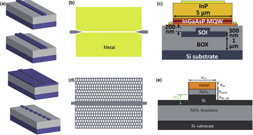
Up to now, many excellent materials have been adopted for photonic integration such as silicon, silicon nitride, alumina nitride, lithium niobite (LiNbO3), etc. However, many other materials with excellent properties cannot be utilized due to the lack of high-quality etching. Ordinarily, the material etching process involves chemical reactions so different kinds of materials need to develop different kinds of etching recipes. Therefore, a general method for overcoming the etching challenges of different kinds of materials is highly desired. As shown in Fig. 6(a), a hybrid waveguide with an etching-friendly waveguide atop an etching-challenging dielectric material is a common structure to overcome the etching problem. In order to fully make use of the excellent properties of the dielectric material, the etching-friendly waveguide should have a lower RI than that of the etching-challenging dielectric material so that light can be mainly confined in the dielectric material. However, in this condition, the waveguide is very similar to the case of a ridge waveguide with nsc < nps, e.g., a s-polarized RI distribution well is below a TE RI distribution well. Therefore, a TM mode in the TE continuous spectrum should be obtained, then the etching challenge can be solved for different kinds of dielectric materials.
Figure 6.(Color online) (a) Schematic illustration of a straight hybrid waveguide[56]. (b) RI distributions of s and p polarizations. (c) Modal profiles of a TM mode in waveguides with BIC and non-BIC parameters[56]. (d) Fabricated straight waveguides and measured propagation loss as a function of waveguide width[56]. (e) Fabricated bent waveguides and measured propagation loss as functions of waveguide width and bending radius[56]. Copyright 2019, The Optical Society.
The hybrid waveguide with BICs was first proposed and demonstrated by utilizing a low RI polymer waveguide on a high RI LiNbO3 substrate[56]. Fig. 6(b) plots the RI distributions of a hybrid waveguide with the thicknesses of the LiNbO3 layer of 300 nm at a wavelength of 1550 nm. The modal profiles of the TM modes in waveguides with BIC and non-BIC parameters are shown in Fig. 6(c). Fig 6(d) plots the propagation loss of a straight waveguide as a function of waveguide width, indicating the low-loss TM mode can be obtained by optimizing the waveguide width to BIC parameters. As for a bent waveguide, the propagation loss depends on both the waveguide width and bending radius as shown in Fig. 6(e).
Pivotal photonic components have been demonstrated[56] based on the basic straight and bent waveguides including microcavities, directional couplers, and Mach–Zehnder interferometers (MZIs). The measured transmission spectrum of a microring cavity as shown in Fig. 7(a) indicates that the demonstrated microcavities can support high-Q resonances with high extinction ratio over a broad bandwidth of 100 nm. The loaded and intrinsic Q factors can reach 2.2 × 10⁵ and 5.8 × 10⁵, respectively. The transmission spectra of a fabricated directional coupler as shown in Fig. 7(b) indicate that light can efficiently be coupled from one port to another in the wavelength range of 1450–1600 nm. The measured spectra of the fabricated MZI as shown in Fig. 7(c) has a large extinction ratio, denoting the 3-dB power splitters divide optical power evenly. Moreover, the hybrid waveguide with BICs has also been demonstrated at near-visible wavelength spectrum[84] based on a structure with the thicknesses of the LiNbO3 layer, the buried silicon oxide underneath, and the organic polymer atop are 150 nm, 2 μm, and 500 nm, respectively.
Figure 7.(Color online) (a) Measured transmission spectrum of the fabricated microring cavity with structural parameters satisfying the BIC condition[56]. (b) Optical microscope image of the fabricated directional coupler and the corresponding measured spectrum[56]. (c) Optical microscope image of the fabricated MZI and the corresponding measured spectrum[56]. Copyright 2019, The Optical Society.
Mode (de)multiplexing. Mode (de)multiplexing is an important freedom among different kinds of (de)multiplexing technologies, which can greatly increase data link capacity to satisfy the huge data transmission requirement. Mode (de)multiplexing and high-dimensional communication were achieved on a LiNbO3 platform utilizing waveguides with BICs as shown in Fig. 8(a)[55], which is composed of several cascaded multimode directional couplers. Fig. 8(b) plots the effective RI and propagation loss of the TM0 (orange), TM1 (blue), TM2 (red), and TM3 (green) modes as a function of the waveguide width w, indicating the waveguides can be engineered to meet low propagation loss and phase-matching conditions simultaneously. Specifically, the gray areas denote the regions of low propagation loss for the corresponding modes and satisfaction of phase matching can be realized at the intersections of the horizontal solid line and the dashed lines in the gray regions. Fig. 8(c) shows the measured transmission spectra of all pairs of input-output ports. The measured insertion loss (crosstalk) can be <1.7(−14.1), <3.4(−13.8), <4.0(−15.7), and <3.3(−18.5) dB for the TM0, TM1, TM2, and TM3 modes, respectively, within a wavelength spectrum of 1.51–1.58 μm. Therefore, a hybrid mode–wavelength (de)multiplexing optical network can be constructed to significantly increase optical link capacity based on the wideband mode (de)multiplexer. Furthermore, the capability of on-chip electro-optic (EO) modulation and mode (de)multiplexing simultaneously was evidenced by integrating EO modulators with the mode (de)multiplexer on the same chip. Fig. 8(d) plots the transmission signal for the input and output pairs of TM0–TM0, TM1–TM1, TM2–TM2, and TM3–TM3, respectively.
Figure 8.(Color online) (a) An optical microscope image of the fabricated mode (de)multiplexer integrated with EO modulators[55]. (b) Propagation loss and effective RIs of the different orders of TM modes as a function of the waveguide width w[55]. (c) Normalized spectra of light transmission for a fabricated mode (de)multiplexer[55]. (d) Measured modulated signals for each order of modes[55]. Copyright 2020, Springer Nature Limited.
AO modulation. AOs explore phonon–photon coupling based on strain- and stress-induced RI variation in a medium. Brillouin scattering involving the study of propagating phonons is one of the most widely investigated AO effects, which can break the time-reversal and frequency-modulation symmetry of light due to the phase-matching requirement. It has found wide applications in various areas, such as nonreciprocal light transmission[85], modulation[86], frequency shifting[87, 88], and signal processing[89, 90]. AO cavity and waveguide modulations have been demonstrated based on the hybrid waveguides with BICs.
AO cavity modulation has been realized as shown in Fig. 9(a)[59], where a surface acoustic wave (SAW) interdigital transducer (IDT) is monolithically integrated with a photonic microcavity that supports BIC modes on a 400-nm-LiNbO3-on-insulator platform. A SAW will propagate across a BIC waveguide smoothly because the polymer waveguide atop with very different acoustic properties from those of LiNbO3 has a negligible effect on the SAW propagating inside the LiNbO3 thin film. AO modulation with frequency >4 GHz was observed as shown in Fig. 9(b) because of the microscale confinement of SAW. Strong AO coupling, evidenced by induced transparency and absorption as shown in Fig. 9(c), was realized with the assistance of resonant enhancement in the high-Q cavity.
Figure 9.(Color online) (a) Schematic illustration of AO cavity modulation[59]. (b) Measured AO modulation signals with a frequency higher than 4 GHz[59]. (c) Measured AO-induced transparency and absorption[59]. Copyright 2020, Light: Science & Applications. (d) Schematic illustration of AO waveguide modulation[61]. (e) Measured frequency shifts[61]. Copyright 2021, ACS.
AO waveguide modulation was realized as shown in Fig. 9(d)[61]. The working principle can be described as light input from channel C1 (C2) interacts with the counterpropagating (copropagating) traveling SAWs and light scattered to the first order should have a frequency up(down)-shift because of the Doppler effect. The traveling SAWs like a mirror scatter the light beam from the original direction with an angle θ, and thus is deflected into channel C3 (C4) for output. The unscattered part of the original light beam keeps its original propagation direction and thus transmits into channel C4 (C3). The AO modulation sideband of light is determined by the combinations of input and output channels. Under this scheme, a 3-GHz frequency shifter was achieved as shown in Fig. 9(e), indicating a 3-dB operation bandwidth of ~35 nm. The extinction ratios of the upper(lower)-sideband modulated light to the lower(upper)-sideband modulated and unmodulated light is >44 (47) and 25 (23) dB in the 3-dB operating bandwidth.
2D material integration. Integration of 2D materials on dielectric planar optical waveguides can make available new optoelectronic functionalities from the 2D materials, such as nonlinearity[91], light emission[92], modulation[93], photodetection[14], and saturable absorption[94]. However, the conventional integration schemes involving either the transfer of 2D materials onto prepatterned nonplanarized topology of PICs or the growth and patterning of dielectric materials on 2D materials can degrade the properties of either the dielectric or the 2D material. As shown in Fig. 10(a), a new and practical scheme has been introduced for integrating 2D materials with PICs on a planar surface by using a hybrid waveguide with BICs[63]. This approach applies to the integration of any 2D material on any single-crystal dielectric substrate, and inherently offers strong light–matter interactions. The post waveguide fabrication process will yield negligible effects on 2D materials, which proved that no defect Raman spectra were observed before and after the lithographic patterning when transferring different kinds of 2D materials (graphene, MoS2, and WS2) onto different substrates (LiNbO3 and Si3N4).
Figure 10.(Color online) (a) Schematic illustration of a 2D material integrated with a BIC waveguide[63]. (b) A fabricated hybrid graphene thermo-optic modulator with BICs and its measured spectra[63]. (c) A fabricated hybrid graphene photodetector with BICs and its measured optoelectrical response[63]. (d) A fabricated hybrid graphene EO modulation with BIC and its measured EO response[63]. Copyright 2019, John Wiley & Sons. (e) A fabricated hybrid PtSe2 photodetector with BICs and its measured optoelectrical response[62]. Copyright 2020, ACS.
Hybrid integration of graphene on LiNbO3 with BICs was first demonstrated[63]. Various hybrid photonic devices including thermo-optic switches and filters [Fig. 10(b)], high-speed photodetectors [Fig. 10(c)], and EO modulators [Fig. 10(d)] were realized by this approach. For thermo-optic switches and filters, the experimentally measured optical transmission spectra of the fabricated BIC-based microring cavities achieved modulation depths as large as ~35 dB, which are suitable for high-performance optical switches and tunable filters. The measured rise time of the device was as small as ~4.3 µs. For high-speed photodetectors, the responsivity can be as high as 0.4 A/W at a bias voltage of 0.8 V. The measured spectra of the impulse response indicate that the response speed of the graphene photodetector was ~40 GHz. For an EO modulator, the modulation depth of a 100-µm-long modulator was ~3 dB and a modulation bandwidth of ~5 GHz was previously reported.
The BIC-based 2D material integration approach has also been utilized in other platforms beyond graphene and LiNbO3. A high-speed hybrid integrated PtSe2 on a Si3N4 waveguide photodetector was demonstrated as shown in Fig. 10(e)[62]. Plasmonic structures were used to enhance light–matter interactions and the fabricated PtSe2 waveguide photodetector has a responsivity of ~12 mA/W at a bias voltage of 8 V, but the measured dark current is as low as 317 nA. The optical impulse response measurement yields a 3-dB bandwidth of 35 GHz, demonstrating the potential of this 2D material for high-speed optoelectronic devices.
Conclusions
Currently, significant progress has been made for photonic waveguides with BICs, while there are still many challenges and opportunities. The RI contrast of a waveguide for BICs is relatively small, causing large footprints and the limited ability to manipulate light behavior. A convenient polarization rotation structure is highly desired for a pure dielectric waveguide to connect the TE and TM modes because the TE mode has many unique properties that the TM mode does not have. In addition, due to the special coupling behavior between TE and TM modes, PICs with BICs are expected to find applications in polarization manipulation, lateral coupling between well-separated waveguides, and wavelength filtering. Exploring other functional materials with etching problems will also bring many new chances for chip-scale optoelectronic applications. For examples, hybridizing magnetic material like yttrium iron garnet is expected to realize high-performance nonreciprocal devices and strong magnon-optic interaction. Integrating nonlinear material with large Pockels coefficients is highly desired for large-capacity communication, low-threshold wavelength conversion, and efficient microwave-optical conversion.
In conclusion, we have presented an overview of the photonic waveguide with BICs. The fundamentals of these BIC waveguides and the origin of their leakage loss were analyzed in detail. Both pure dielectric (silicon) and hybrid waveguides were discussed. For a silicon waveguide, it can be categorized into two types according to the propagation direction of light, including light propagation along the waveguide and with a certain angle of the waveguide. For a hybrid waveguide, it can be used to construct an etching-free integration platform and different kinds of applications based on the etching-free platform were summarized, including thermo-optic modulation, AO modulation, photodetection, and EO modulation. PICs with BICs are promising in many applications due to their unique mode properties.
[65] N Dalvand, T G Nguyen, R S Tummidi et al. Transition from “magic width” to “anti-magic width” in thin-ridge silicon-on-insulator waveguides, 1(2012).
Zejie Yu, He Gao, Yi Wang, Yue Yu, Hon Ki Tsang, Xiankai Sun, Daoxin Dai. Fundamentals and applications of photonic waveguides with bound states in the continuum[J]. Journal of Semiconductors, 2023, 44(10): 101301