• Photonics Research
  • Vol. 3, Issue 4, 110 (2015)
Caiyun Chen1, Hong Qiao1, Yunzhou Xue1, Wenzhi Yu1, Jingchao Song2, Yao Lu1, Shaojuan Li1, and Qiaoliang Bao1、2、*
Author Affiliations
  • 1Institute of Functional Nano and Soft Materials (FUNSOM), Jiangsu Key Laboratory for Carbon-Based Functional Materials and Devices, and Collaborative Innovation Center of Suzhou Nano Science and Technology, Soochow University, Suzhou 215123, China
  • 2Department of Materials Engineering, Monash University, Clayton, Victoria 3800, Australia
  • show less
    DOI: 10.1364/PRJ.3.000110 Cite this Article Set citation alerts
    Caiyun Chen, Hong Qiao, Yunzhou Xue, Wenzhi Yu, Jingchao Song, Yao Lu, Shaojuan Li, Qiaoliang Bao. Growth of large-area atomically thin MoS2 film via ambient pressure chemical vapor deposition[J]. Photonics Research, 2015, 3(4): 110 Copy Citation Text show less
    Material characterizations of MoS2; (a) schematic diagram showing the chemical synthesis of MoS2; (b–d) SEM images showing different growth stages of MoS2 with different reaction times of 5, 12, and 30 min, respectively. Scale bars, 10 μm; (e) AFM topography of MoS2 film on SiO2 substrate. Bottom and top white profiles indicate bilayer and trilayers, respectively. Scale bar, 1 μm; (f) optical image of large-area MoS2 film transferred onto PDMS substrate.
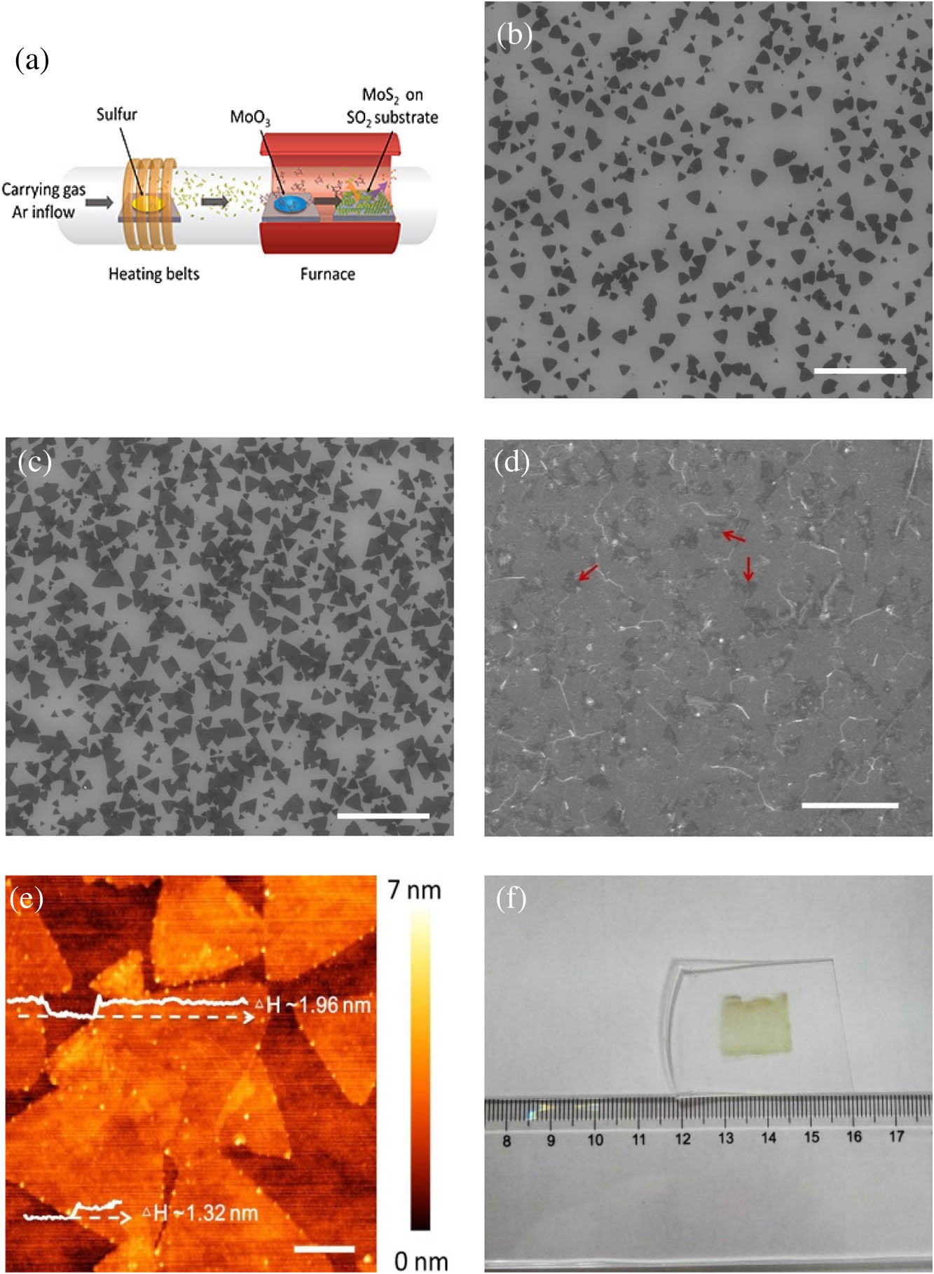
    Fig. 1. Material characterizations of MoS2; (a) schematic diagram showing the chemical synthesis of MoS2; (b–d) SEM images showing different growth stages of MoS2 with different reaction times of 5, 12, and 30 min, respectively. Scale bars, 10 μm; (e) AFM topography of MoS2 film on SiO2 substrate. Bottom and top white profiles indicate bilayer and trilayers, respectively. Scale bar, 1 μm; (f) optical image of large-area MoS2 film transferred onto PDMS substrate.
    Spectroscopic characterizations of MoS2 films; (a) Raman spectra of few-layer MoS2 on SiO2/Si substrate; (b) PL spectrum of few-layer MoS2 film; (c) UV−visible spectrum of few-layer MoS2 film on quartz.
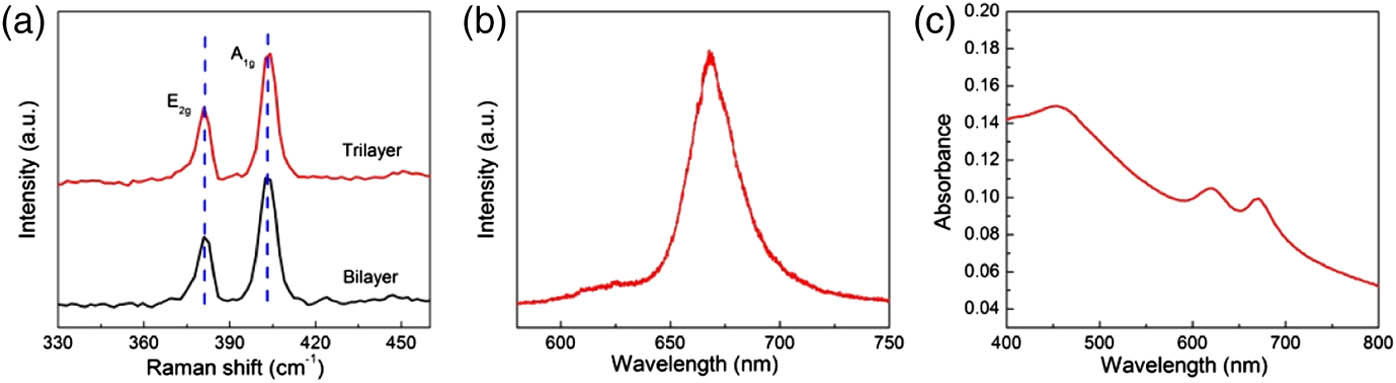
    Fig. 2. Spectroscopic characterizations of MoS2 films; (a) Raman spectra of few-layer MoS2 on SiO2/Si substrate; (b) PL spectrum of few-layer MoS2 film; (c) UV−visible spectrum of few-layer MoS2 film on quartz.
    (a) TEM image showing folded MoS2 film. Scale bar, 100 nm; (b) HRTEM image of MoS2 film. Scale bar, 5 nm. Inset, corresponding electron diffraction pattern; (c) XPS spectrum of MoS2 thin film; (d) XRD result for MoS2 thin film.
    Fig. 3. (a) TEM image showing folded MoS2 film. Scale bar, 100 nm; (b) HRTEM image of MoS2 film. Scale bar, 5 nm. Inset, corresponding electron diffraction pattern; (c) XPS spectrum of MoS2 thin film; (d) XRD result for MoS2 thin film.
    (a) Typical transfer curve for MoS2 transistor. Inset, optical image of a FET device. Scale bar, 100 μm; (b) output curve for MoS2 transistor.
    Fig. 4. (a) Typical transfer curve for MoS2 transistor. Inset, optical image of a FET device. Scale bar, 100 μm; (b) output curve for MoS2 transistor.
    Caiyun Chen, Hong Qiao, Yunzhou Xue, Wenzhi Yu, Jingchao Song, Yao Lu, Shaojuan Li, Qiaoliang Bao. Growth of large-area atomically thin MoS2 film via ambient pressure chemical vapor deposition[J]. Photonics Research, 2015, 3(4): 110
    Download Citation