Abstract
Atomically thin MoS2 films have attracted significant attention due to excellent electrical and optical properties. The development of device applications demands the production of large-area thin film which is still an obstacle. In this work we developed a facile method to directly grow large-area MoS2 thin film on SiO2 substrate via ambient pressure chemical vapor deposition method. The characterizations by spectroscopy and electron microscopy reveal that the as-grown MoS2 film is mainly bilayer and trilayer with high quality. Back-gate field-effect transistor based on such MoS2 thin film shows carrier mobility up to 3.4 cm2 V?1 s?1 and on/off ratio of 105. The large-area atomically thin MoS2 prepared in this work has the potential for wide optoelectronic and photonic device applications.1. INTRODUCTION
Atomic-layered molybdenum disulfide (), a new two-dimensional (2D) material, has gained intense attention due to its outstanding electrical and optical properties [1–5]. When bulk is reduced to monolayer sheet, an indirect-to-direct bandgap transition occurs, leading to extremely high quantum efficiency for light emission [6,7]. Compared with graphene, has a visible bandgap to allow the field-effect transistors based on this material to be effectively switching off. Moreover, the carrier mobility is impressively high, up to in theory [8] and demonstrated in experiments [2] for monolayer . In order to fulfill the demands for device applications, substantial efforts have been devoted into synthesize atomically thin film, including micromechanical exfoliation [4,5,9,10], liquid exfoliation [11–13], and physical vapor deposition [14]. However, films are often limited to their micrometer size, which hinders large-scale device applications. Hence, it is critical to develop practical methods to grow large-area thin film aiming for device fabrications.
Similar to the growth of large-area graphene film, chemical vapor deposition (CVD) has been successfully applied to synthesize large-area film. Zhan et al. [15] reported the production of large-area few-layer film through sulfiding the substrate but the thin films possess poor quality. Alternatively, the thermal decomposition of [16] in the presence of mixed gas could also induce large-area thin film; however, the pre-deposition of precursors by dip-coating lacks the control of thickness. Lee et al. [17] chose powder as precursor for CVD growth of thin films by seeding the substrate with reduced graphene oxides. The resulting product may have contamination of the seeds. Recently, Yu et al. [18] reported a self-limiting CVD approach to produce large-area thin films on various substrates but a very low carrier mobility () was achieved.
In this work, we report a seedless and scalable growth method using ambient pressure CVD to produce high quality few-layer thin film. Compared with previous reports which used low-pressure CVD to grow [18,19], the present method has simpler operation procedures and better repeatabilities. The as-grown on is suitable for following device fabrication without transfer process which could induce defects and impurities. The scalable growth method can be further adopted to more complicated photonic structures such as waveguides and gratings, affording compatability with integrated photonic circuits.
Sign up for Photonics Research TOC. Get the latest issue of Photonics Research delivered right to you!Sign up now
2. RESULTS AND DISCUSSION
Figure 1(a) schematically shows the experimental setup to synthesize thin film on substrate. The sulfur powder was located at upstream of the CVD system. The powder was placed in a quartz boat in the furnace and the substrate was next to the source. During the growth, sulfur and were heated to 100°C and 650°C, respectively. The carrying gas argon was at a flow rate of 150 sccm and the system was kept at ambient pressure. As illustrated in Fig. 1(a), is reduced by sulfur vapor to form species [17,20], which will diffuse to substrate and eventually lead to nucleation and growth of thin film.
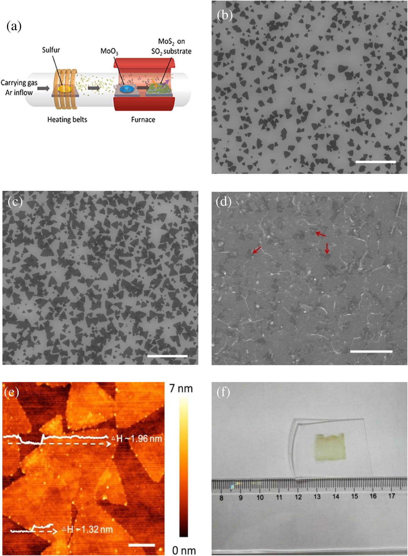
Figure 1.Material characterizations of ; (a) schematic diagram showing the chemical synthesis of ; (b–d) SEM images showing different growth stages of with different reaction times of 5, 12, and 30 min, respectively. Scale bars, 10 μm; (e) AFM topography of film on substrate. Bottom and top white profiles indicate bilayer and trilayers, respectively. Scale bar, 1 μm; (f) optical image of large-area film transferred onto PDMS substrate.
Figures 1(b)–1(d) show scanning electron microscope (SEM) images of films with different morphologies. The growth times are 5, 12, and 30 min for Figs. 1(b), 1(c), and 1(d), respectively, with the same growth temperature of 650°C. It is found that these samples represent different growth stages. At the early stage of growth, the triangle-shaped crystals randomly distribute on substrate, as shown in Fig. 1(b). Upon prolonging the growth time to 12 min, smaller grains turn into larger ones by adsorbing atoms, as indicated in Fig. 1(c). It should be noted that the crystals tend to interconnect rather than overlap with each other when they grow larger. When the growth time is prolonged to 30 min, full coverage of film was achieved due to the coalescence of large crystals, as shown in Fig. 1(d). The uniformity is verified by the small difference in the contrast over the whole film. The white color lines mainly correspond to gaps among crystals. When film is fully covered on the substrate, incoming species will nucleate to form thicker triangle crystals (as indicated by the red arrows), whereas a small portion of them will aggregate to form curved nanoparticles or quasi-one-dimensional nanowires.
Figure 1(e) shows the representative atomic force microscopy (AFM) topography of film on substrate. It reveals a few triangular domains interconnecting with each other. The homogeneous color contrast indicates good uniformity. The line profiles indicate thickness of about 1.32 and 1.96 nm, corresponding to bilayer [18] and trilayer film [21]. The few-layer thin film grown on substrate can be completely peeled off and transferred to other arbitrary substrates. Figure 1(f) shows a centimeter-size film which was transferred onto polydimethylsiloxane (PDMS) film with good continuity.
Spectroscopic characterizations were carried out to evaluate the quality of film. Figure 2(a) shows Raman spectra of the as-grown film measured at the excitation of 514 nm, which reveals two characteristic peaks. The peak is around attributed to the in-plane mode resulting from opposite vibration of two S atoms with respect to the Mo atom. The peak is around assigned to the mode which is associated with the out-of-plane vibration of only S atoms in the opposite directions [22,23]. The frequency difference () between and increases with the thickness, which can be used to identify the number of layer in atomic layered [16,20,24]. In this context Δ is calculated to be and , corresponding to bilayer and trilayer film, respectively [21,22]. Figure 2(b) shows the photoluminescence (PL) spectrum (with 514 nm laser excitation) which also consists of two pronounced emission peaks at around 625 and 670 nm. The strong light emission corresponds to the direct excitonic transitions at the Brillouin zone K point [20]. The appearance of these two emission peaks is in consistent with two excitonic absorption bands around 620 and 670 nm shown in the UV−visible spectrum [Fig. 2(c)].

Figure 2.Spectroscopic characterizations of films; (a) Raman spectra of few-layer on substrate; (b) PL spectrum of few-layer film; (c) UV−visible spectrum of few-layer film on quartz.
Transmission electron microscopy (TEM) is also employed to characterize the quality and crystal structure of transferred film. Figure 3(a) shows the microstructure of a piece of film folded on TEM grid. The high-resolution TEM (HRTEM) image clearly resolves the lattice of few-layer film. The selected area electron diffraction (SAED) pattern in the inset of Fig. 3(b) contains multi-group 6-fold symmetry spots, which indicates that the measured zone of film contains several grains possessing different crystal orientations. Meanwhile, the X-ray photoelectron spectroscopy (XPS) results shown in Fig. 3(c) reveal the binding energies of and at 232.5 and 229.3 eV, respectively. Two peaks located at 163.2 and 162.0 eV are attributed to and , respectively. These binding energy results are in good consistent with previous reports [25,26], suggesting the successful growth of layered film. The X-ray diffraction (XRD) profile for few-layer is shown in Fig. 3(d). The diffraction peaks at 14.4° and 33.1° are attributed to the (002) and (100) crystal planes, respectively [6,16].
Figure 3.(a) TEM image showing folded film. Scale bar, 100 nm; (b) HRTEM image of film. Scale bar, 5 nm. Inset, corresponding electron diffraction pattern; (c) XPS spectrum of thin film; (d) XRD result for thin film.
To investigate the electrical performance of our sample, we fabricated back gate field-effect transistors using few-layer directly grown on substrate. The typical transfer versus curve of transistor device is shown in Fig. 4(a). We can extract the device on-off ratio up to , which is sufficiently high for transistor device based on few-layer considering that back gate structure was used. Furthermore, the calculated field effect carrier mobility turns out to be via , where is the dielectric constant of ; and are the channel length and channel width, respectively. It is worth noting that the room temperature carrier mobility of our device is comparable to that based on monolayer with the similar configuration, which are usually in the range of [27,28]. Figure 4(b) shows output characteristics of the few-layer device. It is seen that the drain current is dependent on the drain–source voltage at various back-gate voltages, which implies good gate tunability of our device.
Figure 4.(a) Typical transfer curve for transistor. Inset, optical image of a FET device. Scale bar, 100 μm; (b) output curve for transistor.
3. CONCLUSION
In summary, we have successfully developed a facile method to grow large-area on substrate via ambient pressure CVD. The material characterization results show that our films are mainly two to three atomic layers with good uniformity and high quality. The few-layer thin film show good electrical properties, i.e., the mobility of our transistor is comparable to that of transistors based on monolayer flakes. Our work provides a route toward scalable growth of high-quality few-layer film and the thin films are ideal materials for electronics and optoelectronic devices.
4. EXPERIMENTAL SECTION
A. Materials Synthesis
The films were synthesized on substrates ( thickness, 300 nm) via CVD technique. The substrates were cleaned in acetone and isopropanol successively. Prior to the growth, argon gas (99.999%) was used to clean the growth chamber at room temperature. High-purity (99.5%, Alfa Aesar) and sulfur powder (99.5%, Sinopharm Chemical Reagent, Shanghai Co., Ltd.) were kept in two separate quartz boats in the furnace with the substrates placed downstream of the CVD system. For the growth of , the furnace was heated up to 650°C and maintained for 30 min, while the argon gas was purging with a flow rate of 150 sccm at ambient pressure. Afterward, the furnace was cooled down naturally to room temperature.
B. Material Characterization
Raman and PL spectra were collected by micro-Raman system (Horiba Jobin Yvon, HR800). The excitation wavelength is 514 nm, and the laser spot is focused to with objective lens. UV-visible absorption spectra were obtained by UV-visible-IR spectrometer (PerkinElmer, Lambda750 system). Chemical composition and crystal orientation were studied using XPS (KRATOS Analytical, KRATOS AXIS Ultra DLD) and XRD (PANPANalytical B.V.P, Ruki). Surface morphology of the samples was examined by SEM (FEI, Quanta 200 FEG) and AFM (Bruker, Dimension Icon). TEM (FEI, Tecnai G2 F20) was used to investigate the microstructures.
C. Fabrication of Transistors
The transistor devices were directly fabricated on films grown on substrates. The highly doped -type silicon of substrate serves as the back-gate electrode. The device fabrication includes UV lithography to define the device pattern and electron-beam evaporation to deposit source and drain electrodes (100 nm Au on top of 5 nm Ti).
D. Electrical Measurements
The measurements were performed by probe station (Cascade M150) equipped with a semiconductor property analyzer (Keithley 2400) at room temperature in ambient conditions.
References
[1] D. Lembke, A. Kis. Breakdown of high-performance monolayer MoS2 transistors. ACS Nano, 6, 10070-10075(2012).
[2] H. Schmidt, S. Wang, L. Chu, M. Toh, R. Kumar, W. Zhao, A. H. Castro Neto, J. Martin, S. Adam, B. Özyilmaz. Transport properties of monolayer MoS2 grown by chemical vapor deposition. Nano Lett., 14, 1909-1913(2014).
[3] B. W. Baugher, H. O. Churchill, Y. Yang, P. Jarillo-Herrero. Intrinsic electronic transport properties of high-quality monolayer and bilayer MoS2. Nano Lett., 13, 4212-4216(2013).
[4] A. Splendiani, L. Sun, Y. Zhang, T. Li, J. Kim, C.-Y. Chim, G. Galli, F. Wang. Emerging photoluminescence in monolayer MoS2. Nano Lett., 10, 1271-1275(2010).
[5] B. Radisavljevic, A. Radenovic, J. Brivio, V. Giacometti, A. Kis. Single-layer MoS2 transistors. Nat. Nanotechnol., 6, 147-150(2011).
[6] S. Balendhran, J. Z. Ou, M. Bhaskaran, S. Sriram, S. Ippolito, Z. Vasic, E. Kats, S. Bhargava, S. Zhuiykov, K. Kalantar-Zadeh. Atomically thin layers of MoS2 via a two step thermal evaporation-exfoliation method. Nanoscale, 4, 461-466(2012).
[7] M. Chhowalla, H. S. Shin, G. Eda, L. J. Li, K. P. Loh, H. Zhang. The chemistry of two-dimensional layered transition metal dichalcogenide nanosheets. Nat. Chem., 5, 263-275(2013).
[8] K. Kaasbjerg, K. S. Thygesen, K. W. Jacobsen. Phonon-limited mobility in n-type single-layer MoS2 from first principles. Phys. Rev. B, 85, 115317(2012).
[9] S. Ghatak, A. N. Pal, A. Ghosh. Nature of electronic states in atomically thin MoS2 field-effect transistors. ACS Nano, 5, 7707-7712(2011).
[10] H. Liu, A. T. Neal, P. D. Ye. Channel length scaling of MoS2 MOSFETs. ACS Nano, 6, 8563-8569(2012).
[11] H. Hwang, H. Kim, J. Cho. MoS2 nanoplates consisting of disordered graphene-like layers for high rate lithium battery anode materials. Nano Lett., 11, 4826-4830(2011).
[12] Y. Yao, Z. Lin, Z. Li, X. Song, K.-S. Moon, C.-P. Wong. Large-scale production of two-dimensional nanosheets. J. Mater. Chem., 22, 13494-13499(2012).
[13] J. N. Coleman, M. Lotya, A. O’Neill, S. D. Bergin, P. J. King, U. Khan, K. Young, A. Gaucher, S. De, R. J. Smith. Two-dimensional nanosheets produced by liquid exfoliation of layered materials. Science, 331, 568-571(2011).
[14] S. Wu, C. Huang, G. Aivazian, J. S. Ross, D. H. Cobden, X. Xu. Vapor-solid growth of high optical quality MoS2 monolayers with near-unity valley polarization. ACS Nano, 7, 2768-2772(2013).
[15] Y. Zhan, Z. Liu, S. Najmaei, P. M. Ajayan, J. Lou. Large-area vapor-phase growth and characterization of MoS2 atomic layers on a SiO2 substrate. Small, 8, 966-971(2012).
[16] K. K. Liu, W. Zhang, Y. H. Lee, Y. C. Lin, M. T. Chang, C. Y. Su, C. S. Chang, H. Li, Y. Shi, H. Zhang. Growth of large-area and highly crystalline MoS2 thin layers on insulating substrates. Nano Lett., 12, 1538-1544(2012).
[17] Y. H. Lee, X. Q. Zhang, W. Zhang, M. T. Chang, C. T. Lin, K. D. Chang, Y. C. Yu, J. T. W. Wang, C. S. Chang, L. J. Li. Synthesis of large-area MoS2 atomic layers with chemical vapor deposition. Adv. Mater., 24, 2320-2325(2012).
[18] Y. Yu, C. Li, Y. Liu, L. Su, Y. Zhang, L. Cao. Controlled scalable synthesis of uniform, high-quality monolayer and few-layer MoS2 films. Sci. Rep., 3, 1866(2013).
[19] J. Zhang, H. Yu, W. Chen, X. Tian, D. Liu, M. Cheng, G. Xie, W. Yang, R. Yang, X. Bai. Scalable growth of high-quality polycrystalline MoS2-monolayers on SiO2 with tunable grain sizes. ACS Nano, 8, 6024-6030(2014).
[20] Q. Ji, Y. Zhang, T. Gao, Y. Zhang, D. Ma, M. Liu, Y. Chen, X. Qiao, P.-H. Tan, M. Kan. Epitaxial monolayer MoS2 on mica with novel photoluminescence. Nano Lett., 13, 3870-3877(2013).
[21] D.-S. Tsai, K. K. Liu, D. H. Lien, M. L. Tsai, C. F. Kang, C. A. Lin, L. J. Li, J. H. He. Few-layer MoS2 with high broadband photogain and fast optical switching for use in harsh environments. ACS Nano, 7, 3905-3911(2013).
[22] H. Li, Q. Zhang, C. C. R. Yap, B. K. Tay, T. H. T. Edwin, A. Olivier, D. Baillargeat. From bulk to monolayer MoS2: Evolution of Raman scattering. Adv. Funct. Mater., 22, 1385-1390(2012).
[23] X. Zhang, W. Han, J. Wu, S. Milana, Y. Lu, Q. Li, A. Ferrari, P. Tan. Raman spectroscopy of shear and layer breathing modes in multilayer MoS2. Phys. Rev. B, 87, 115413(2013).
[24] H. Li, Z. Yin, Q. He, H. Li, X. Huang, G. Lu, D. W. H. Fam, A. I. Y. Tok, Q. Zhang, H. Zhang. Fabrication of single-and multilayer MoS2 film-based field-effect transistors for sensing no at room temperature. Small, 8, 63-67(2012).
[25] X. Wang, H. Feng, Y. Wu, L. Jiao. Controlled synthesis of highly crystalline MoS2 flakes by chemical vapor deposition. J. Am. Chem. Soc., 135, 5304-5307(2013).
[26] C. Altavilla, M. Sarno, P. Ciambelli. A novel wet chemistry approach for the synthesis of hybrid 2D free-floating single or multilayer nanosheets of MS2 @ oleylamine (M, Mo, W). Chem. Mater., 23, 3879-3885(2011).
[27] K. Novoselov, D. Jiang, F. Schedin, T. Booth, V. Khotkevich, S. Morozov, A. Geim. Two-dimensional atomic crystals. Proc. Natl. Acad. Sci. USA, 102, 10451-10453(2005).
[28] J. Lin, J. Zhong, S. Zhong, H. Li, H. Zhang, W. Chen. Modulating electronic transport properties of MoS2 field effect transistor by surface overlayers. Appl. Phys. Lett., 103, 063109(2013).


