• Photonics Research
  • Vol. 10, Issue 1, 41 (2022)
Caifu Fan1, Xi Shi2、4、*, Feng Wu3, Yunhui Li1, Haitao Jiang1, Yong Sun1、5、*, and Hong Chen1
Author Affiliations
  • 1MOE Key Laboratory of Advanced Micro-Structured Materials, School of Physics Science and Engineering, Tongji University, Shanghai 200092, China
  • 2Department of Physics, Shanghai Normal University, Shanghai 200234, China
  • 3School of Optoelectronic Engineering, Guangdong Polytechnic Normal University, Guangzhou 510665, China
  • 4e-mail: xishi@shnu.edu.cn
  • 5e-mail: yongsun@tongji.edu.cn
  • show less
    DOI: 10.1364/PRJ.441278 Cite this Article Set citation alerts
    Caifu Fan, Xi Shi, Feng Wu, Yunhui Li, Haitao Jiang, Yong Sun, Hong Chen. Photonic topological transition in dimerized chains with the joint modulation of near-field and far-field couplings[J]. Photonics Research, 2022, 10(1): 41 Copy Citation Text show less
    (a) 1D dimerized chain with the unit cell length L and the distance d between two sites An and Bn. Δ=d/L is the dimerized parameter. Two sites An and Bn are both coupled to the backbone waveguide at the same coupling rate γ, and they are directly coupled to each other through near field at a coupling rate κ. (b) Schematic of the unit cell excited by the left and right incident EM waves noted as SL+ and SR+. The output EM waves from two sides are noted as SL− and SR−. (c) Reflectivity and (d) reflection phase for a semi-infinite 1D chain modulated by the dimerized parameter Δ with the vanished near-field coupling (κ=0). The first and second band gaps are noted as G1 and G2 in (c). The second and third pass bands are inversed for the 1D dimerized chain with two different dimerized parameters Δ=0.165 and Δ=0.25 (denoted by the white dashed lines). The reflection phases of these two cases for the second band gap have different signs.
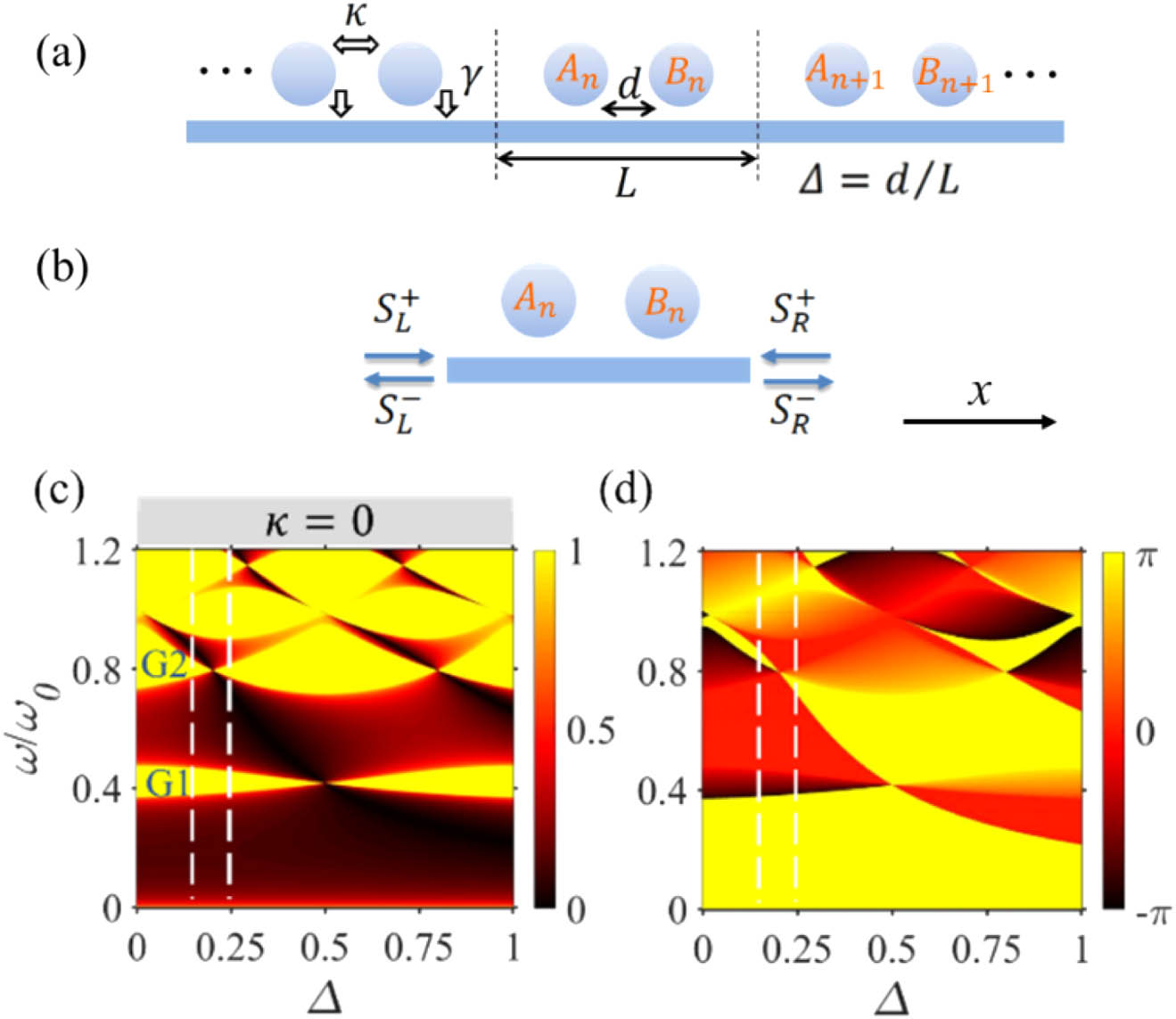
    Fig. 1. (a) 1D dimerized chain with the unit cell length L and the distance d between two sites An and Bn. Δ=d/L is the dimerized parameter. Two sites An and Bn are both coupled to the backbone waveguide at the same coupling rate γ, and they are directly coupled to each other through near field at a coupling rate κ. (b) Schematic of the unit cell excited by the left and right incident EM waves noted as SL+ and SR+. The output EM waves from two sides are noted as SL and SR. (c) Reflectivity and (d) reflection phase for a semi-infinite 1D chain modulated by the dimerized parameter Δ with the vanished near-field coupling (κ=0). The first and second band gaps are noted as G1 and G2 in (c). The second and third pass bands are inversed for the 1D dimerized chain with two different dimerized parameters Δ=0.165 and Δ=0.25 (denoted by the white dashed lines). The reflection phases of these two cases for the second band gap have different signs.
    (a) Reflectivity and (b) reflection phase of the semi-infinite 1D dimerized chain with intracell near-field coupling κ=−0.044ω0. Similarly, (c) and (d) are the reflectivity and reflection phase of the 1D chain with the near-field coupling κ=−0.137ω0. For a fixed dimerized parameter Δ=0.165 indicated by the white dashed lines in (a)–(d), the second band gap closes in (a) and reopens in (c).
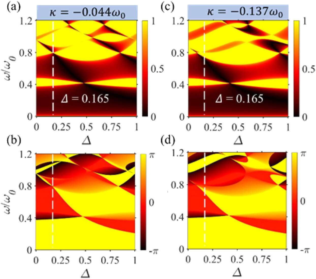
    Fig. 2. (a) Reflectivity and (b) reflection phase of the semi-infinite 1D dimerized chain with intracell near-field coupling κ=0.044ω0. Similarly, (c) and (d) are the reflectivity and reflection phase of the 1D chain with the near-field coupling κ=0.137ω0. For a fixed dimerized parameter Δ=0.165 indicated by the white dashed lines in (a)–(d), the second band gap closes in (a) and reopens in (c).
    (a) Reflectivity and (b) reflection phase of the semi-infinite 1D dimerized chain as functions of near-field coupling and frequency for a specific dimerized parameter Δ=0.165. The gradually increased near-field coupling strength leads to the band inversion for the second and third bands. The second band gap closes at κ=−0.047ω0.
    Fig. 3. (a) Reflectivity and (b) reflection phase of the semi-infinite 1D dimerized chain as functions of near-field coupling and frequency for a specific dimerized parameter Δ=0.165. The gradually increased near-field coupling strength leads to the band inversion for the second and third bands. The second band gap closes at κ=0.047ω0.
    Band structures of infinite 1D dimerized chain for a fixed dimerized parameter Δ=0.165, but different near-field coupling strengths. The gray shadows in (a) indicate band gaps marked as G1–G4, and the pass bands represented by the black lines are noted as B1–B4. The Zak phases for each band are marked. For other cases from (b) to (f), only the Zak phases are noted in the diagrams. The effective permittivity εeff and permeability μeff for the band gaps are plotted. The materials with εeff<0 are the epsilon-negative materials (ENG) while the materials with μeff<0 are mu-negative materials (MNG). ENG and MNG own different topological properties.
    Fig. 4. Band structures of infinite 1D dimerized chain for a fixed dimerized parameter Δ=0.165, but different near-field coupling strengths. The gray shadows in (a) indicate band gaps marked as G1–G4, and the pass bands represented by the black lines are noted as B1–B4. The Zak phases for each band are marked. For other cases from (b) to (f), only the Zak phases are noted in the diagrams. The effective permittivity εeff and permeability μeff for the band gaps are plotted. The materials with εeff<0 are the epsilon-negative materials (ENG) while the materials with μeff<0 are mu-negative materials (MNG). ENG and MNG own different topological properties.
    Zak phase diagram of the second band under the joint modulation of near-field coupling κ and the far-field coupling (dimerized parameter Δ). The first band gap is closed for the κ and Δ indicated by the black dashed line while the second band gap is closed for the κ and Δ represented by the two white dashed lines.
    Fig. 5. Zak phase diagram of the second band under the joint modulation of near-field coupling κ and the far-field coupling (dimerized parameter Δ). The first band gap is closed for the κ and Δ indicated by the black dashed line while the second band gap is closed for the κ and Δ represented by the two white dashed lines.
    (a) Three samples of 1D chain for (I) dimerized parameter Δ=0.165, near-field coupling κ=0, (II) dimerized parameter Δ=0.165, near-field coupling κ=−0.12ω0, and (III) pairing of two aforementioned samples to demonstrate the topological interface state. The samples are fabricated on the Rogers RT 5880 double-side copper-clad board. The reflectivity and reflection phases for sample I and sample II are experimentally and theoretically shown in (b) and (c), respectively. The gray shadows indicate the band gaps. The reflection for the sample III is shown in (d), where the shadows are band gaps. There is a small valley only in the second band gap, which indicates the existence of an interface state. The electric field amplitude distribution of the interface state is measured and compared to the simulation results in (e).
    Fig. 6. (a) Three samples of 1D chain for (I) dimerized parameter Δ=0.165, near-field coupling κ=0, (II) dimerized parameter Δ=0.165, near-field coupling κ=0.12ω0, and (III) pairing of two aforementioned samples to demonstrate the topological interface state. The samples are fabricated on the Rogers RT 5880 double-side copper-clad board. The reflectivity and reflection phases for sample I and sample II are experimentally and theoretically shown in (b) and (c), respectively. The gray shadows indicate the band gaps. The reflection for the sample III is shown in (d), where the shadows are band gaps. There is a small valley only in the second band gap, which indicates the existence of an interface state. The electric field amplitude distribution of the interface state is measured and compared to the simulation results in (e).
    (a) Schematic of a side resonant branch excited by the EM waves from Port1 and (b) the simulation (black line) and fitted reflectivity (red line) of the EM wave. (c) Near-field coupling and far-field coupling coexist between two resonant branches in the same unit cell and (d) the simulation (black line) and fitted reflectivity (red line) when the EM wave is incident from the left.
    Fig. 7. (a) Schematic of a side resonant branch excited by the EM waves from Port1 and (b) the simulation (black line) and fitted reflectivity (red line) of the EM wave. (c) Near-field coupling and far-field coupling coexist between two resonant branches in the same unit cell and (d) the simulation (black line) and fitted reflectivity (red line) when the EM wave is incident from the left.
    Caifu Fan, Xi Shi, Feng Wu, Yunhui Li, Haitao Jiang, Yong Sun, Hong Chen. Photonic topological transition in dimerized chains with the joint modulation of near-field and far-field couplings[J]. Photonics Research, 2022, 10(1): 41
    Download Citation