• Journal of Semiconductors
  • Vol. 41, Issue 1, 010301 (2020)
Ning Zhuo, Fengqi Liu, and Zhanguo Wang
Author Affiliations
  • Key Laboratory of Semiconductor Materials Science, Institute of Semiconductors, Chinese Academy of Sciences, Beijing 100083, China
  • show less
    DOI: 10.1088/1674-4926/41/1/010301 Cite this Article
    Ning Zhuo, Fengqi Liu, Zhanguo Wang. Quantum cascade lasers: from sketch to mainstream in the mid and far infrared[J]. Journal of Semiconductors, 2020, 41(1): 010301 Copy Citation Text show less

    Abstract

    Electrically-pumped semiconductor lasers based on monolithic chip configuration possess plenty of advantages such as small volume, light weight, long lifetime and stable performance. Nevertheless this type of lasers rely on the interband transition, which sets the bounds for emission wavelength typically below 4 μm, and state of the art performance has been attained below 3 μm. Attempts to employ small bandgap meterials like antimonide or lead salts ended with poor performance mainly due to imperfect crystal quality and severe Auger recombination. In view of the broad application prospects of infrared spectral range above 3 μm, more attention was casted again on the low-dimensional quantum structure materials, such as quantum wells and quantum dots, which have been applied in the near infrared successfully decades ago. One of the most basic characteristics of low-dimensional quantum structure is the quantization of sub levels (subbands) in conduction or valence band, in other words, the levels where carrier can populate are discretized from the continuous states of the bulk bands of bulk materials, namely the quantum size effect. When the size of the quantum wells or quantum dots varies from several angstroms to tens of nanometers, the spacing of these discrete energy levels can cover the range from 3 to 300 μmin principle. However, to guide carriers to make such fine subband transitions at the nm and meV scales and thus achieve optical amplification of emission, is such a quite bold idea that it was widely considered impossible once the initial concept of subband transition for light amplification was proposed. The intrasubband and intersubband dynamic process of carriers is so fast (orders of picosecond) that it is quite tough to realize population inversion between subbands under conventional electric injection level, meaning extremely high threshold current density is required. In order to realize carrier accumulation on specific subband, using single quantum well and barrier as functional primitives, a series of quantum wells are connected in a cascade to form an artificial ordered structure. After delicate design of quantum scattering between subbands to achieve locally different scattering rate distribution, a most complicated ever low-dimensional heterogeneous structure model with up to thousands of ultra thin layers was established. With a combination of advanced monolayer epitaxial technologies, this novel intersubband laser achieved impressive and remarkable device performance in the mid and far infrared and commercially available among most of spectral range at present.

    1. What is quantum cascade laser?

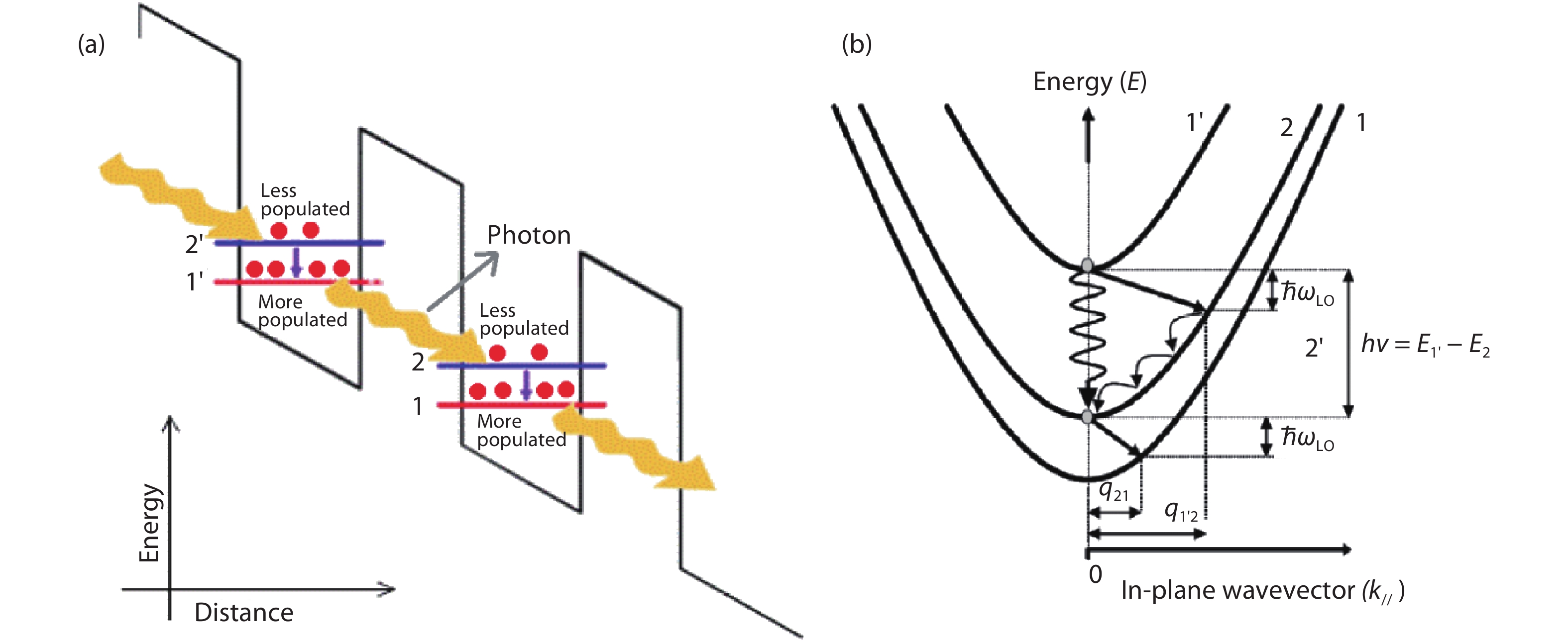
    Quantum cascade lasers (QCLs) are a rising type of semiconductor lasers and characterized by unique operating principle in comparison with its predecessors, i.e. diode lasers. The most outstanding characteristic of QCLs should be the extraordinary ability of wavelength coverage, theoretically from 3 far to 300 μm, even without the necessity of changing elementary gain materials. Similar to the conventional diode lasers, QCLs basically comprise substrate, low-refractive index lower & upper waveguide cladding layers, and gain region which is multi-layered and quite thicker. We call QCLs the intraband lasers in marked contrast to interband laser which diode lasers belong to. The “intraband” means that carriers driven by external electric field flow directionally in one type of energy band, in practice electrons in conduction band without the interplay of lower valance band. The key strategy to accomplish this task is the utilization of n-doped quantum well and quantum tunneling, which breaks continuous conduction band into a series of semi-discrete subbands in K space and form a string of energy levels spacing from several meV to hundreds of meV due to quantum size confinement effect in quantum well. So the functional elements of QCLs are quantum wells and barriers. Due to the nanoscale barriers, quantum wells are strongly intercoupled resulting in delocalized subband wavefunctions, which is beneficial for efficient electron transition between overlapped states. After applying a certain external electric field the situation of subbands distribution changes a bit, i.e. a series of energy steps or named ladder formed due to added inclined electric potential field. Following the direction of electric field electrons jumps downstream from one subband to another, accompanied by emission or absorption of photons or phonons. The underlying operating mechanism of QCLs is basically a four-level system illustrated in Fig. 1(a), reminiscent of gas or dye lasers, where electrons are injected from level 2’ to level 1’ by resonant tunneling or phonon-assisted scattering, followed by phonon or photon-assisted scattering process from level 1’ to level 2 (in the downstream quantum well) which contributes to spontaneous and stimulated emission of photons of certain frequency, and ended with fast depletion of electrons from level 2 to level 1 in the downstream quantum well (refer to Fig. 1(b)). In fact the prototype in 1970s[1] consists of only two pairs of quantum well & barriers, and four levels in two quantum wells complete the trilogy, namely injection, photon emission and depletion. One byproduct of intraband transition in inclined electric potential profile is the feasibility of recycling electrons after depleted from previous stage, which means electrons are re-injected into the following stage and then repeat the same “old story”, as many times as one wishes. This “cascade” feature is essential for improving confinement factor of infrared waveguide mode, and meanwhile lowering parasitic series resistance power consumption owing to lower injection current demand of vertically stacked gain region compared with high current injection of broad-area single gain stage configuration. Other typical traits of QCLs include high-speed electrical response due to subband scattering lifetime of picosecond order of magnitude, and narrow gain spectrum rooted in curvature of dispersive curve of all related subbands with same signs.

    (Color online) (a) Basic four-level system for intersubband lasers and (b) fast LO-phonon scattering process between and in subbands.

    Figure 1.(Color online) (a) Basic four-level system for intersubband lasers and (b) fast LO-phonon scattering process between and in subbands.

    2. Milestones and state of the art performance

    Since the advent of first prototype of QCLs in 1994[2], steady improvements have been made toward such as room temperature continuous wave operation, high output power, broad spectrum coverage and low power consumption, mainly owing to modern crystal growth techniques with unprecedented control accuracy of single atomic monolayer such as molecular beam epitaxy (MBE) and metallorganic chemical vapor deposition (MOCVD), and on the other hand thorough understanding of underlying operating mechanism and continuous refinement of gain region design. At present typical active core, i.e. gain region of mid infrared QCLs, as illustrated in Fig. 2(a), comprises 30 to 50 identical cascade stages and each stage contains about ten pairs of ultra thin well & barriers, resulting in thousands of nanolayers in the whole active core. Functionally each stage could be divided further into photon-related active region and phonon-related injection/extraction region ( Fig. 2(b)), which in deed is the soul of QCLs that makes intersubband lasers into reality finally. Electrons in injection/extraction region move faster than in active region qualitatively, which results in local population accumulation, i.e. population inversion in the latter. Thanks to the well-known ultrafast intersubband LO-phonon assisted scattering process this special and elaborate regulation of carriers quantum transport dynamics could be engineered naturally by means of shrinking spacing of energy levels in extraction region close to LO-phonon energy while maintaining interval of lasing levels for photon emission of designed frequency. Electrons in upper lasing level in active region have a typical LO-phonon scattering lifetime of about 1 ps, while ones in lower lasing level experience a faster depletion time of the order of 0.1 ps. Bearing in mind that typical carrier lifetime in interband lasers has an order of nanosecond, it would be very tough for QCLs to reach threshold current due to ultrafast carrier consumption (nonradiative scattering) rate. However, population inversion (prerequisite for laser) could be attained with the minimum requirement that the ratio of upper lasing level lifetime and lower one is greater than 1 regardless of orders of lifetime. After positive population inversion guaranteed, the left work became very clear: enhancing injection efficiency, prolonging upper lasing level lifetime and shortening lower level one further, aiming at lower threshold current density and higher internal quantum efficiency necessary for room temperature (RT) continuous wave (CW) operation devices. A series of simulation methods have been developed successively to forecast the dynamic behavior of a specific design, such as rate equation model, density matrix method, non-equilibrium Green’s function simulation and Monte Carlo analysis.

    (Color online) (a) Typical mid infrared QCL structure and (b) subband diagram of gain region under applied electric field.

    Figure 2.(Color online) (a) Typical mid infrared QCL structure and (b) subband diagram of gain region under applied electric field.

    First QCL was based on strain-compensated InGaAs/InAlAs multi coupled quantum wells grow by MBE and gain region design of diagonal transition plus single phonon resonance extraction (Fig. 3(a)). This device worked up to 90 K at 4.2 μm with peak power in excess of 8 mW. The following was another lattice-matched 8 μm QCL[3] utilizing superlattice as active region which worked up to 200 K with 800 mW power at 80 K in 1997 (Fig. 3(b)). This superlatttice device benefited a lot from intrinsic contrast of carrier relaxation lifetimes between intramimiband and interminiband scattering and larger dipole matrix element, thanks to the stronger coupled quantum wells closely spaced in superlattice. Another breakthrough based on superlattice active region came in 2001, that first far infrared QCL[4] operating at 68 μm, down to terahertz region, was demonstrated with peak output power of more than 2 mW at 8 K.

    (Color online) Representative evolution roadmaps for (a) multi quantum wells design (Refs. [2, 5, 8]) and (b) superlattice design (Refs. [3, 6, 11]).

    Figure 3.(Color online) Representative evolution roadmaps for (a) multi quantum wells design (Refs. [2, 5, 8]) and (b) superlattice design (Refs. [3, 6, 11]).

    Aiming at RT CW operation the following refining strategies relating to laser active region includes two main directions, which both concentrate on high-efficiency carrier transport trilogy, i.e. high-efficiency injection, photon emission and depletion. One is to add one or more LO-phonon energy spaced quantum wells after single phonon resonance extraction level for multi coupled quantum wells design, forming so-called double or multi phonon resonance extraction scheme. The effect is obvious: long effective lifetime of lower lasing level restricted by bottleneck effect of resonant tunneling extraction will be lowered to 0.1 ps authentically, while maintains high injection efficiency for single upper lasing level. This modification led to the first RT CW operation of QCLs working up to 312 K with 17 mW output power at 292 K at an emission wavelength of 9.1 μm in 2002[5] (Fig. 3(a)), another remarkable milestone in the history of QCLs evolution. The other direction is to add a single thin well layer before superlattice active region, and an isolated bound subband is created in between first and second miniband of superlattice resembling defect state in energy bandgap of bulk semiconductors. Electrons from injection region will be directly injected into this isolated bound subband, acting as upper lasing level which is moderately diagonalized relative to lower lasing level, so modified design possesses the same high injection efficiency as multi coupled quantum wells design while characteristic of fast carrier extraction in first superlattice miniband reserved. This strategy is widely adopted in later long wave infrared QCLs designs, namely diagonal and bound to continuum scheme. This special design led to the first long wave QCL at RT at a wavelength of 16 μm with peak output power above 230 mW in 2001[6] (Fig. 3(b)), and first terahertz QCL operating above liquid nitrogen temperature at 87 μm with peak power of 10 mW at 77 K in 2003[7].

    Driven by the vast and growing applications such as remote sensing, metrology and infrared countermeasures, a variety of modified gain region designs were proposed and implemented successively, bringing high power, high temperature QCLs with extraordinary wavelength coverage into reality: RT CW power of QCLs operating around 5 μm bursts to 5.1 W with wall plug efficiency (WPE) above 21% owing to a shallow well and tall barrier core design in 2011[8] (Fig. 3(a)); RT CW power of QCLs operating around 9 μm bursts to 2 W with WPE above 10% owing to a non-resonant extraction design in 2012[9]; CW output power of 1.15 and 1.3 W were demonstrated at λ ~ 10.3 and 10.7 μm based on a modified two-phonon resonance design in 2013[10]. In the far infrared region the performance of terahertz QCLs lags far behind, with highest operating temperature around only 200 K achieved in 2012 with a diagonal plus single phonon resonance scheme[11] (Fig. 3(b)) and later improved to 210 K[12]. An alternative scheme was adopted to realize RT terahertz radiation, which is based on giant resonant high-order optical nonlinearity which roots in this unique meV-spaced artificial energy level system. Due to the large second-order optical nonlinearity in the active region of long-wave QCLs, radiation with frequency falling in terahertz region can be generated through the well-known difference frequency generation process[13], with the aid of two high-power mid infrared laser beam in the laser chip. The highest reported output powers to date are 1.4 mW in pulsed mode and 3 μW in CW mode reported in 2014[14]. With regards to the third-order optical nonlinearity which favours phase locking due to cascaded four-wave-mixing processes, the first fully on-chip mid infrared frequency comb[15] was demonstrated in 2012 with characteristic of frequency modulation rather than amplitude modulation of conventional mode-locked diode laser-based optical comb, followed by the recorded performance of a high efficiency quantum cascade laser frequency comb at 8 μm with a broad spectral coverage of 110 cm−1 for 290 modes and a significantly improved average power-per-mode distribution of ~3 mW in 2017[16], owing to a modified bound to continuum design and high-quality highly strain-balanced gain materials. Another kind of QCL-based frequency comb operating in harmonic mode[17] enriches the mid infrared frequency comb family. The large intermodal spacing caused by the suppression of tens of adjacent cavity modes originates from a parametric contribution to the gain due to temporal modulations of population inversion in the gain region, paving the way towards exactly passively mode-locked mid-IR amplitude-modulated frequency comb based on QCLs and applications requiring short pulses of mid-IR light.

    3. Where is the limitation?

    All the above impressive performance are fundamentally ascribed to a combination of delicate energy band engineering of the laser active region, a refined material growth ensuring repeatability of multi gain stages during a long run of growth, and advanced processing solutions like buried SI-InP heterostructure waveguide for better dissipation of huge active core heat and lower waveguide loss especially for the long wave case. However, beyond the “sweet spot” from 4 μm to 10 μm for QCLs operation, laser performance degrades dramatically. For instance QCLs operating down to 3 μm has a CW power of only several mW due to limited conduction band offset and strong inter-valley scattering[18]. QCLs operating above 13 μm emit an average power of less than 100 mW at RT[19] and the power level decrease exponentially as wavelength increases mainly attributed to higher free carrier absorption scaling with the square of wavelength and enhanced photon cross absorption in gain region and LO-phonon absorption in the whole waveguide. Further expanding the emission wavelength one come up against the predicament that the longest wavelength of QCLs terminates at 24 μm from mid infrared side and shortest one from terahertz side ends at 60 μm, due to existence of phonon absorption band ranging from 30 to 40 μm for InP-based material system. As for terahertz QCLs operating above 60 μm, the failure of phonon bottleneck effect of non-radiative scattering of electrons in upper lasing level and aggravating backfilling of upper lasing level at room temperature hinders the final RT devices. However, a promise is still given by the primitive operation principle of QCLs, i.e. intersubband cascade transition which does not rely on a specific choice of material system. Indeed, due to a smaller electron effective mass and bigger conduction band offset, InAs/AlSb-based QCLs can be engineered to emit at 20 μm up to 80 °C[20], showing tremendous advantage in long wave infrared range at RT. However the use of very narrow barriers for long wave gain region design renders the effects due to thickness fluctuations troublesome, so the stability of layer thickness and composition during the long run of material growth is extremely demanding. Struggling for the final RT operating terahertz QCLs may benefit from the attempt of III-nitride quantum wells; GaN has an LO-phonon energy of 92 meV and hence thermally activated LO-phonon scattering from upper level should be dramatically suppressed and phonon bottleneck effect remained at room temperature[21]. Meanwhile III-nitride quantum well design is also a promising candidate for realization of phonon-absorption-band QCLs, i.e. from 30 to 40 μm. However, problems related to large built-in polarization fields and sophisticated III-nitride superlattice growth need to be resolved beforehand.

    An ultimate approach aiming at improving QCLs performance radically is to introduce quantum dots in the active region (Fig. 4) utilizing so-called “phonon-bottleneck” mechanism: the zero-dimensional quantization in a quantum dot will break the continuous inplane subbband dispersion curve (especially lower lasing level) into scattered eigenstates, which eliminates electronic states within the energy range of two times of LO-phonon energy at the energy level of upper lasing level and hence suppresses both LO-phonon related relaxation and undesired dephasing scattering of electrons in upper lasing level. This approach was proposed as soon as the invention of quantum well cascade lasers[22]. Theoretical estimation predicts encouraging wall plug efficiency above 50% at RT CW mode for mid infrared QCLs, and finally the dreaming RT CW terahertz QCLs[23]. A more feasible approach should be to grow self-assembled quantum dots in between barriers in gain region directly; however the hybridization between quantum dot states and quantum well state complicates the quantum transport process and impairs the final prototype device performance[24], which could be avoided by the implementation of all-quantum-dots gain region design in the future.

    (Color online) Schematic of (a) a quantum dot cascade laser and (b) energy band structures of quantum wells and quantum dots-based active region.

    Figure 4.(Color online) Schematic of (a) a quantum dot cascade laser and (b) energy band structures of quantum wells and quantum dots-based active region.

    References

    [1] R Kazarinov, R A Suris. Possibility of the amplification of electromagnetic waves in a semiconductor with a superlattice. Sov Phys Semicond, 5, 707(1971).

    [2] J Faist, F Capasso, D L Sivco et al. Quantum cascade laser. Science, 264, 553(1994).

    [3] G Scamarcio, F Capasso, C Sirtori et al. High-power infrared (8-micrometer wavelength) superlattice lasers. Science, 276, 773(1997).

    [4] R Kohler, A Tredicucci, F Beltram et al. Terahertz semiconductor heterostructure laser. Nature, 417, 156(2002).

    [5] M Beck, D Hofstetter, T Aellen et al. Continuous wave operation of a mid-Infrared semiconductor laser at room temperature. Science, 295, 301(2002).

    [6] M Rochat, D Hofstetter, M Beck et al. Long-wavelength 16 mm, room-temperature, single-frequency quantum-cascade lasers based on a bound-to-continuum transition. Appl Phys Lett, 79, 4271(2001).

    [7] G Scalari, L Ajili, J Faist et al. Far-infrared (87 μm) bound-to-continuum quantum-cascade lasers operating up to 90 K. Appl Phys Lett, 82, 3165(2003).

    [8] Y Bai, N Bandyopadhyay, S Tsao et al. Room temperature quantum cascade lasers with 27% wall plug efficiency. Appl Phys Lett, 98, 181102(2011).

    [9] A Lyakh, R Maulini, A Tsekoun et al. Multiwatt long wavelength quantum cascade lasers based on high strain composition with 70% injection efficiency. Opt Express, 20, 24272(2012).

    [10] F Xie, C Caneau, H P Leblanc et al. Watt-level room temperature continuous-wave operation of quantum cascade lasers with λ >10 μm. IEEE J Quantum Electron, 19, 1200407(2013).

    [11] S Fathololoumi, E Dupont, C E I Chan et al. Terahertz quantum cascade lasers operating up to ~ 200 K with optimized oscillator strength and improved injection tunneling. Opt Express, 20, 3866(2012).

    [12] L Bosco, M Franckie, G Scalari et al. Thermoelectrically cooled THz quantum cascade laser operating up to 210 K. Appl Phys Lett, 115, 010601(2019).

    [13] M A Belkini, F Capasso, A Belyanin et al. Terahertz quantum-cascade-laser source based on intracavity difference-frequency generation. Nat Photonics, 1, 288(2007).

    [14] Q Y Lu, N Bandyopadhyay, S Slivken et al. Continuous operation of a monolithic semiconductor terahertz source at room temperature. Appl Phys Lett, 104, 221105(2014).

    [15] A Hugi, G Villares, B Blaser et al. Mid-infrared frequency comb based on a quantum cascade laser. Nature, 492, 229(2012).

    [16] Q Lu, D Wu, S Slivken et al. High efficiency quantum cascade laser frequency comb. Sci Rep, 7, 43806(2017).

    [17] D Kazakov, M Piccardo, Y Wang et al. Self-starting harmonic frequency comb generation in a quantum cascade laser. Nat Photonics, 11, 789(2017).

    [18] N Bandyopadhyay, Y Bai, S Tsao et al. Room temperature continuous wave operation of k ~ 3–3.2 μm quantum cascade lasers. Appl Phys Lett, 101, 241110(2012).

    [19] S Niu, J Liu, F Cheng et al. 14 μm quantum cascade lasers based on diagonal transition and nonresonant extraction. Photonics Res, 7, 1244(2019).

    [20] M Bahriz, G Lollia, A N Baranov et al. High temperature operation of far infrared (λ ≈ 20 μm) InAs/AlSb quantum cascade lasers with dielectric waveguide. Opt Express, 23, 1523(2015).

    [21] E Bellotti, K Driscoll, T D Moustakas et al. Monte Carlo study of GaN versus GaAs terahertz quantum cascade structures. Appl Phys Lett, 92, 101112(2008).

    [22] N S Wingreen, C A Stafford. Quantum-dot cascade laser: proposal for an ultralow-threshold semiconductor laser. IEEE J Quantum Electron, 33, 1170(1997).

    [23] B A Burnett, B S Williams. Density matrix model for polarons in a terahertz quantum dot cascade laser. Phys Rev B, 90, 155309(2014).

    [24] N Zhuo, J Zhang, F Wang et al. Room temperature continuous wave quantum dot cascade laser emitting at 7.2 μm. Opt Express, 25, 13807(2017).

    Ning Zhuo, Fengqi Liu, Zhanguo Wang. Quantum cascade lasers: from sketch to mainstream in the mid and far infrared[J]. Journal of Semiconductors, 2020, 41(1): 010301
    Download Citation