
Naitao Song, Qiao Sun, Su Xu, Dongzhi Shan, Yang Tang, Xiaoxi Tian, Nianxi Xu, Jingsong Gao, "Ultrawide-band optically transparent antidiffraction metamaterial absorber with a Thiessen-polygon metal-mesh shielding layer," Photonics Res. 11, 1354 (2023)
- Photonics Research
- Vol. 11, Issue 7, 1354 (2023)
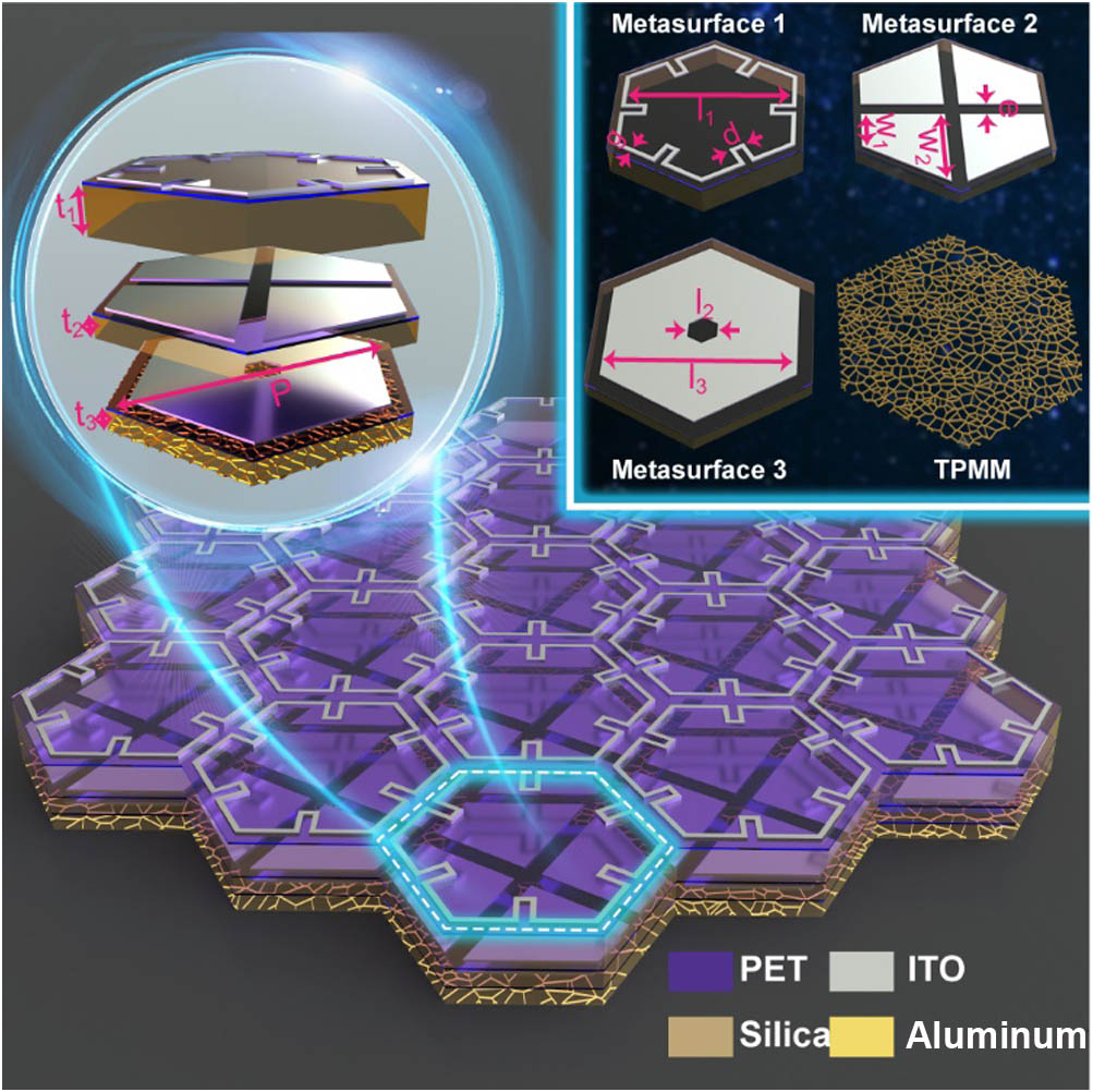
Fig. 1. Schematic diagram of the designed OTMMA. The geometrical parameters in the inset are t 1 = 2 mm t 2 = 1 mm t 3 = 1 mm p = 15 mm l 1 = 11.39 mm d = 1.1 mm w 1 = 3 mm w 2 = 6.21 mm g = 0.5 mm e = 1 mm l 2 = 1.73 mm l 3 = 11.26 mm
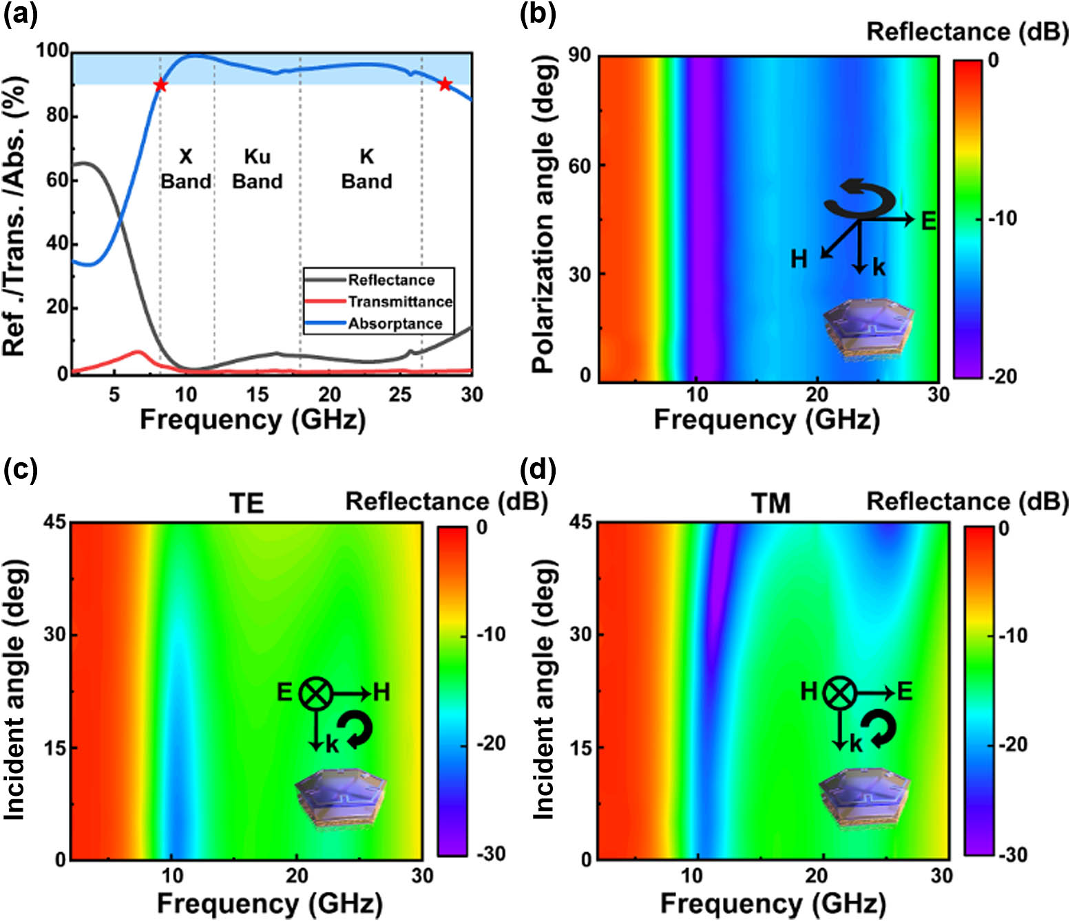
Fig. 2. Numerical results of a metamaterial absorber. (a) Reflectance/transmittance/absorptance spectra under normal incidence. (b) Reflectance over varied polarization angles under normal incidence. Reflectance over various incident angles under (c) TE-polarized and (d) TM-polarized waves.
Fig. 3. Generation process of the Thiessen polygon mesh. (a) Generation of random discrete points. (b) Generation of the Delaunay triangular mesh grid. (c) Generation of the circumcenter of each triangle. (d) Generation of the Thiessen polygon mesh grid.
Fig. 4. (a) Schematic diagram of an optical system with a mesh window. PSF of the optical system (b) without a metal mesh, (c) with a square metal mesh, and (d) with an OTMMA. Simulated MTF curves of the optical system with (e) 0° and (f) 5° FOVs, respectively. The wavelength of the incident light is 532 nm, the focal length is f = 200 mm
Fig. 5. (a) Micrograph of the fabricated TPMM; (b) and (c) scanning electron microscope (SEM) images of the TPMM.
Fig. 6. (a) Experimental setup for measuring reflectance. (b) Experimental setup for measuring SE. (c) Measured reflectance of the OTMMA under TE- and TM-polarized EM waves with the incidence angle ranging from 10° to 45°. (d) Measured SE of the OTMMA under TE- and TM-polarized EM waves.
Fig. 7. (a) Outdoor image of the fabricated OTMMA. (b) Measured optical transmittance of the OTMMA and quartz substrate.
Fig. 8. Schematic of an optical system with the OTMMA window.
Fig. 9. Schematic of micro pixel discretization of the metasurface and TPMM.
Fig. 10. Measured visible transmission of quartz with and without ITO film.
Fig. 11. (a), (b) and (c) Current distribution on metasurfaces 1, 2 and 3, respectively. (d), (e) and (f) Electric field on metasurfaces 1, 2, and 3, respectively.
Fig. 12. (a) Simulated reflectance of the OTMMA when surface resistance of the ITO metasurface is different. (b) Average absorptance of the OTMMA from 8 to 26.5 GHz versus surface resistance of the ITO metasurface.
Fig. 13. Equivalent circuit model of the OTMMA.
Fig. 14. Calculated input impedance of the OTMMA.


Set citation alerts for the article
Please enter your email address

© Copyright 2018-2021 | Chinese Laser Press. All Rights Reserved 沪ICP备15018463号-20