• Photonics Research
  • Vol. 11, Issue 7, 1354 (2023)
Naitao Song1、2、3, Qiao Sun1、2, Su Xu4、*, Dongzhi Shan1、2, Yang Tang1、2, Xiaoxi Tian1、2, Nianxi Xu1、2, and Jingsong Gao1、2、5
Author Affiliations
  • 1Key Laboratory of Optical System Advanced Manufacturing Technology, Changchun Institute of Optics, Fine Mechanics and Physics, Chinese Academy of Sciences, Changchun 130033, China
  • 2State Key Laboratory of Applied Optics, Changchun Institute of Optics, Fine Mechanics and Physics, Chinese Academy of Sciences, Changchun 130033, China
  • 3College of Da Heng, University of Chinese Academy of Sciences, Beijing 100049, China
  • 4State Key Laboratory of Integrated Optoelectronics, College of Electronic Science and Engineering, Jilin University, Changchun 130012, China
  • 5Jilin Provincial Key Laboratory of Advanced Optoelectronic Equipment and Instrument Manufacturing Technology, Changchun 130033, China
  • show less
    DOI: 10.1364/PRJ.486613 Cite this Article Set citation alerts
    Naitao Song, Qiao Sun, Su Xu, Dongzhi Shan, Yang Tang, Xiaoxi Tian, Nianxi Xu, Jingsong Gao. Ultrawide-band optically transparent antidiffraction metamaterial absorber with a Thiessen-polygon metal-mesh shielding layer[J]. Photonics Research, 2023, 11(7): 1354 Copy Citation Text show less

    Abstract

    Transparent absorbers, with a functional integration of broadband electromagnetic shielding, microwave camouflage, and optical transparency, have attracted increasing attention in the past decades. Metal mesh, an artificial, optically transparent, conducting material composed of periodic metallic gratings, is the optimal choice for the microwave shielding layer of transparent absorbers because of its excellent compatibility between high transparency and low resistance. However, the micrometer-level periodicity of metallic grating concentrates the diffraction of light, which degrades the imaging quality of cameras and sensors in common. In this study, we report on a generalized Thiessen-polygon-randomization method that prevents the concentration of the diffraction of light in periodic metallic grating and demonstrate an ultrawide-band optically transparent diffraction-immune metamaterial absorber. The absorber is constructed with a multilayer indium-tin-oxide-based metasurface and a Thiessen-polygon-randomized metal-mesh reflector. The lossy metasurface provides multimode absorption, whereas the Thiessen-polygon randomization prevents the concentration of the diffraction of light. The practical sample achieves a 10 dB absorptivity and shielding effectiveness over a range of 8–26.5 GHz, and the optical transparency is also preserved over the entire visible and near-infrared regions. The point spread function and field of view are both improved by using the antidiffraction absorber. Our study paves the way for the application of optically transparent electromagnetic devices, display, and optoelectronic integration in a more practical stage.

    1. INTRODUCTION

    Optically transparent microwave devices [1], which convey divergent microwave functionalities on optical observation windows, play important roles in the rapidly developing optoelectronic-integration compact systems for next-generation wireless communications [2], electromagnetic environmental safety [3], and hyperspectral detection [4]. Correspondingly, various types of optically transparent microwave devices have been developed in recent years, including antennas [5], sensors [6], wearable electronics [7], electrodes [8], and circuits [9].

    In contrast to conventional opaque microwave devices, the high-performance realization of transparent microwave devices relies on the outstanding transparent conducting materials [10]. Currently, there are several classes of transparent conducting materials: conducting polymers {e.g., poly(3,4-ethylenedioxy-thiophene) polystyrene sulfonate (PEDOT:PSS) [11]}, metals and metal oxides {e.g., indium tin oxide (ITO) [12]}, and carbon materials (e.g., graphene [10] and carbon nanotubes [13]). Among these, ITOs were the most popular transparent conducting materials owing to their low-cost and large-area fabrication [14]. Because the high optical transparency of ITOs is built at the cost of a nanometer-level thickness, the sheet resistance is not extremely low compared to that of pure metals [15]. Consequently, ITOs are usually selected for transparent microwave devices that do not strictly require low ohmic losses, e.g., transparent absorbers [14]. In particular, the intrinsic ohmic loss in ITOs (as well as other transparent conductors with considerable sheet resistance) broadens the working bandwidth of absorbers [16]. By using this property, various broadband transparent absorbers [12] have been demonstrated for their potential use for electromagnetic safety.

    Regarding practical electromagnetic safety, achieving only absorption is not sufficient. A high electromagnetic shielding effectiveness (SE) is another desired property in a practical scenario. For this purpose, a metal mesh with a lower sheet resistance has been considered to realize transparent absorptive shielding devices [17]. However, the periodicity of the metallic grating in a metal mesh generates a significant concentration of the diffraction of light, which deteriorates the quality of optical imaging [18]. This fundamental and common bottleneck critically constrains the practical application of optically transparent electromagnetic devices.

    In this study, we propose a generalized antidiffraction solution by using a Thiessen-polygon metal-mesh (TPMM) [19] metasurface in optically transparent microwave functional devices. As the proof of concept, we experimentally demonstrate an ultrawide-band optically transparent microwave metamaterial absorber (OTMMA) to reach the targets of preserving the critical figures of optical imaging and achieving broadband electromagnetic safety. The proposed absorber consists of tri-layer lossy ITO and quasi-perfect-reflective TPMM metasurfaces. This hybrid architecture achieved a 10-dB absorption and a 10-dB SE over a range of 8–26.5 GHz, and an average optical transparency of 84.3% was maintained over a wavelength range of 400–1200 nm. The point spread function (PSF) was improved by using an antidiffraction absorber.

    2. RESULTS AND DISCUSSION

    The schematic view of our OTMMA is illustrated in Fig. 1. The OTMMA consists of tri-layer ITO lossy metasurfaces and an aluminum mesh reflector. Quartz with a permittivity of 3.8 and loss tangent of 0.005 was used as the substrate to separate the individual lossy metasurfaces and the metal mesh. The thicknesses of the quartz layers were 2 mm, 1 mm, and 1 mm, from top to bottom. Each lossy metasurface was made from 23-nm-thick ITO (conductivity 2.89×10⁵  S/m) patterns on a 125-μm-thick PET (permittivity 3, loss tangent 0.06) substrate. Meta atoms of the tri-layer metasurface were snowflake-shaped, right-angle trapezoidal-shaped, and hexagonal holed resonators. We chose the hexagonal lattice so that more atoms can be arranged in the same area, which in turn enhances the broadband absorption properties of OTMMA. These resonators build circuitry loops on the lossy transmission line-modeled metasurface [12] and exhibit a strong absorption of electromagnetic power. Owing to various dimensions regarding the wavelengths of interest, the positions of absorption peaks can be tailored. Because the quality factor of resonance can be reduced with the intrinsic loss of circuits, the narrow absorptive peaks can be merged to a continuous and wide absorption band [16,20]. Numerical studies using CST Microwave Studio revealed excellent wideband absorptive performance of the OTMMA. An absorbance of more than 90% was achieved over a frequency band of 8.2–28.1 GHz, under the normal incidence of a plane wave linearly polarized along the x axis as shown in Fig. 2(a). The OTMMA also exhibited a good polarization insensitivity [Fig. 2(b)] and angular stability [Figs. 2(c) and 2(d)]. The polarization angle is defined as the angle between the direction of electric field vector and the x axis. Detailed theoretical analysis on the mechanism of the OTMMA can be found in Appendix B.

    Schematic diagram of the designed OTMMA. The geometrical parameters in the inset are t1 =2 mm, t2 =1 mm, t3 =1 mm, p=15 mm, l1 =11.39 mm, d=1.1 mm, w1 =3 mm, w2 =6.21 mm, g=0.5 mm, e=1 mm, l2 =1.73 mm, and l3 =11.26 mm.

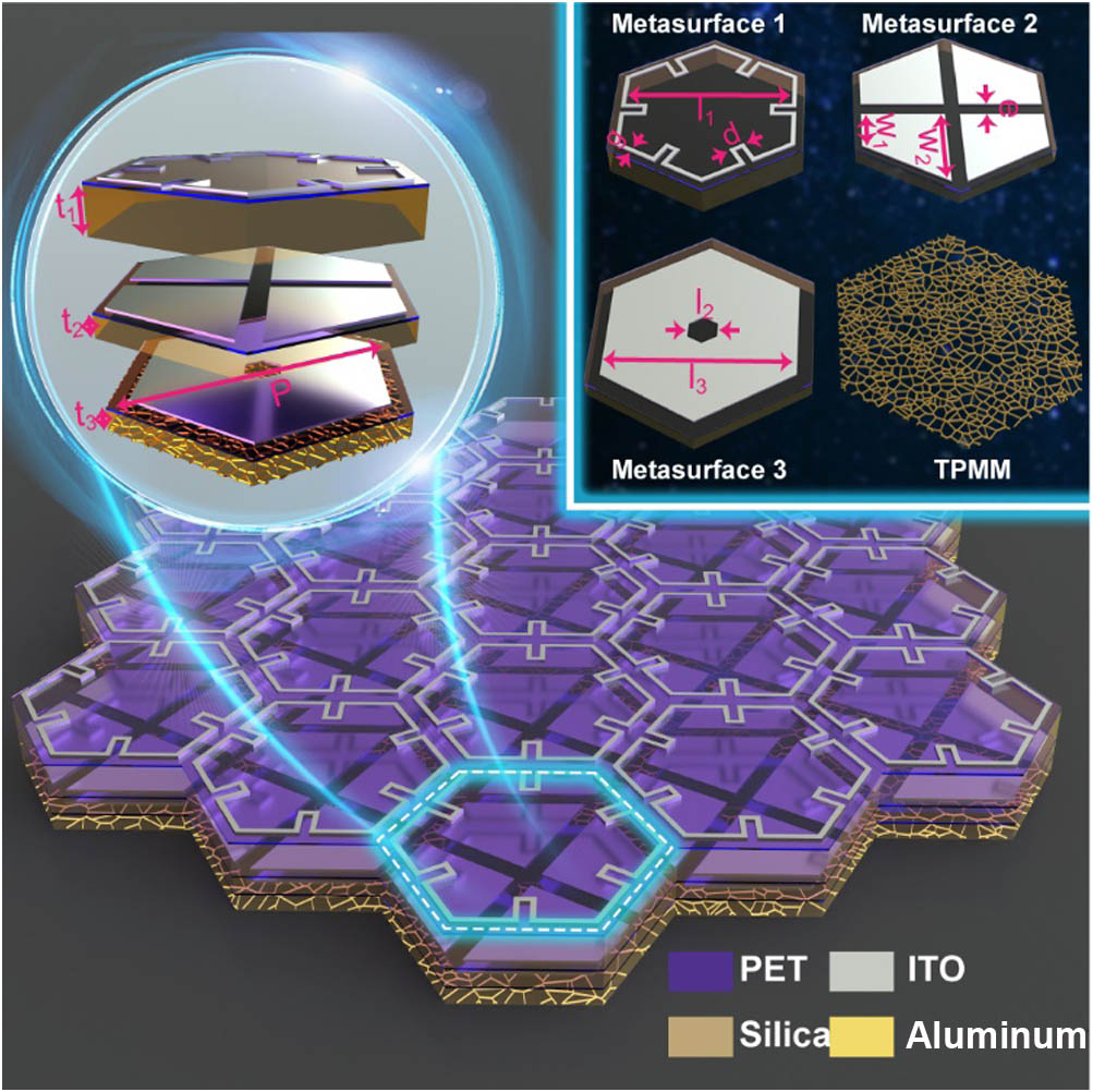
    Figure 1.Schematic diagram of the designed OTMMA. The geometrical parameters in the inset are t1=2  mm, t2=1  mm, t3=1  mm, p=15  mm, l1=11.39  mm, d=1.1  mm, w1=3  mm, w2=6.21  mm, g=0.5  mm, e=1  mm, l2=1.73  mm, and l3=11.26  mm.

    Numerical results of a metamaterial absorber. (a) Reflectance/transmittance/absorptance spectra under normal incidence. (b) Reflectance over varied polarization angles under normal incidence. Reflectance over various incident angles under (c) TE-polarized and (d) TM-polarized waves.

    Figure 2.Numerical results of a metamaterial absorber. (a) Reflectance/transmittance/absorptance spectra under normal incidence. (b) Reflectance over varied polarization angles under normal incidence. Reflectance over various incident angles under (c) TE-polarized and (d) TM-polarized waves.

    In our design, the metal mesh was used as the electromagnetic reflector to achieve both high optical transparency and high SE. The thickness, line width, and duty cycle were set to 500 nm, 6 μm, and 3.5%, respectively. To avoid the concentration of diffracted light that significantly degrades the imaging quality, Thiessen random polygons were introduced into the design of the metallic mesh. The inhomogeneity of the TPMM randomizes and homogenizes the stray light distribution, and thereby reduces the negative effect on the imaging quality [17]. The Thiessen polygons are generated in four steps as shown in Fig. 3. First, a series of random discrete points [blue points, Fig. 3(a)] are generated in the plane of the reflector. These discrete points are connected to form a Delaunay triangulation–based mesh grid [purple dashed line, Fig. 3(b)]. Then, the circumcenter [green pentagram, Fig. 3(c)] of each triangle is treated as the vertex of the polygon. Finally, these vertices are connected in turn to form the Thiessen polygon [yellow solid line, Fig. 3(d)]. Through this polygon-building process, both the periodicity and lattice angle of the metal mesh were randomized, and the interference due to lattice periods was broken such that the diffracted light intensity was distributed fairly uniformly.

    Generation process of the Thiessen polygon mesh. (a) Generation of random discrete points. (b) Generation of the Delaunay triangular mesh grid. (c) Generation of the circumcenter of each triangle. (d) Generation of the Thiessen polygon mesh grid.

    Figure 3.Generation process of the Thiessen polygon mesh. (a) Generation of random discrete points. (b) Generation of the Delaunay triangular mesh grid. (c) Generation of the circumcenter of each triangle. (d) Generation of the Thiessen polygon mesh grid.

    The antidiffraction performance of the Thiessen-polygon metal mesh was calculated by an optical system consisting of an OTMMA window, an ideal aberration-free lens, and a CCD, as shown in Fig. 4. The light field distribution on the CCD was calculated as detailed in Appendix A. With monochromatic incident light with amplitude A and phase φ0, the electric field distribution in the CCD plane is expressed as Ef(x,y)=Ajλfexp(jkf+φ0)exp[jk2f(1df)(x2+y2)]×F.T.[tOTMMA(x0,y0)]|fx=xλf,fy=yλf,where F.T. denotes a Fourier transform operator, d denotes the distance from the window to the lens, f is the focal length of the lens, and λ is the wavelength of the incident light. Figures 4(b)–4(d) show the intensity distribution for the cases of the CCD without the metal mesh, with the conventional square mesh, and with the OTMMA, respectively. Here, the intensity distribution on the CCD is also known as the PSF of the optical system under normal incidence. Without the metal mesh, the PSF of the optical system is an Airy disk, which indicates the ideal imaging quality. With the conventional square mesh, significant stray light spots appear in the axial direction on the PSF map due to a higher-diffraction-order light. Such highly concentrated strong stray light would generate a ghost image, which would degrade the imaging quality. For an optical system with an OTMMA window, the high-order diffracted energy is dispersed, and the background light intensity distribution is more uniform, which is favorable for an imaging system.

    (a) Schematic diagram of an optical system with a mesh window. PSF of the optical system (b) without a metal mesh, (c) with a square metal mesh, and (d) with an OTMMA. Simulated MTF curves of the optical system with (e) 0° and (f) 5° FOVs, respectively. The wavelength of the incident light is 532 nm, the focal length is f=200 mm, the distance from the window to the lens is 10 mm, and the aperture size of the optical system is 10 mm.

    Figure 4.(a) Schematic diagram of an optical system with a mesh window. PSF of the optical system (b) without a metal mesh, (c) with a square metal mesh, and (d) with an OTMMA. Simulated MTF curves of the optical system with (e) 0° and (f) 5° FOVs, respectively. The wavelength of the incident light is 532 nm, the focal length is f=200  mm, the distance from the window to the lens is 10 mm, and the aperture size of the optical system is 10 mm.

    Furthermore, the impacts of the OTMMA were evaluated quantitatively by using Zemax OpticStudio. The modulation transfer functions (MTFs) of this optical system with various fields of view (FOVs) are shown in Figs. 4(e) and 4(f). The MTFs at the Nyquist frequency decreased slightly with the TPMM for both normal and oblique incidences. The MTFs in the tangential and sagittal planes are consistent, indicating that astigmatism is not introduced in the optical system with the TPMM, and that the imaging quality is symmetric and uniform. The numerical results indicate that the randomness of the designed TPMM does not significantly degrade the imaging quality of the optical system.

    The TPMM, whose antidiffraction ability was confirmed, was fabricated through nano-imprinting technology. The micrograph of the fabricated TPMM is shown in Fig. 5, which reveals the integrity and connectivity of the metal mesh. In addition, SEM images of the TPMM are shown in Figs. 5(b) and 5(c) to exhibit the geometrical detail of the metallic mesh. We integrated the fabricated TPMM into the OTMMA shown in Fig. 1 to prove the potential application of the TPMM in optoelectronic integrated systems.

    (a) Micrograph of the fabricated TPMM; (b) and (c) scanning electron microscope (SEM) images of the TPMM.

    Figure 5.(a) Micrograph of the fabricated TPMM; (b) and (c) scanning electron microscope (SEM) images of the TPMM.

    To verify the performance of the practical OTMMA, reflectance, SE, and optical transmittance were experimentally measured. In the reflectance measurement, a pair of angular-movable horn antennas were placed on the arch to test the reflectance as shown in Fig. 6(a). As shown in Fig. 6(c), the reflectance of the OTMMA from 8 to 26.5 GHz was below 10  dB, revealing that the broadband absorption covers the entire X, Ku, and K bands for all incident angles and polarizations. For TE polarization, the reflectance increased as the incident angle increased, whereas for TM polarization, the reflectance decreased as the incident angle increased. This phenomenon is mainly related to the distinct impedance-changing trend for the cases of TE- and TM-polarized incidences. In the SE measurement, the receiving antenna was placed inside the anechoic box, the transmitting antenna was placed outside, and the OTMMA was fixed as the window of the anechoic box as shown in Fig. 6(b). Figure 6(d) shows the measured SE under TE and TM incidences. The SE of the OTMMA was above 10 dB from 6 to 26.5 GHz, which is mainly due to the strong absorptance of lossy metasurfaces and high reflectance of the TPMM.

    (a) Experimental setup for measuring reflectance. (b) Experimental setup for measuring SE. (c) Measured reflectance of the OTMMA under TE- and TM-polarized EM waves with the incidence angle ranging from 10° to 45°. (d) Measured SE of the OTMMA under TE- and TM-polarized EM waves.

    Figure 6.(a) Experimental setup for measuring reflectance. (b) Experimental setup for measuring SE. (c) Measured reflectance of the OTMMA under TE- and TM-polarized EM waves with the incidence angle ranging from 10° to 45°. (d) Measured SE of the OTMMA under TE- and TM-polarized EM waves.

    Figure 7(a) shows an outdoor image of the OTMMA with a colored background, which indicates the good transparency of the OTMMA. The optical transmittance of the OTMMA was measured quantitatively with a UV/visible/NIR spectrometer (Lambda 1050, PerkinElmer, USA), and the results are shown in Fig. 7(b). The average transmittances of the OTMMA over the visible and NIR regions were 81.2% and 86.7%, respectively. Therefore, the OTMMA can be used as a window for optical systems working at visible and NIR wavelengths.

    (a) Outdoor image of the fabricated OTMMA. (b) Measured optical transmittance of the OTMMA and quartz substrate.

    Figure 7.(a) Outdoor image of the fabricated OTMMA. (b) Measured optical transmittance of the OTMMA and quartz substrate.

    3. CONCLUSION

    We proposed an antidiffraction TPMM with strong microwave shielding and high optical transparency as a method of preventing the concentration of stray light and minimizing the degrading impact on the imaging quality for optically transparent electromagnetic devices. As the proof of concept, a functional EM-device OTMMA was experimentally demonstrated. The experimental results revealed that both absorptance and SE were above 10 dB from 8 to 26.5 GHz, while an average optical transparency of 84.3% was maintained over wavelengths ranging from 400 to 1200 nm. Moreover, the OTMMA exhibited good angular stability and polarization insensitivity. Our study paves the way for further research on optically transparent functional EM devices, multispectral integrated detection systems, and transparent displays.

    APPENDIX A: ANALYSIS OF IMAGING QUALITY OF OPTICAL SYSTEMS WITH OTMMA WINDOWS

    We use Fresnel–Huygens diffraction theory to analyze the impact of the OTMMA on the imaging quality of the optical system, which is shown in Fig. 8.

    Schematic of an optical system with the OTMMA window.

    Figure 8.Schematic of an optical system with the OTMMA window.

    Schematic of micro pixel discretization of the metasurface and TPMM.

    Figure 9.Schematic of micro pixel discretization of the metasurface and TPMM.

    Measured visible transmission of quartz with and without ITO film.

    Figure 10.Measured visible transmission of quartz with and without ITO film.

    We assume that the incident light is a monochromatic plane wave with an amplitude of A and phase of φ0. The electric field of light passing through the OTMMA window can be expressed as [21] E0(x0,y0)=AtOTMMA(x0,y0)exp(jφ0).

    Here the reflections caused by the windows are ignored, and without loss of generality, we assume that the amplitude is 1 and the initial phase is 0. A=1,φ0=0.

    The shift of the phase introduced by the lens can be expressed as tlen(ε,μ)=exp[jk2f(ε2+μ2)]P(ε,μ),where P(ε,μ) is the aperture function of the lens, ε and μ are the coordinates where thin lens is located, and since the distance between window and lens is much smaller than the focal length of the lens, we can ignore the finite aperture size of the lens.P(ε,μ)=1.

    We use Fresnel diffraction integral to calculate the field on a CCD. Ef(x,y)=1jkfexp[jk2f(x2+y2)]×E2(ε,μ)exp[jk2f(ε2+μ2)]exp[j2πλf(xε+yμ)]dεdμ,where k is the wavenumber in the vacuum, λ is the wavelength in the vacuum, and E2(ε,μ) is the electric field after light passes through the lens. E2(ε,μ)=E1(ε,μ)tlen(ε,μ).

    Substituting Eq. (A6) and Eq. (A9) into Eq. (A8), we obtain Ef(x,y)=1jkfexp[jk2f(x2+y2)]×E1(ε,μ)tlens(ε,μ)exp[jk2f(ε2+μ2)]exp[j2πλf(xε+yμ)]dεdμ=1jkfexp[jk2f(x2+y2)]×E1(ε,μ)exp[j2πλf(xε+yμ)]dεdμ=1jkfexp[jk2f(x2+y2)]×F.T.[E1(ε,μ)]|fx=xλf,fy=yλf,where F.T. [E1(ε,μ)] is the Fourier transform of E1(ε,μ), and E1(ε,μ) is electric field before light passing through the lens. According to the angular spectrum diffraction theory, E1(ε,μ) can be expressed as F.T.[E1(ε,μ)]=F.T.[E0(x0,y0)]T(fx,fy),where T(fx,fy) is the Fresnel transfer function, T(fx,fy)=exp[jπλd(fx2+fy2)].

    Substituting Eqs. (A11) and (A12) into Eq. (A10), we can get the light field distribution on the CCD plane. Ef(x,y)=1jkfexp[jk2f(x2+y2)]exp[jπλd(fx2+fy2)]×F.T.[E0(x0,y0)]|fx=xλf,fy=yλf=1jkfexp[jk2f(x2+y2)]exp{jπλd[(xλf)2+(yλf)2]}×F.T.[E0(x0,y0)]|fx=xλf,fy=yλf=1jλfexp(jkf)exp[jk2f(1df)(x2+y2)]×F.T.[tOTMMA(x0,y0)]|fx=xλf,fy=yλf.

    The intensity distribution on the CCD, also known as the point spread function of the optical system under normal incidence, is an important metric to evaluate the imaging quality of an optical system.

    APPENDIX B: THEORETICAL ANALYSIS OF ABSORPTION PERFORMANCE OF THE OTMMA

    Capacitively coupled electric dipole resonances are excited on each layer of metasurfaces to enhance the absorption of EM waves. For example, for metasurface 1, the electric dipole resonance will be excited when the circumference of the curled hexagon is equal to the wavelength of the incident wave as shown in Fig. 11(a). Since the geometry of each metasurface layer is different, each metasurface layer can resonate at different wavelengths and enhance the absorption of EM waves at different wavelengths, respectively. In addition, by adjusting the surface resistance, we can regulate the quality factor of the resonance as shown in Fig. 12(a), and finally all resonances are merged to form a broadband microwave absorption. This is the physical mechanism by which three-layer lossy metasurfaces can efficiently absorb EM waves in a broadband.

    (a), (b) and (c) Current distribution on metasurfaces 1, 2 and 3, respectively. (d), (e) and (f) Electric field on metasurfaces 1, 2, and 3, respectively.

    Figure 11.(a), (b) and (c) Current distribution on metasurfaces 1, 2 and 3, respectively. (d), (e) and (f) Electric field on metasurfaces 1, 2, and 3, respectively.

    (a) Simulated reflectance of the OTMMA when surface resistance of the ITO metasurface is different. (b) Average absorptance of the OTMMA from 8 to 26.5 GHz versus surface resistance of the ITO metasurface.

    Figure 12.(a) Simulated reflectance of the OTMMA when surface resistance of the ITO metasurface is different. (b) Average absorptance of the OTMMA from 8 to 26.5 GHz versus surface resistance of the ITO metasurface.

    Equivalent circuit model of the OTMMA.

    Figure 13.Equivalent circuit model of the OTMMA.

    Calculated input impedance of the OTMMA.

    Figure 14.Calculated input impedance of the OTMMA.

    The impedance of each metasurface is also determined by its surface resistance. As shown in Fig. 12(a), the absorption bandwidth becomes larger as the surface resistance increases. Although we expect the absorption bandwidth to become wider and wider, the strength of the absorption decreases when the resistance becomes large to a certain extent. Therefore, we have to trade off the absorption strength and the absorption bandwidth. As shown in Fig. 12(b), the surface resistance of the metasurface is chosen to be 150  Ω/ in this paper to achieve the highest average absorption.

    References

    [1] M. Green, Z. Liu, P. Xiang, Y. Liu, M. Zhou, X. Tan, F. Huang, L. Liu, X. Chen. Doped, conductive SiO2 nanoparticles for large microwave absorption. Light Sci. Appl., 7, 87(2018).

    [2] L. Li, P. Zhang, F. Cheng, M. Chang, T. J. Cui. An optically transparent near-field focusing metasurface. IEEE Trans. Microw. Theory Tech., 69, 2015-2027(2021).

    [3] D. Kitayama, Y. Hama, K. Goto, K. Miyachi, T. Motegi, O. Kagaya. Transparent dynamic metasurface for a visually unaffected reconfigurable intelligent surface: controlling transmission/reflection and making a window into an RF lens. Opt. Express, 29, 29292-29307(2021).

    [4] D. Li, Q. Chen, J. Huang, H. Xu, Y. Lu, W. Song. Scalable-manufactured metamaterials for simultaneous visible transmission, infrared reflection, and microwave absorption. ACS Appl. Mater. Interfaces, 14, 33933-33943(2022).

    [5] R. N. Simons, R. Q. Lee. Feasibility study of optically transparent microstrip patch antenna. IEEE Antennas and Propagation Society International Symposium, 2100-2103(1997).

    [6] P. Won, K. K. Kim, H. Kim, J. J. Park, I. Ha, J. Shin, J. Jung, H. Cho, J. Kwon, H. Lee, S. H. Ko. Transparent soft actuators/sensors and camouflage skins for imperceptible soft robotics. Adv. Mater., 33, 2002397(2021).

    [7] K. Ellmer. Past achievements and future challenges in the development of optically transparent electrodes. Nat. Photonics, 6, 809-817(2012).

    [8] K. Mitsubayashi, Y. Wakabayashi, S. Tanimoto, D. Murotomi, T. Endo. Optical-transparent and flexible glucose sensor with ITO electrode. Biosens. Bioelectron., 19, 67-71(2003).

    [9] S. Kim, S. Kim, J. Park, S. Ju, S. Mohammadi. Fully transparent pixel circuits driven by random network carbon nanotube transistor circuitry. ACS Nano, 4, 2994-2998(2010).

    [10] L. Ma, H. Xu, Z. Lu, J. Tan. Optically transparent broadband microwave absorber by graphene and metallic rings. ACS Appl. Mater. Interfaces, 14, 17727-17738(2022).

    [11] H. Shi, C. Liu, Q. Jiang, J. Xu. Effective approaches to improve the electrical conductivity of PEDOT:PSS: a review. Adv. Electron. Mater., 1, 1500017(2015).

    [12] H. Li, H. Dong, Y. Zhang, N. Mou, Y. Xin, R. Deng, L. Zhang. Transparent ultra-wideband double-resonance-layer metamaterial absorber designed by a semiempirical optimization method. Opt. Express, 29, 18446-18457(2021).

    [13] S. K. Singh, M. J. Akhtar, K. K. Kar. Hierarchical carbon nanotube-coated carbon fiber: ultra lightweight, thin, and highly efficient microwave absorber. ACS Appl. Mater. Interfaces, 10, 24816-24828(2018).

    [14] Y. Xiong, F. Chen, Y. Cheng, H. Luo. Rational design and fabrication of optically transparent broadband microwave absorber with multilayer structure based on indium tin oxide. J. Alloys Compd., 920, 166008(2022).

    [15] R. Deng, K. Zhang, M. Li, L. Song, T. Zhang. Targeted design, analysis and experimental characterization of flexible microwave absorber for window application. Mater. Des., 162, 119-129(2019).

    [16] C. Zhang, Q. Cheng, J. Yang, J. Zhao, T. J. Cui. Broadband metamaterial for optical transparency and microwave absorption. Appl. Phys. Lett., 110, 143511(2017).

    [17] H. Zhong, Y. Han, J. Lin, P. Jin. Pattern randomization: an efficient way to design high-performance metallic meshes with uniform stray light for EMI shielding. Opt. Express, 28, 7008-7017(2020).

    [18] H. Wang, Z. Lu, Y. Liu, J. Tan, L. Ma, S. Lin. Double-layer interlaced nested multi-ring array metallic mesh for high-performance transparent electromagnetic interference shielding. Opt. Lett., 42, 1620-1623(2017).

    [19] K. E. Brassel, D. Reif. A procedure to generate Thiessen polygons. Geogr. Anal., 11, 289-303(1979).

    [20] T. Jang, H. Youn, Y. J. Shin, L. J. Guo. Transparent and flexible polarization-independent microwave broadband absorber. ACS Photon., 1, 279-284(2014).

    [21] J. W. Goodman. Introduction to Fourier Optics(2005).

    Naitao Song, Qiao Sun, Su Xu, Dongzhi Shan, Yang Tang, Xiaoxi Tian, Nianxi Xu, Jingsong Gao. Ultrawide-band optically transparent antidiffraction metamaterial absorber with a Thiessen-polygon metal-mesh shielding layer[J]. Photonics Research, 2023, 11(7): 1354
    Download Citation