Amged Alquliah, Mohamed Elkabbash, Jinluo Cheng, Gopal Verma, Chaudry Sajed Saraj, Wei Li, Chunlei Guo, "Reconfigurable metasurface-based 1 × 2 waveguide switch," Photonics Res. 9, 2104 (2021)

Search by keywords or author
- Photonics Research
- Vol. 9, Issue 10, 2104 (2021)

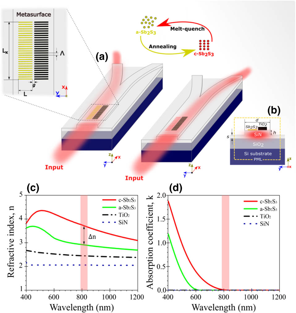
Fig. 1. Design of the proposed metasurface-based reconfigurable (1 × 2 ) integrated switch working around λ = 800 nm . (a) 3D illustrations of the device structure and its functionality when the Sb 2 S 3 metasurface structure is in a crystalline or amorphous state. The top-left inset shows the top view of the device with dimensions of the metasurface consisting of a set of passive TiO 2 nanorods and another set of PCM (Sb 2 S 3 ) nanorods. The top middle inset shows the conditions required for the Sb 2 S 3 to undergo a reversible structural transition from amorphous to crystalline states. (b) Cross section of the device. (c) and (d) Wavelength dependence of the complex optical constants (n , k ) of amorphous Sb 2 S 3 , crystalline Sb 2 S 3 , amorphous titanium dioxide, and silicon nitride. Highlighted parts in red indicate the spectral region of interest where Sb 2 S 3 exhibits low loss and high switching contrast.

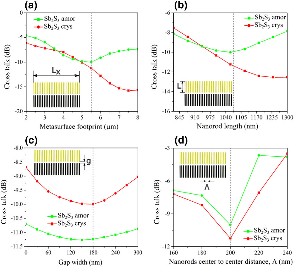
Fig. 2. Metasurface parametric sweep. (a)–(d) Device cross talk as a function of metasurface footprint (L x ), nanorod length (L ), separated gap width (g ), and the nanorods’ center-to-center distance (Λ ), respectively, for a - Sb 2 S 3 and c - Sb 2 S 3 . The dotted gray lines show the dimensions used in our metasurface.

Fig. 3. Characterization of nanoantenna structure. (a) Profile (zy plane) of the normalized near field of the E z component showing scattering Mie modes in the TiO 2 and Sb 2 S 3 nanoantennas for a - Sb 2 S 3 (left panel) and c - Sb 2 S 3 (right panel) at λ = 800 nm . (b) Normalized electric field intensity | E | 2 distribution (zy plane) in the same nanorods for a - Sb 2 S 3 and c - Sb 2 S 3 . The boundaries of the SiN waveguide and nanoantennas are indicated in solid black lines. (c) Effective refractive index of the TE 00 mode as a function of TiO 2 nanoantenna length and Sb 2 S 3 nanoantenna length for the a - Sb 2 S 3 and c - Sb 2 S 3 phases. The dashed gray line indicates the length of the nanorods (L ) used in our simulation. The inset figure shows the FDE simulation setup.

Fig. 4. Simulated device performance for a - Sb 2 S 3 (upper panel) and c - Sb 2 S 3 (lower panel). (a) and (d) Full-wave simulation showing the optical field intensity | E | 2 in the switch for the fundamental TE mode in the xy plane at λ = 800 nm . The boundaries of the SiN waveguide and metasurface structure are indicated by dashed lines and rectangles, respectively. Inset: enlarged view of the field profile in the metasurface. (b) and (e) Transmission spectra at two output ports Port 2 and Port 3 . (c) and (f) Total transmission at output ports (Port 2 + Port 3 ), reflection, and scattering of the device.

Fig. 5. Multimode waveguide characterization. The dependence of waveguide width on the (a) n eff and (b) dispersion D of different SiN waveguide modes at λ = 800 nm . The shaded region indicates the waveguide widths that support asymmetric multimode. The dashed black lines show the maximal modal index (n eff ) in the waveguide and the waveguide width that support a single mode. The gray dotted line indicates the width considered in the stem SiN waveguide. (c) n eff and D of the fundamental TE 00 mode as a function of simulated wavelengths. The inset figure shows the E y distribution of the TE 00 mode at λ = 800 nm .

Fig. 6. Parametric sweep of TiO 2 nanorods for the TE 00 mode at λ = 800 nm . (a) and (b) Simulated device cross talk considering variations of the height and width of TiO 2 nanorods when Sb 2 S 3 is in the crystalline and amorphous state, respectively. (c) and (d) Calculated transmission at the desired output as a function of height and width of TiO 2 nanorods for the crystalline and amorphous state, respectively. The black dashed lines indicate the dimensions used in our metasurface.

Fig. 7. Full-wave simulation showing the optical field intensity | E | 2 in the switch for the fundamental TE mode in the xy plane at λ = 800 nm and for different TiO2 dimensions for (a)–(c) c - Sb 2 S 3 and (d)–(f) a - Sb 2 S 3 , The boundaries of the SiN waveguide and metasurface structure are indicated by dashed lines and rectangles, respectively. Inset: enlarged view of the field profile in the metasurface.

Fig. 8. Suggested fabrication method employing three steps of electron beam lithography: (a) two positive resists followed by LPCVD to transfer the desired patterns of the nanorod arrays onto the developed gaps and (b) a negative resist followed by reactive ion etching (RIE) to define the SiN waveguide.

Fig. 9. Device fabrication tolerance. (a) and (b) Simulated device cross talk for the fundamental mode operating at λ = 800 nm , considering possible parallel misalignment (offset) and axial misalignment (gap width), respectively. The gray dotted lines in the figures indicate the dimensions used in our device.

Fig. 10. Schematic illustration of the experimental setup suggested for characterizing the performance of the proposed reconfigurable switch. Here, PPG is a programmable pulse generator, PC is a power controller, and M is a mirror.

Fig. 11. Sketches showing x -periodic Sb 2 S 3 and TiO 2 nanoantennas patterned on a SiN waveguide in (a) xy plane and (b), (c) zy plane, where n a / c are the effective indices of a - Sb 2 S 3 and c - Sb 2 S 3 nanorods, n 2 is the effective index of the TiO 2 nanorods, and n bare is the effective index of bare SiN waveguide. (d) Effective refractive indices for the waveguide cross section calculated using FDE. The inset shows the FDE simulation setup. (e) Effective indices for nanorod arrays calculated by Rytov’s approximation.

Fig. 12. Modes in the input and output ports of SiN waveguides. Simulated Ey component at λ = 800 nm for the TE 00 mode in the (a) input stem SiN waveguide before interacting with the metasurface, (b) output Port 3 for a - Sb 2 S 3 and (c) output Port 2 for c - Sb 2 S 3 . The arrows indicate the vector diagrams of the electric field component of the modes. The dashed black lines show the boundaries of the SiN waveguides.
|
Table 1. Comparison of Previously Reported PCM-Based (1 × 2 ) Switches with Our Metasurface-Based Switch

Set citation alerts for the article
Please enter your email address