• Photonics Research
  • Vol. 9, Issue 10, 2104 (2021)
Amged Alquliah1、2, Mohamed Elkabbash3、4、5、*, Jinluo Cheng1、2、6、*, Gopal Verma1、2, Chaudry Sajed Saraj1、2, Wei Li1、2、7、*, and Chunlei Guo3、8、*
Author Affiliations
  • 1GPL, Changchun Institute of Optics, Fine Mechanics and Physics, Chinese Academy of Sciences, Changchun 130033, China
  • 2University of Chinese Academy of Sciences, Beijing 100049, China
  • 3The Institute of Optics, University of Rochester, Rochester, New York 14627, USA
  • 4Current address: The Research Laboratory of Electronics, Massachusetts Institute of Technology, Cambridge, Massachusetts 02139, USA
  • 5e-mail: melkabba@mit.edu
  • 6e-mail: jlcheng@ciomp.ac.cn
  • 7e-mail: weili1@ciomp.ac.cn
  • 8e-mail: guo@optics.rochester.edu
  • show less
    DOI: 10.1364/PRJ.428577 Cite this Article Set citation alerts
    Amged Alquliah, Mohamed Elkabbash, Jinluo Cheng, Gopal Verma, Chaudry Sajed Saraj, Wei Li, Chunlei Guo. Reconfigurable metasurface-based 1 × 2 waveguide switch[J]. Photonics Research, 2021, 9(10): 2104 Copy Citation Text show less

    Abstract

    Reconfigurable nanophotonic components are essential elements in realizing complex and highly integrated photonic circuits. Here we report a novel concept for devices with functionality to dynamically control guided light in the near-visible spectral range, which is illustrated by a reconfigurable and non-volatile (1×2) switch using an ultracompact active metasurface. The switch is made of two sets of nanorod arrays of TiO2 and antimony trisulfide (Sb2S3), a low-loss phase-change material (PCM), patterned on a silicon nitride waveguide. The metasurface creates an effective multimode interferometer that forms an image of the input mode at the end of the stem waveguide and routes this image toward one of the output ports depending on the phase of PCM nanorods. Remarkably, our metasurface-based 1×2 switch enjoys an ultracompact coupling length of 5.5 μm and a record high bandwidth (22.6 THz) compared to other PCM-based switches. Furthermore, our device exhibits low losses in the near-visible region (1 dB) and low cross talk (-11.24 dB) over a wide bandwidth (22.6 THz). Our proposed device paves the way toward realizing compact and efficient waveguide routers and switches for applications in quantum computing, neuromorphic photonic networking, and biomedical sensing and optogenetics.

    1. INTRODUCTION

    The advancement of nanofabrication, coupled with the attainment of a high level of complexity in photonic integrated circuits (PICs), triggered tremendous interest toward realizing miniaturized all-optical interconnects that are superior to electronic circuits in terms of bandwidth density, speed, and energy efficiency as well as mitigating the von Neumann data transmission bottleneck [13]. Particularly, the reconfigurable control of light propagating in PICs is crucially important for many emerging applications such as programmable PIC [4], neuro-inspired computing [5,6], quantum information processing [7,8], optical communication [9,10], microwave photonics [11], and sensor applications [12,13].

    Reconfigurable photonic computing cores are conventionally implemented using waveguide meshes of Mach–Zehnder interferometers (MZIs) where the interference is controlled via two phase shifters that are independently tuned through volatile and weak modulation of the waveguide refractive index commonly using electro-optic or thermo-optic effects [4], leading to devices with a limited tunability, high energy consumption [several milliwatts (mW)], and large footprints [hundreds of micrometers (μm)] [14]. On the other hand, micro-ring resonators (MRRs) [1520] and micro-electromechanical systems (MEMS) [21,22] offer high modulation depth and a relatively small footprint. Still, they suffer from a narrow operational bandwidth (less than 3 dB) [20], low tolerance to temperature variations and fabrication errors, as well as a large actuation voltage (>40  V) [23]. Notably, systems based on exciting surface plasmon resonances (SPRs) enjoy the highest switching rates and smallest footprints. However, they suffer from high insertion and propagation losses as they require coupling from/to a photonic waveguide [24,25], and plasmonic metals are highly lossy [25], which hinder their widespread usage. The common volatility of these schemes necessitates an “always-on” power supply to retain the switching state, rendering them energy inefficient [14,26].

    To circumvent these hurdles, phase-change materials (PCMs) emerged as candidates to demonstrate photonic reconfigurability owing to their unique tunable properties [27,28]. PCMs possess high contrasts in the electrical resistivity and refractive index between the resonant-bonded crystalline and covalent-bonded amorphous phase states over a wide spectral range. They are non-volatile, reversible, and they provide fast and low energy actuation (<10  aJ/nm3 [29]) by ultrashort electrical or optical pulses (up to subnanosecond) [30] and stable switching ability of more than 1015 cycles [31]. In addition, the scalability of PCMs makes their nanofabrication relatively approachable and compatible with other substrates, as their amorphous state is used during deposition [23]. Several PCM-based integrated photonic devices were recently demonstrated, e.g.,  photonic memories [32,33], optical modulators [34,35], optical switches [1420], and optical computing [36,37]. In these applications, a top-cladding layer of Ge2Sb2Te5 (GST) and, recently, Ge2Sb2Se4Te1 (GSST) was deposited onto a waveguide. However, the high absorption losses in one of the phases of such materials fundamentally restrict their use in phase modulation schemes for large-area PICs [4] and deep-neural networks [5,6], where light would propagate through several PCM-based interconnects. Although losses can be alleviated in devices working at the telecom wavelengths, this comes with the cost of sacrificing the device footprint. In addition, such approach is impractical at the visible and near-visible wavelengths due to the large intrinsic losses. Finally, the use of large-area PCMs creates a considerable barrier to the actuation mechanism (see Appendix A for more details).

    On the other hand, optical metasurfaces enable unprecedented flexibility in controlling the propagation of light through a spatially dependent and abrupt phase change at an interface that is imposed by ultrathin artificial arrays of engineered subwavelength nanoantennas [38]. Metasurfaces have realized a plethora of ultracompact, broadband, and efficient on-chip photonic devices, such as mode converters [39], polarization rotators [39], mode-pass polarizers [40], power splitters [41], asymmetric power transmitters [39], second-harmonic generators [42], remote near-field controllers [43], and guided waves to free space wave couplers [4446]. However, these devices are passive and application specific because the optical properties of the constitutional meta-atoms are permanent once fabricated. To actively tune the optical properties of metasurfaces, several approaches have been introduced [47,48] with considerable interest in using PCMs [28,49] due to their advantages as discussed above. So far, such investigations on reconfigurable metasurfaces are focusing on controlling light propagating in free space, e.g.,  for bichromatic and multifocus Fresnel zone plates [50], beam steering [31], tunable color generators [51], dynamic spectrum controllers [52], switchable spectral filters [53], information processing [54], communication [55], imaging [56], hologram and augmented reality [5759], vortex beam generators, and illusion and cloaking [60].

    In this paper, we extend the concept of reconfigurable metasurfaces to PICs by reporting a novel dynamic near-visible nanophotonic (1×2) switch enabled by combining two nanorod arrays of TiO2 and a novel ultralow-loss PCM (antimony trisulfide Sb2S3) superimposed on silicon nitride waveguide. Our designed device provides unprecedented functionality as it facilitates the non-volatile dynamic routing of light inside a multimode waveguide toward predefined outputs. The device shows a wide bandwidth of 22.6 THz, low loss (1  dB), and low cross talk (<11.29  dB) with a compact active length (5.5 μm). To the extent of our knowledge, our design enjoys a record footprint compared to PCM-based optical switches, which would overcome the challenges associated with large-area PCM actuation. Table 1 compares the design principles, the type of PCM designs, and performance of the reported (1×2) PCM-based switches and of our metasurface PCM-based switch. Appendix B discusses the need for visible/near-visible PICs.

    Comparison of Previously Reported PCM-Based (1×2) Switches with Our Metasurface-Based Switch

    Design PrinciplePCM DesignBandwidth (THz)Cross Talk (dB)Operating Wavelength RangeReference
    Directional couplerGST layer3.7410IR[14]
    Directional couplerGSST layer4.432IR[61]
    Contra-directional couplerGST-Si grating0.27530IR[62]
    Micro-ring resonatorGST layer0.1256IR[16]
    Micro-ring resonatorGST layer0.12533IR[17]
    Micro-ring resonatorGST layer0.12542IR[18]
    Micro-ring resonatorGST layer0.1255IR[15]
    Micro-ring resonatorGST nanodisk0.1255IR[20]
    Micro-ring resonatorGST layer0.12514.1IR[19]
    Micro-ring resonatorSb2S3 layer0.125NAVisible[63]
    Y branchSb2S3/TiO2metasurface22.611.24Near visibleThis work

    2. MATERIALS AND METHODS

    Figure 1(a) schematically illustrates the structure and functionality of our device, which is a Y-branch waveguide with a metasurface located on the surface of its stem. From bottom to top, the waveguide is formed by a silicon substrate, a 3 μm thick SiO2 layer, and a ridge SiN waveguide. The metasurface consists of two sets of nanorods. Each set includes 28 equally spaced nanorods with a length L and a center-to-center distance between neighbor nanorods Λ. These two sets are aligned to form two adjacent rectangles separated by a gap g. The total footprint of the metasurface is Lx.

    Design of the proposed metasurface-based reconfigurable (1×2) integrated switch working around λ=800 nm. (a) 3D illustrations of the device structure and its functionality when the Sb2S3 metasurface structure is in a crystalline or amorphous state. The top-left inset shows the top view of the device with dimensions of the metasurface consisting of a set of passive TiO2 nanorods and another set of PCM (Sb2S3) nanorods. The top middle inset shows the conditions required for the Sb2S3 to undergo a reversible structural transition from amorphous to crystalline states. (b) Cross section of the device. (c) and (d) Wavelength dependence of the complex optical constants (n, k) of amorphous Sb2S3, crystalline Sb2S3, amorphous titanium dioxide, and silicon nitride. Highlighted parts in red indicate the spectral region of interest where Sb2S3 exhibits low loss and high switching contrast.

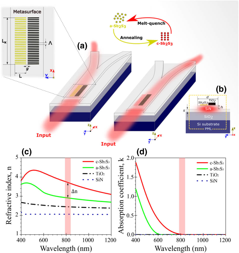
    Figure 1.Design of the proposed metasurface-based reconfigurable (1×2) integrated switch working around λ=800  nm. (a) 3D illustrations of the device structure and its functionality when the Sb2S3 metasurface structure is in a crystalline or amorphous state. The top-left inset shows the top view of the device with dimensions of the metasurface consisting of a set of passive TiO2 nanorods and another set of PCM (Sb2S3) nanorods. The top middle inset shows the conditions required for the Sb2S3 to undergo a reversible structural transition from amorphous to crystalline states. (b) Cross section of the device. (c) and (d) Wavelength dependence of the complex optical constants (n, k) of amorphous Sb2S3, crystalline Sb2S3, amorphous titanium dioxide, and silicon nitride. Highlighted parts in red indicate the spectral region of interest where Sb2S3 exhibits low loss and high switching contrast.

    The materials are chosen to realize a device appropriate for near-visible integrated photonics. The SiN waveguide has the advantages of thermodynamic stability, wide spectral range of transparency (λ=0.258  μm), higher fabrication flexibility, and lower propagation losses compared to silicon waveguides [64]. The materials of the two sets of nanorods are chosen as PCM antimony trisulfide (Sb2S3) for one set and amorphous titanium dioxide (a-TiO2) for the other. Compared to the prototypical PCM (GST), the new class of PCM (Sb2S3) has a bandgap tunable from 2.0 eV (crystalline) to 1.7 eV (amorphous), and thus it works in the near-visible spectrum with a low absorption coefficient and a relatively higher contrast in the change of the real part of its refractive index Δn [6567]. A-TiO2 is chosen because it is lossless in the near-visible range and enjoys a high refractive index to provide strong guided light–nanorod interaction [68]. The top middle inset in Fig. 1(a) shows the reversible optical switching of the Sb2S3 from the crystalline to amorphous phases. The optical switching [6567] can be done using a 630 nm laser source with a power of up to 90 mW. This laser source provides stable performance and cycling durability of Sb2S3 during the experiment [67]. The reversible switching between both structural states of Sb2S3 is realized by controlling the width and focus of the laser pulse [67]. The crystallization process requires pulses with long time duration (100 ms) [67] to reach the Sb2S3 glass transition temperature at 270°C [67]. In contrast, the re-amorphization process requires pulses with shorter time duration (400 ns) [67] to reach the Sb2S3 melting temperature at 527.85°C [67] and then quickly cool it at a rate >20°C/ns [53,67,69].

    In our designed metasurface, the nanorod antennas cause a spatial linear phase shift of the optical mode in the waveguide in addition to the propagation phase along the propagation direction (x axis). The accumulative local phase shifts from the two nanorod sets result in a constructive interference that focuses the input fundamental mode in the stem multimode waveguide. Following that, the focused input mode partially converts the input fundamental mode to higher-order modes, creating an effective asymmetric multimode interferometer (MMI). Consequently, an image of the input mode is formed at the end of the stem multimode waveguide due to the self-imaging principle of the MMI [70]. The produced image is then routed in one of the predefined output ports depending on the phase of the PCM nanorods (specifically depending on the effective refractive index of the nanorod arrays). Therefore, when Sb2S3 is in the crystalline state, it has a significantly higher effective index, causing a larger phase delay at the side where the PCM nanorods are located. In contrast, when the Sb2S3 is in the amorphous state, the TiO2 causes a larger phase delay at the other side of the waveguide, leading to the field constructively interfering at the opposite side.

    The optical properties of the device were simulated using the finite-difference time-domain method (FDTD, Mode Solutions, Lumerical Ansys Inc.). The simulation domain was enclosed by eight standard perfectly matched layers as boundary conditions. To minimize the numerical dispersion and to enhance the interfaces’ resolution, we chose the nonuniform auto mesh setting with a minimum size of conformal mesh cell of 2.5 nm. The fundamental TE mode was launched into the stem SiN waveguide using a broadband mode source and enabling multifrequency calculations. The frequency-domain time power monitors were used to record the profile of the normalized electric field intensity, transmission at output ports, reflection, and scattering. For calculating the effective indices as well as the dispersion in the SiN waveguide, the finite-difference eigenmodes solver (FDE, Mode Solutions, Lumerical Ansys Inc.) was used. To estimate the effective indices of metasurface nanorod arrays, the effective medium theory was considered by using Rytov’s approximations.

    To optimize the device performance, the ridge SiN multimode waveguide is chosen to have a rectangular shape with a height h=220  nm, a thickness of under-etched layer s=200  nm, and a sufficiently large width d=3.5  μm to support the multimode interference and to reduce the cross talk between the output ports [70] [see Fig. 1(b)]. Note that the two output waveguides are narrower to match the spot size of the produced single self-images and optimize the device cross talk. The mode of the output waveguides can be coupled with other devices with arbitrary widths using techniques such as waveguide tapers [7174] or integrated mode size converters [7577]. Appendix C shows the dependence of effective refractive indices and dispersion of modes on the width of the SiN waveguide. The two output ports have a width dout=1.65  μm and are attached to the end of the stem waveguide at a position where the self-image is formed. During the simulation, the complex optical constants of SiN, SiO2, Si, and TiO2 are obtained from the database of Palik [78], while the experimental values of Sb2S3 are taken from Refs. [67,79]. Figures 1(c) and 1(d) list the optical constants of a-TiO2, SiN, and two phases of Sb2S3. To compromise between the absorption coefficient (k) and the refractive index contrast (Δn), the operating bandwidth is set around 800 nm as shown in the red bars in Figs. 1(c) and 1(d).

    The performance metrics of a waveguide optical switch are the cross talk and the transmission, where the former is defined as the contrast transmission ratio between the two output ports [14]. Although it is not easy to define a qualitative quantity for the performance metric, an efficient optical switch should exhibit low cross talk and high transmission. The metasurface was engineered adopting the direct design approach [80]. To obtain the target performance, first, the width (WSb2S3) and height (hs) of Sb2S3 nanorods were fixed at (WSb2S3=55  nm, hs=50  nm) to support Mie resonant modes in the nanoantennas [39,42,81,82] and to meet the current state of manufacturing capacity [65,66]. The period (Λ) was set at 200 nm to avoid diffraction effects [83,84]. Following that, the dimensions of TiO2-nanorods (width and height) were optimized to realize the desired optical routing response (see Appendix D for further details). The gap width (g) between the two nanorod sets was kept at 180 nm to bring about degrees of freedom to the metasurface fabrication. Finally, Lx, L, g, and Λ were parametrically swept in sequential order as shown in Figs. 2(a)–2(d). The final dimensions of the metasurface are as follows: the TiO2 nanorods have a width of 72 nm and a thickness of 250 nm; Λ=200  nm, L=1060  nm, g=180  nm, and Lx=5.5  μm, indicating an ultracompact footprint (Fig. 2, inset). The suggested fabrication method and working setup of the proposed device are provided in Appendix E.

    Metasurface parametric sweep. (a)–(d) Device cross talk as a function of metasurface footprint (Lx), nanorod length (L), separated gap width (g), and the nanorods’ center-to-center distance (Λ), respectively, for a-Sb2S3 and c-Sb2S3. The dotted gray lines show the dimensions used in our metasurface.

    Figure 2.Metasurface parametric sweep. (a)–(d) Device cross talk as a function of metasurface footprint (Lx), nanorod length (L), separated gap width (g), and the nanorods’ center-to-center distance (Λ), respectively, for a-Sb2S3 and c-Sb2S3. The dotted gray lines show the dimensions used in our metasurface.

    3. RESULTS AND DISCUSSION

    Before presenting the functionality of the metasurface, it is instructive to characterize how the single metasurface nanoantenna confines the light inside the waveguide. Figures 3(a) and 3(b) show the calculated field distribution (Ez components) and the electric field intensity |E|2 distribution in the nanorods and for both phases of Sb2S3. In our design, the dimensions of the TiO2 nanorods are larger than those of the Sb2S3 nanorods in order to increase the magnitude of phase delay (i.e., effective refractive index) and compensate for its lower refractive index compared to a-Sb2S3. Therefore, for a-Sb2S3, the field is mostly confined in the TiO2 nanorod. When the PCM changes its state to c-Sb2S3, the field becomes strongly confined in the Sb2S3 rods. Figure 3(c) shows the length dependence of the calculated effective refractive index for different nanorod antennas positioned on the SiN substrate at λ=800  nm. The FDE method was implemented to obtain the effective refractive indices caused by metasurface nanoantennas. A significant neff difference is obtained between a-Sb2S3 and c-Sb2S3 antennas due to their high refractive index contrast. The neff of TiO2 lies between the neff of a-Sb2S3 and c-Sb2S3, which in turn partly explains the switching functionality of our device. Appendix F discusses the method used for calculating the equivalent effective indices of the Sb2S3 and TiO2 nanorod arrays. These results show that employing high-index dielectric/PCM nanoantennas on a waveguide offers a unique ability to independently and dynamically tune the localization of guided light by engineering the relative effective indices induced by the metasurface nanoantennas.

    Characterization of nanoantenna structure. (a) Profile (zy plane) of the normalized near field of the Ez component showing scattering Mie modes in the TiO2 and Sb2S3 nanoantennas for a-Sb2S3 (left panel) and c-Sb2S3 (right panel) at λ=800 nm. (b) Normalized electric field intensity |E|2 distribution (zy plane) in the same nanorods for a-Sb2S3 and c-Sb2S3. The boundaries of the SiN waveguide and nanoantennas are indicated in solid black lines. (c) Effective refractive index of the TE00 mode as a function of TiO2 nanoantenna length and Sb2S3 nanoantenna length for the a-Sb2S3 and c-Sb2S3 phases. The dashed gray line indicates the length of the nanorods (L) used in our simulation. The inset figure shows the FDE simulation setup.

    Figure 3.Characterization of nanoantenna structure. (a) Profile (zy plane) of the normalized near field of the Ez component showing scattering Mie modes in the TiO2 and Sb2S3 nanoantennas for a-Sb2S3 (left panel) and c-Sb2S3 (right panel) at λ=800  nm. (b) Normalized electric field intensity |E|2 distribution (zy plane) in the same nanorods for a-Sb2S3 and c-Sb2S3. The boundaries of the SiN waveguide and nanoantennas are indicated in solid black lines. (c) Effective refractive index of the TE00 mode as a function of TiO2 nanoantenna length and Sb2S3 nanoantenna length for the a-Sb2S3 and c-Sb2S3 phases. The dashed gray line indicates the length of the nanorods (L) used in our simulation. The inset figure shows the FDE simulation setup.

    Figure 4(a) shows the normalized electric field intensity profile |E|2 in the switch for a-Sb2S3 at a wavelength 800 nm in the xy plane, when the fundamental TE mode is launched from the stem multimode waveguide to the Y branches along the propagation direction (x axis). In this case, the field is localized in the TiO2 nanoantennas as shown in the enlarged view of the inset of Fig. 4(a); the result is consistent with Fig. 3(a), where TiO2 nanorods show stronger confinement than a-Sb2S3 nanorods. Figure 4(b) shows the calculated transmission spectra from Port1 to Port2 and from Port1 to Port3. The average simulated insertion loss in the target port is <0.706  dB. The insertion losses are caused mainly by the reflected optical power resulting from the impedance mismatch with the metasurface nanoantennas and the scattering losses are due to the strong light–antenna interactions at subwavelength intervals. The average value of the cross talk is found to be 11.24  dB throughout the operating bandwidth.

    Simulated device performance for a-Sb2S3 (upper panel) and c-Sb2S3 (lower panel). (a) and (d) Full-wave simulation showing the optical field intensity |E|2 in the switch for the fundamental TE mode in the xy plane at λ=800 nm. The boundaries of the SiN waveguide and metasurface structure are indicated by dashed lines and rectangles, respectively. Inset: enlarged view of the field profile in the metasurface. (b) and (e) Transmission spectra at two output ports Port2 and Port3. (c) and (f) Total transmission at output ports (Port2+Port3), reflection, and scattering of the device.

    Figure 4.Simulated device performance for a-Sb2S3 (upper panel) and c-Sb2S3 (lower panel). (a) and (d) Full-wave simulation showing the optical field intensity |E|2 in the switch for the fundamental TE mode in the xy plane at λ=800  nm. The boundaries of the SiN waveguide and metasurface structure are indicated by dashed lines and rectangles, respectively. Inset: enlarged view of the field profile in the metasurface. (b) and (e) Transmission spectra at two output ports Port2 and Port3. (c) and (f) Total transmission at output ports (Port2+Port3), reflection, and scattering of the device.

    To further characterize the device performance, Fig. 4(c) shows the spectra of total transmission (T, Port2+Port3), reflection (R), and scattering (S) over the simulated wavelength region.

    Figures 4(d)–4(f) show the functionality of the switch for c-Sb2S3. In this case, the field is localized in the c-Sb2S3 nanorods because of its stronger light confinement than TiO2 nanorods [see Fig. 3(b)]. From the calculated transmission spectra in Fig. 4(e), the average value of cross talk is 10.01  dB throughout the operating bandwidth. The average calculated insertion loss is 1  dB, which is lower than the efficiency when the switch is in the a-Sb2S3. The higher insertion losses are due to increased reflection and scattering losses are because of the higher refractive index of c-Sb2S3 compared to a-Sb2S3. Figure 4(f) shows the spectra of total transmission (T, Port2+Port3), reflection (R), and scattering (S) over the simulated wavelength region. We note that the produced modes at Port2 and Port3 maintain the polarization of the input TE00 mode and do not experience any polarization rotation (see Fig. 12 in Appendix G).

    4. CONCLUSION

    In conclusion, we have proposed a conceptually novel approach for devices that dynamically control guided light using a reconfigurable metasurface. We have demonstrated a broadband compact and low-loss (1×2) switch for near-visible wavelengths by integrating a metasurface consisting of two nanorod arrays of TiO2 and Sb2S3 on a silicon nitride waveguide. Our demonstrated device enjoys a record high bandwidth (22.6 THz) compared to other phase-change-material-based switches while having low loss (1  dB), low cross talk (11.24  dB), and ultracompact active length (5.5 μm). The proposed device could be a reliable component in the meshes of future energy-efficient large-scale PICs. Moreover, we believe that integrating active metasurfaces with photonic waveguides, as demonstrated in our example, may provide a step change toward realizing several tunable, efficient, and non-volatile chip-scale devices for applications in neuromorphic computing [5,6], quantum information processing [7,8], optical communication [9,10], microwave photonics [11], and biomedical sensing [12,13].

    Acknowledgment

    Acknowledgment. A. A. acknowledges the CAS-TWAS Presidents Fellowship Program. M. E. initiated the project and conceived the approach. C. G., W. L., M. E., and J. C. supervised the project. A. A. designed the metasurface and performed simulations. A. A., M. E., W. L., J. C., and G. V. analyzed the data. C. S. contributed to the discussions. A. A. wrote the paper with input from all the authors. All authors discussed the research.

    APPENDIX A: THE DRAWBACKS OF USING LARGE-AREA PCMs FOR DEVICES’ ACTUATION MECHANISMS

    The use of large-area PCMs creates a considerable barrier to the actuation mechanism because of the following reasons: first, the lack of optimization for additional scaling and integration because of the inaccurate, slow, and diffraction-limited alignment process [85]; second, the difficulty in attaining similar levels of crystallization and amorphization using a thermodynamic mechanism over a large-area PCM [67,86]; third, large-area PCMs prevent achieving the sufficient cooling rate [31,53] that is necessary for the re-amorphization process of PCMs (because PCMs suffer from low thermal conductivity [31,87,88]). These reasons lead to weak and inconsistent switching behavior of large-area PCMs [23,67,86]. In addition, another significant limitation is the filamentation phenomenon associated with electrical switching. Such filamentation causes a nonuniform crystallization throughout large-area PCMs. These limitations eventually lead to devices with weak and inconsistent switching behavior [86,88,89].

    A practical solution is reducing the PCMs’ volume to the subwavelength scale [31,53,86,88,89]. This solution is adopted from the current well-established phase-change random access memory (PRAM), where the PCM volumes are deeply scaled and embedded in thermally optimized units to achieve the required cooling rate [30,90]. As a result, PRAMs enjoy a high switching cyclability (above 1×10⁶) [69] and do not suffer from the filamentation issue [86]. The introduction of PCM-based metasurfaces [27,28,31,8689,91] represents a viable technological solution for many potential applications. In such a platform (PCM-based metasurfaces), each meta-atom is thermally modulated independently rather than modulating the whole large-area PCM. Hence, the speed and reliability increase without suffering cooling rate inaccessibility, switching nonuniformity, or crystallization filamentation [27,28,31,8689,91,92].

    APPENDIX B: THE NEED FOR VISIBLE/NEAR-VISIBLE PHOTONIC INTEGRATED DEVICES

    The PCM-based integrated devices reported thus far are restricted to the infrared region, where the silicon waveguide exhibits optical transparency and where the PCM (GST and GSST) shows low absorption and high Δn [28]. It is therefore crucially important to realize visible and near-visible integrated photonics that display more compact size, as the footprint of the device relies on the wavelength of its source [93], and to harness the exotic optical phenomena at this spectral region [94], which have been elusive because of the incompatibility with silicon-based PICs due to the high absorption of Si. In addition, visible/near-visible photonic integrated devices are crucial to many applications, particularly in integrated quantum photonics, as quantum light sources, e.g.,  color centers and quantum dots, emit light in this wavelength range. Also, it is important for biomedical sensing and optogenetics.

    APPENDIX C: THE DESIGN OF A STEM MULTIMODE WAVEGUIDE

    To study the MMI effect that takes place in our SiN waveguide, it is vital to check the properties of the supported modes in the waveguide. Therefore, in Mode Solutions (Lumerical Ansys Inc), the FDE method was used to calculate the dependence of stem waveguide width (W) on the effective refractive index (neff) and D of different modes as shown in Figs. 5(a) and 5(b). A wide range of neff (from 1.72 to 1.878) can be obtained, which corresponds to the propagation constant of supported modes in the waveguide. As it can be seen in Fig. 5(a), the neff increases rapidly with the increasing W and reaches a maximal constant value [max(neff)=1.878] for the TE00 mode. Also, the neff between the modes decreased with the increasing W. Note that the height (h) of the SiN waveguide is kept constant at 220 nm during the simulation, which is below the maximum value (800 nm) for a crack-free (low pressure chemical vapor deposition, LPCVD) SiN layer [39,95,96]. As we are interested in the TE00 mode that is injected into our device, Fig. 5(c) shows the simulated neff and D curves of the fundamental TE mode in a SiN waveguide with a width 3.5 μm over the simulated wavelengths. In Figs. 5(b) and 5(c) we can see that the waveguide width 3.5 μm features a flat anomalous dispersion for TE00 mode over the simulated wavelength. The dependence of waveguide dispersion on the neff can be given by [97] D=λcd2neffdλ2,where c is the speed of light in a vacuum.

    Multimode waveguide characterization. The dependence of waveguide width on the (a) neff and (b) dispersion D of different SiN waveguide modes at λ=800 nm. The shaded region indicates the waveguide widths that support asymmetric multimode. The dashed black lines show the maximal modal index (neff) in the waveguide and the waveguide width that support a single mode. The gray dotted line indicates the width considered in the stem SiN waveguide. (c) neff and D of the fundamental TE00 mode as a function of simulated wavelengths. The inset figure shows the Ey distribution of the TE00 mode at λ=800 nm.

    Figure 5.Multimode waveguide characterization. The dependence of waveguide width on the (a) neff and (b) dispersion D of different SiN waveguide modes at λ=800  nm. The shaded region indicates the waveguide widths that support asymmetric multimode. The dashed black lines show the maximal modal index (neff) in the waveguide and the waveguide width that support a single mode. The gray dotted line indicates the width considered in the stem SiN waveguide. (c) neff and D of the fundamental TE00 mode as a function of simulated wavelengths. The inset figure shows the Ey distribution of the TE00 mode at λ=800  nm.

    APPENDIX D: THE ROLE OF OPTIMIZING THE HEIGHT AND WIDTH OF TiO2 IN THE DEVICE PERFORMANCE

    To justify the selected dimensions for TiO2, in Fig. 6, we show the device performance (i.e., cross talk and transmission at the desired output) for c-Sb2S3 and a-Sb2S3, considering variations in the height and width of TiO2 nanorods. It is to be noted that the sole reason for increasing the dimensions of TiO2 nanorods is to optimize the device performance in the amorphous state of Sb2S3. As it can be seen in Fig. 6(b), the cross talk decreases notably with the increasing dimensions of TiO2 nanorods and reaches a global minimum at height 250 nm and width 72 nm. Moreover, the transmission at the desired output in the amorphous state reaches global maximum at the same TiO2 nanorod dimensions [see Fig. 6(d)].

    Parametric sweep of TiO2 nanorods for the TE00 mode at λ=800 nm. (a) and (b) Simulated device cross talk considering variations of the height and width of TiO2 nanorods when Sb2S3 is in the crystalline and amorphous state, respectively. (c) and (d) Calculated transmission at the desired output as a function of height and width of TiO2 nanorods for the crystalline and amorphous state, respectively. The black dashed lines indicate the dimensions used in our metasurface.

    Figure 6.Parametric sweep of TiO2 nanorods for the TE00 mode at λ=800  nm. (a) and (b) Simulated device cross talk considering variations of the height and width of TiO2 nanorods when Sb2S3 is in the crystalline and amorphous state, respectively. (c) and (d) Calculated transmission at the desired output as a function of height and width of TiO2 nanorods for the crystalline and amorphous state, respectively. The black dashed lines indicate the dimensions used in our metasurface.

    Full-wave simulation showing the optical field intensity |E|2 in the switch for the fundamental TE mode in the xy plane at λ=800 nm and for different TiO2 dimensions for (a)–(c) c-Sb2S3 and (d)–(f) a-Sb2S3, The boundaries of the SiN waveguide and metasurface structure are indicated by dashed lines and rectangles, respectively. Inset: enlarged view of the field profile in the metasurface.

    Figure 7.Full-wave simulation showing the optical field intensity |E|2 in the switch for the fundamental TE mode in the xy plane at λ=800  nm and for different TiO2 dimensions for (a)–(c) c-Sb2S3 and (d)–(f) a-Sb2S3, The boundaries of the SiN waveguide and metasurface structure are indicated by dashed lines and rectangles, respectively. Inset: enlarged view of the field profile in the metasurface.

    APPENDIX E: THE SUGGESTED FABRICATION METHOD AND EXPERIMENTAL SETUP OF RECONFIGURABLE METASURFACE-BASED (1×2) WAVEGUIDE SWITCH

    1. Suggested Fabrication Method

    The fabrication of nanorod arrays on top of nanophotonic waveguides was previously described by Yu et al. [39] and Wang et al. [42]. However, the demonstration of the two nanorod arrays of two different materials patterned on a waveguide has not yet been reported. Therefore, we believe that it is useful to present the fabrication method for this particular design. Figure 8 shows the suggested fabrication process, which can be described as follows. A 3 μm film of silica (SiO2) is transferred onto a silicon substrate by plasma enhanced chemical vapor deposition (PECVD). A 0.42 μm layer of stoichiometric silicon nitride (SiN) is deposited onto the (SiO2/Si) wafer using LPCVD. Energy dispersive X-ray spectroscopy (EDX) is used to determine the thickness and composition of the SiN film. The first step of electron beam lithography (EBL; positive resist) is then conducted to pattern the nanorod arrays as well as the alignment marks using JEOL 6300-FX at 250 pA [39]. After the development, a 55 nm film of amorphous Sb2S3 is deposited using electron-beam deposition (EBD) and followed by an overnight liftoff using a Microposit Remover 1165 at a temperature of 80°C. The second round of positive resist is conducted to deposit a 250 nm film of TiO2. To define the SiN waveguide, a second step of EBL (negative resist) is carried out. To pattern the output Y-branch waveguides, an aligned exposure of a beam current (4 nA [39]) is used. After the development, a chromium photomask is deposited onto the wafer via electron-beam evaporation and followed by an overnight liftoff using a Microposit Remover 1165 at a temperature of 75°C. To eliminate the residual resist, an oxygen plasma is used at 20°C for 15 s. The SiN waveguides (i.e., stem and Y branches) are etched through the SiN film via plasma reactive ion etching. The residual mask is removed by wet etching [98].

    Suggested fabrication method employing three steps of electron beam lithography: (a) two positive resists followed by LPCVD to transfer the desired patterns of the nanorod arrays onto the developed gaps and (b) a negative resist followed by reactive ion etching (RIE) to define the SiN waveguide.

    Figure 8.Suggested fabrication method employing three steps of electron beam lithography: (a) two positive resists followed by LPCVD to transfer the desired patterns of the nanorod arrays onto the developed gaps and (b) a negative resist followed by reactive ion etching (RIE) to define the SiN waveguide.

    Device fabrication tolerance. (a) and (b) Simulated device cross talk for the fundamental mode operating at λ=800 nm, considering possible parallel misalignment (offset) and axial misalignment (gap width), respectively. The gray dotted lines in the figures indicate the dimensions used in our device.

    Figure 9.Device fabrication tolerance. (a) and (b) Simulated device cross talk for the fundamental mode operating at λ=800  nm, considering possible parallel misalignment (offset) and axial misalignment (gap width), respectively. The gray dotted lines in the figures indicate the dimensions used in our device.

    Schematic illustration of the experimental setup suggested for characterizing the performance of the proposed reconfigurable switch. Here, PPG is a programmable pulse generator, PC is a power controller, and M is a mirror.

    Figure 10.Schematic illustration of the experimental setup suggested for characterizing the performance of the proposed reconfigurable switch. Here, PPG is a programmable pulse generator, PC is a power controller, and M is a mirror.

    APPENDIX F: THE EFFECTIVE INDICES OF A NANOROD-ARRAY-LOADED SiN WAVEGUIDE

    The effective refractive indices of each nanorod array in our metasurface were calculated using Rytov’s approximation [99] as follows.

    The effective indices of Sb2S3 nanorod arrays in the amorphous (nas) and crystalline (ncs) states can be given by nas2=WSb2S3Λna2+(1WSb2S3Λ)nbare2,ncs2=WSb2S3Λnc2+(1WSb2S3Λ)nbare2,where na and nc are the effective indices of a waveguide cross section with a-Sb2S3 or c-Sb2S3 nanorods, respectively, and nbare is the effective index of a bare SiN waveguide (without nanorods).

    The effective index of a TiO2 nanorod array can be described as nt2=WTiO2Λn22+(1WTiO2Λ)nbare2,where n2 is the effective index of waveguide cross section with a TiO2 nanorod.

    Figures 11(a)–11(c) schematically illustrate x-periodic nanoantenna arrays patterned on a SiN waveguide. We started by calculating the effective indices of the bare SiN waveguide as well as the nanorod-loaded waveguide using the FDE solver (Lumerical Inc.) as shown in Fig. 11(d). Following that, we employed Rytov’s formulas to calculate the effective indices of the periodic nanorod arrays. As shown in Fig. 11(e), the magnitude of the effective index of a TiO2 nanorod array is larger than that of a-Sb2S3 after optimizing their dimensions as discussed in the previous section.

    Sketches showing x-periodic Sb2S3 and TiO2 nanoantennas patterned on a SiN waveguide in (a) xy plane and (b), (c) zy plane, where na/c are the effective indices of a-Sb2S3 and c-Sb2S3 nanorods, n2 is the effective index of the TiO2 nanorods, and nbare is the effective index of bare SiN waveguide. (d) Effective refractive indices for the waveguide cross section calculated using FDE. The inset shows the FDE simulation setup. (e) Effective indices for nanorod arrays calculated by Rytov’s approximation.

    Figure 11.Sketches showing x-periodic Sb2S3 and TiO2 nanoantennas patterned on a SiN waveguide in (a) xy plane and (b), (c) zy plane, where na/c are the effective indices of a-Sb2S3 and c-Sb2S3 nanorods, n2 is the effective index of the TiO2 nanorods, and nbare is the effective index of bare SiN waveguide. (d) Effective refractive indices for the waveguide cross section calculated using FDE. The inset shows the FDE simulation setup. (e) Effective indices for nanorod arrays calculated by Rytov’s approximation.

    Modes in the input and output ports of SiN waveguides. Simulated Ey component at λ=800 nm for the TE00 mode in the (a) input stem SiN waveguide before interacting with the metasurface, (b) output Port3 for a-Sb2S3 and (c) output Port2 for c-Sb2S3. The arrows indicate the vector diagrams of the electric field component of the modes. The dashed black lines show the boundaries of the SiN waveguides.

    Figure 12.Modes in the input and output ports of SiN waveguides. Simulated Ey component at λ=800  nm for the TE00 mode in the (a) input stem SiN waveguide before interacting with the metasurface, (b) output Port3 for a-Sb2S3 and (c) output Port2 for c-Sb2S3. The arrows indicate the vector diagrams of the electric field component of the modes. The dashed black lines show the boundaries of the SiN waveguides.

    APPENDIX G: MODAL PROFILES AT THE DEVICE INPUT AND OUTPUT PORTS

    It is important to note that the produced modes at the output ports of the device maintain the polarization of the input TE00 mode in both Sb2S3 phases. Figure 12(a–c) shows the electric field component Ey for TE00 mode at the input and output ports of the device. The arrows illustrate the corresponding vector diagrams of the electric fields of the modes at the input and output ports.

    References

    [1] B. J. Shastri, A. N. Tait, T. Ferreira de Lima, W. H. P. Pernice, H. Bhaskaran, C. D. Wright, P. R. Prucnal. Photonics for artificial intelligence and neuromorphic computing. Nat. Photonics, 15, 102-114(2021).

    [2] Z. Chen, M. Segev. Highlighting photonics: looking into the next decade. eLight, 1, 2(2021).

    [3] G. Wetzstein, A. Ozcan, S. Gigan, S. Fan, D. Englund, M. Soljačić, C. Denz, D. A. B. Miller, D. Psaltis. Inference in artificial intelligence with deep optics and photonics. Nature, 588, 39-47(2020).

    [4] W. Bogaerts, D. Pérez, J. Capmany, D. A. B. Miller, J. Poon, D. Englund, F. Morichetti, A. Melloni. Programmable photonic circuits. Nature, 586, 207-216(2020).

    [5] J. Feldmann, N. Youngblood, C. D. Wright, H. Bhaskaran, W. H. P. Pernice. All-optical spiking neurosynaptic networks with self-learning capabilities. Nature, 569, 208-214(2019).

    [6] J. Torrejon, M. Riou, F. A. Araujo, S. Tsunegi, G. Khalsa, D. Querlioz, P. Bortolotti, V. Cros, K. Yakushiji, A. Fukushima, H. Kubota, S. Yuasa, M. D. Stiles, J. Grollier. Neuromorphic computing with nanoscale spintronic oscillators. Nature, 547, 428-431(2017).

    [7] J. Wang, F. Sciarrino, A. Laing, M. G. Thompson. Integrated photonic quantum technologies. Nat. Photonics, 14, 273-284(2020).

    [8] A. Blais, S. M. Girvin, W. D. Oliver. Quantum information processing and quantum optics with circuit quantum electrodynamics. Nat. Phys., 16, 247-256(2020).

    [9] S. Leedumrongwatthanakun, L. Innocenti, H. Defienne, T. Juffmann, A. Ferraro, M. Paternostro, S. Gigan. Programmable linear quantum networks with a multimode fibre. Nat. Photonics, 14, 139-142(2020).

    [10] Q. Ma, L. Chen, H. B. Jing, Q. R. Hong, H. Y. Cui, Y. Liu, L. Li, T. J. Cui. Controllable and programmable nonreciprocity based on detachable digital coding metasurface. Adv. Opt. Mater., 7, 1901285(2019).

    [11] D. Marpaung, J. Yao, J. Capmany. Integrated microwave photonics. Nat. Photonics, 13, 80-90(2019).

    [12] Y. Wang, W. Li, M. Li, S. Zhao, F. De Ferrari, M. Liscidini, F. G. Omenetto. Biomaterial-based ‘structured opals’ with programmable combination of diffractive optical elements and photonic bandgap effects. Adv. Mater., 31, 1805312(2019).

    [13] Z. Li, J. Zou, H. Zhu, B. T. T. Nguyen, Y. Shi, P. Y. Liu, R. C. Bailey, J. Zhou, H. Wang, Z. Yang, Y. Jin, P. H. Yap, H. Cai, Y. Hao, A. Q. Liu. Biotoxoid photonic sensors with temperature insensitivity using a cascade of ring resonator and Mach–Zehnder interferometer. ACS Sens., 5, 2448-2456(2020).

    [14] P. Xu, J. Zheng, J. K. Doylend, A. Majumdar. Low-loss and broadband nonvolatile phase-change directional coupler switches. ACS Photon., 6, 553-557(2019).

    [15] M. Rudé, J. Pello, R. E. Simpson, J. Osmond, G. Roelkens, J. J. G. M. van der Tol, V. Pruneri. Optical switching at 1.55 μm in silicon racetrack resonators using phase change materials. Appl. Phys. Lett., 103, 141119(2013).

    [16] M. Stegmaier, C. Ríos, H. Bhaskaran, C. D. Wright, W. H. P. Pernice. Nonvolatile all-optical 1 × 2 switch for chipscale photonic networks. Adv. Opt. Mater., 5, 1600346(2017).

    [17] J. Zheng, A. Khanolkar, P. Xu, S. Colburn, S. Deshmukh, J. Myers, J. Frantz, E. Pop, J. Hendrickson, J. Doylend, N. Boechler, A. Majumdar. GST-on-silicon hybrid nanophotonic integrated circuits: a non-volatile quasi-continuously reprogrammable platform. Opt. Mater. Express, 8, 1551-1561(2018).

    [18] Y. Zhang, J. B. Chou, J. Li, H. Li, Q. Du, A. Yadav, S. Zhou, M. Y. Shalaginov, Z. Fang, H. Zhong, C. Roberts, P. Robinson, B. Bohlin, C. Ríos, H. Lin, M. Kang, T. Gu, J. Warner, V. Liberman, K. Richardson, J. Hu. Broadband transparent optical phase change materials for high-performance nonvolatile photonics. Nat. Commun., 10, 4279(2019).

    [19] C. Wu, H. Yu, H. Li, X. Zhang, I. Takeuchi, M. Li. Low-loss integrated photonic switch using subwavelength patterned phase change material. ACS Photon., 6, 87-92(2019).

    [20] C. Zhang, M. Zhang, Y. Xie, Y. Shi, R. Kumar, R. R. Panepucci, D. Dai. Wavelength-selective 2 × 2 optical switch based on a Ge2Sb2Te5-assisted microring. Photon. Res., 8, 1171-1176(2020).

    [21] T. J. Seok, N. Quack, S. Han, R. S. Muller, M. C. Wu. Large-scale broadband digital silicon photonic switches with vertical adiabatic couplers. Optica, 3, 64-70(2016).

    [22] T. J. Seok, J. Luo, Z. Huang, K. Kwon, J. Henriksson, J. Jacobs, L. Ochikubo, R. S. Muller, M. C. Wu. Silicon photonic wavelength cross-connect with integrated MEMS switching. APL Photon., 4, 100803(2019).

    [23] J. Zheng, S. Zhu, P. Xu, S. Dunham, A. Majumdar. Modeling electrical switching of nonvolatile phase-change integrated nanophotonic structures with graphene heaters. ACS Appl. Mater. Interfaces, 12, 21827-21836(2020).

    [24] M. Ono, M. Hata, M. Tsunekawa, K. Nozaki, H. Sumikura, H. Chiba, M. Notomi. Ultrafast and energy-efficient all-optical switching with graphene-loaded deep-subwavelength plasmonic waveguides. Nat. Photonics, 14, 37-43(2020).

    [25] M. Thomaschewski, V. A. Zenin, C. Wolff, S. I. Bozhevolnyi. Plasmonic monolithic lithium niobate directional coupler switches. Nat. Commun., 11, 748(2020).

    [26] D. Pérez, I. Gasulla, P. Das Mahapatra, J. Capmany. Principles, fundamentals, and applications of programmable integrated photonics. Adv. Opt. Photon., 12, 709-786(2020).

    [27] M. Wuttig, H. Bhaskaran, T. Taubner. Phase-change materials for non-volatile photonic applications. Nat. Photonics, 11, 465-476(2017).

    [28] S. Abdollahramezani, O. Hemmatyar, H. Taghinejad, A. Krasnok, Y. Kiarashinejad, M. Zandehshahvar, A. Alù, A. Adibi. Tunable nanophotonics enabled by chalcogenide phase-change materials. Nanophotonics, 9, 1189-1241(2020).

    [29] N. Farmakidis, N. Youngblood, X. Li, J. Tan, J. L. Swett, Z. Cheng, C. D. Wright, W. H. P. Pernice, H. Bhaskaran. Plasmonic nanogap enhanced phase-change devices with dual electrical-optical functionality. Sci. Adv., 5, eaaw2687(2019).

    [30] D. Loke, T. H. Lee, W. J. Wang, L. P. Shi, R. Zhao, Y. C. Yeo, T. C. Chong, S. R. Elliott. Breaking the speed limits of phase-change memory. Science, 336, 1566(2012).

    [31] C. R. de Galarreta, A. M. Alexeev, Y.-Y. Au, M. Lopez-Garcia, M. Klemm, M. Cryan, J. Bertolotti, C. D. Wright. Nonvolatile reconfigurable phase-change metadevices for beam steering in the near infrared. Adv. Funct. Mater., 28, 1704993(2018).

    [32] C. Rios, P. Hosseini, C. D. Wright, H. Bhaskaran, W. H. P. Pernice. On-chip photonic memory elements employing phase-change materials. Adv. Mater., 26, 1372-1377(2014).

    [33] Z. Cheng, C. Ríos, N. Youngblood, C. D. Wright, W. H. P. Pernice, H. Bhaskaran. Device-level photonic memories and logic applications using phase-change materials. Adv. Mater., 30, 1802435(2018).

    [34] M. A. Kats, D. Sharma, J. Lin, P. Genevet, R. Blanchard, Z. Yang, M. M. Qazilbash, D. N. Basov, S. Ramanathan, F. Capasso. Ultra-thin perfect absorber employing a tunable phase change material. Appl. Phys. Lett., 101, 221101(2012).

    [35] H. Liang, R. Soref, J. Mu, A. Majumdar, X. Li, W.-P. Huang. Simulations of silicon-on-insulator channel-waveguide electrooptical 2 × 2 switches and 1 × 1 modulators using a Ge2Sb2Te5 self-holding layer. J. Lightwave Technol., 33, 1805-1813(2015).

    [36] J. Feldmann, M. Stegmaier, N. Gruhler, C. Ríos, H. Bhaskaran, C. D. Wright, W. H. P. Pernice. Calculating with light using a chip-scale all-optical abacus. Nat. Commun., 8, 1256(2017).

    [37] M. Xu, X. Mai, J. Lin, W. Zhang, Y. Li, Y. He, H. Tong, X. Hou, P. Zhou, X. Miao. Recent advances on neuromorphic devices based on chalcogenide phase-change materials. Adv. Funct. Mater., 30, 2003419(2020).

    [38] A. H. Dorrah, N. A. Rubin, A. Zaidi, M. Tamagnone, F. Capasso. Metasurface optics for on-demand polarization transformations along the optical path. Nat. Photonics, 15, 287-296(2021).

    [39] Z. Li, M.-H. Kim, C. Wang, Z. Han, S. Shrestha, A. C. Overvig, M. Lu, A. Stein, A. M. Agarwal, M. Lončar, N. Yu. Controlling propagation and coupling of waveguide modes using phase-gradient metasurfaces. Nat. Nanotechnol., 12, 675-683(2017).

    [40] B. Wang, S. Blaize, R. Salas-Montiel. Nanoscale plasmonic TM-pass polarizer integrated on silicon photonics. Nanoscale, 11, 20685-20692(2019).

    [41] A. Alquliah, M. Elkabbash, J. Zhang, J. Cheng, C. Guo. Ultrabroadband, compact, polarization independent and efficient metasurface-based power splitter on lithium niobate waveguides. Opt. Express, 29, 8160-8170(2021).

    [42] C. Wang, Z. Li, M.-H. Kim, X. Xiong, X.-F. Ren, G.-C. Guo, N. Yu, M. Lončar. Metasurface-assisted phase-matching-free second harmonic generation in lithium niobate waveguides. Nat. Commun., 8, 2098(2017).

    [43] V. Ginis, M. Piccardo, M. Tamagnone, J. Lu, M. Qiu, S. Kheifets, F. Capasso. Remote structuring of near-field landscapes. Science, 369, 436-440(2020).

    [44] X. Guo, Y. Ding, X. Chen, Y. Duan, X. Ni. Molding free-space light with guided wave–driven metasurfaces. Sci. Adv., 6, eabb4142(2020).

    [45] R. Guo, M. Decker, F. Setzpfandt, X. Gai, D.-Y. Choi, R. Kiselev, A. Chipouline, I. Staude, T. Pertsch, D. N. Neshev, Y. S. Kivshar. High–bit rate ultra-compact light routing with mode-selective on-chip nanoantennas. Sci. Adv., 3, e1700007(2017).

    [46] S. Sun, Q. He, S. Xiao, Q. Xu, X. Li, L. Zhou. Gradient-index meta-surfaces as a bridge linking propagating waves and surface waves. Nat. Mater., 11, 426-431(2012).

    [47] A. M. Shaltout, V. M. Shalaev, M. L. Brongersma. Spatiotemporal light control with active metasurfaces. Science, 364, eaat3100(2019).

    [48] O. Tsilipakos, A. C. Tasolamprou, A. Pitilakis, F. Liu, X. Wang, M. S. Mirmoosa, D. C. Tzarouchis, S. Abadal, H. Taghvaee, C. Liaskos, A. Tsioliaridou, J. Georgiou, A. Cabellos-Aparicio, E. Alarcón, S. Ioannidis, A. Pitsillides, I. F. Akyildiz, N. V. Kantartzis, E. N. Economou, C. M. Soukoulis, M. Kafesaki, S. Tretyakov. Toward intelligent metasurfaces: the progress from globally tunable metasurfaces to software-defined metasurfaces with an embedded network of controllers. Adv. Opt. Mater., 8, 2000783(2020).

    [49] F. Ding, Y. Yang, S. I. Bozhevolnyi. Dynamic metasurfaces using phase-change chalcogenides. Adv. Opt. Mater., 7, 1801709(2019).

    [50] Q. Wang, E. T. F. Rogers, B. Gholipour, C.-M. Wang, G. Yuan, J. Teng, N. I. Zheludev. Optically reconfigurable metasurfaces and photonic devices based on phase change materials. Nat. Photonics, 10, 60-65(2016).

    [51] S. G.-C. Carrillo, L. Trimby, Y.-Y. Au, V. K. Nagareddy, G. Rodriguez-Hernandez, P. Hosseini, C. Ríos, H. Bhaskaran, C. D. Wright. A nonvolatile phase-change metamaterial color display. Adv. Opt. Mater., 7, 1801782(2019).

    [52] Z. Zhu, P. G. Evans, R. F. Haglund, J. G. Valentine. Dynamically reconfigurable metadevice employing nanostructured phase-change materials. Nano Lett., 17, 4881-4885(2017).

    [53] C. Ruiz de Galarreta, I. Sinev, A. M. Alexeev, P. Trofimov, K. Ladutenko, S. G.-C. Carrillo, E. Gemo, A. Baldycheva, J. Bertolotti, C. D. Wright. Reconfigurable multilevel control of hybrid all-dielectric phase-change metasurfaces. Optica, 7, 476-484(2020).

    [54] T. J. Cui, M. Q. Qi, X. Wan, J. Zhao, Q. Cheng. Coding metamaterials, digital metamaterials and programmable metamaterials. Light Sci. Appl., 3, e218(2014).

    [55] L. Zhang, M. Z. Chen, W. Tang, J. Y. Dai, L. Miao, X. Y. Zhou, S. Jin, Q. Cheng, T. J. Cui. A wireless communication scheme based on space- and frequency-division multiplexing using digital metasurfaces. Nat. Electron., 4, 218-227(2021).

    [56] L. Li, Y. Shuang, Q. Ma, H. Li, H. Zhao, M. Wei, C. Liu, C. Hao, C.-W. Qiu, T. J. Cui. Intelligent metasurface imager and recognizer. Light Sci. Appl., 8, 97(2019).

    [57] R.-B. Hwang. Binary meta-hologram for a reconfigurable holographic metamaterial antenna. Sci. Rep., 10, 8586(2020).

    [58] C. Liu, W. M. Yu, Q. Ma, L. Li, T. J. Cui. Intelligent coding metasurface holograms by physics-assisted unsupervised generative adversarial network. Photon. Res., 9, B159-B167(2021).

    [59] J. Xiong, S.-T. Wu. Planar liquid crystal polarization optics for augmented reality and virtual reality: from fundamentals to applications. eLight, 1, 3(2021).

    [60] X. G. Zhang, W. X. Jiang, H. L. Jiang, Q. Wang, H. W. Tian, L. Bai, Z. J. Luo, S. Sun, Y. Luo, C.-W. Qiu, T. J. Cui. An optically driven digital metasurface for programming electromagnetic functions. Nat. Electron., 3, 165-171(2020).

    [61] Q. Zhang, Y. Zhang, J. Li, R. Soref, T. Gu, J. Hu. Broadband nonvolatile photonic switching based on optical phase change materials: beyond the classical figure-of-merit. Opt. Lett., 43, 94-97(2018).

    [62] H. Hu, H. Zhang, L. Zhou, J. Xu, L. Lu, J. Chen, B. M. A. Rahman. Contra-directional switching enabled by Si-GST grating. Opt. Express, 28, 1574-1584(2020).

    [63] Z. Fang, J. Zheng, A. Saxena, J. Whitehead, Y. Chen, A. Majumdar. Non-volatile reconfigurable integrated photonics enabled by broadband low-loss phase change material. Adv. Opt. Mater., 9, 2002049(2021).

    [64] X. Li, N. Youngblood, Z. Cheng, S. G.-C. Carrillo, E. Gemo, W. H. P. Pernice, C. D. Wright, H. Bhaskaran. Experimental investigation of silicon and silicon nitride platforms for phase-change photonic in-memory computing. Optica, 7, 218-225(2020).

    [65] W. Dong, H. Liu, J. K. Behera, L. Lu, R. J. H. Ng, K. V. Sreekanth, X. Zhou, J. K. W. Yang, R. E. Simpson. Wide bandgap phase change material tuned visible photonics. Adv. Funct. Mater., 29, 1806181(2019).

    [66] K. V. Sreekanth, Q. Ouyang, S. Sreejith, S. Zeng, W. Lishu, E. Ilker, W. Dong, M. ElKabbash, Y. Ting, C. T. Lim, M. Hinczewski, G. Strangi, K.-T. Yong, R. E. Simpson, R. Singh. Phase-change-material-based low-loss visible-frequency hyperbolic metamaterials for ultrasensitive label-free biosensing. Adv. Opt. Mater., 7, 1900081(2019).

    [67] M. Delaney, I. Zeimpekis, D. Lawson, D. W. Hewak, O. L. Muskens. A new family of ultralow loss reversible phase-change materials for photonic integrated circuits: Sb2S3 and Sb2Se3. Adv. Funct. Mater., 30, 2002447(2020).

    [68] W. Zhu, R. Yang, G. Geng, Y. Fan, X. Guo, P. Li, Q. Fu, F. Zhang, C. Gu, J. Li. Titanium dioxide metasurface manipulating high-efficiency and broadband photonic spin Hall effect in visible regime. Nanophotonics, 9, 4327-4335(2020).

    [69] M. Wuttig, N. Yamada. Phase-change materials for rewriteable data storage. Nat. Mater., 6, 824-832(2007).

    [70] K. R. Safronov, D. N. Gulkin, I. M. Antropov, K. A. Abrashitova, V. O. Bessonov, A. A. Fedyanin. Multimode interference of Bloch surface electromagnetic waves. ACS Nano, 14, 10428-10437(2020).

    [71] P. Sethi, A. Haldar, S. K. Selvaraja. Ultra-compact low-loss broadband waveguide taper in silicon-on-insulator. Opt. Express, 25, 10196-10203(2017).

    [72] Y. Fu, T. Ye, W. Tang, T. Chu. Efficient adiabatic silicon-on-insulator waveguide taper. Photon. Res., 2, A41-A44(2014).

    [73] J. Zhang, J. Yang, H. Xin, J. Huang, D. Chen, Z. Zhaojian. Ultrashort and efficient adiabatic waveguide taper based on thin flat focusing lenses. Opt. Express, 25, 19894-19903(2017).

    [74] C. Sun, Y. Yu, X. Zhang. Ultra-compact waveguide crossing for a mode-division multiplexing optical network. Opt. Lett., 42, 4913-4916(2017).

    [75] Y. Zhang, Y. He, H. Wang, L. Sun, Y. Su. Ultra-broadband mode size converter using on-chip metamaterial-based Luneburg lens. ACS Photon., 8, 202-208(2021).

    [76] J. M. Luque-González, R. Halir, J. G. Wangüemert-Pérez, J. de-Oliva-Rubio, J. H. Schmid, P. Cheben, Í. Molina-Fernández, A. Ortega-Moñux. An ultracompact GRIN-lens-based spot size converter using subwavelength grating metamaterials. Laser Photon. Rev., 13, 1900172(2019).

    [77] C. Yao, S. C. Singh, M. ElKabbash, J. Zhang, H. Lu, C. Guo. Quasi-rhombus metasurfaces as multimode interference couplers for controlling the propagation of modes in dielectric-loaded waveguides. Opt. Lett., 44, 1654-1657(2019).

    [78] E. D. Palik. Handbook of Optical Constants of Solids(2012).

    [79] M. Delaney, I. Zeimpekis, D. Lawson, D. Hewak, O. Muskens. A new family of ultra-low loss reversible phase change materials for photonic integrated circuits: Sb2S3 and Sb2Se3. Adv. Funct. Mater., 30, 2002447(2020).

    [80] M. M. R. Elsawy, S. Lanteri, R. Duvigneau, J. A. Fan, P. Genevet. Numerical optimization methods for metasurfaces. Laser Photon. Rev., 14, 1900445(2020).

    [81] K. Koshelev, Y. Kivshar. Dielectric resonant metaphotonics. ACS Photon., 8, 102-112(2021).

    [82] I. Staude, T. Pertsch, Y. S. Kivshar. All-dielectric resonant meta-optics lightens up. ACS Photon., 6, 802-814(2019).

    [83] R. Halir, P. J. Bock, P. Cheben, A. Ortega-Moñux, C. Alonso-Ramos, J. H. Schmid, J. Lapointe, D.-X. Xu, J. G. Wangüemert-Pérez, Í. Molina-Fernández, S. Janz. Waveguide sub-wavelength structures: a review of principles and applications. Laser Photon. Rev., 9, 25-49(2015).

    [84] P. Cheben, R. Halir, J. H. Schmid, H. A. Atwater, D. R. Smith. Subwavelength integrated photonics. Nature, 560, 565-572(2018).

    [85] J. Zheng, Z. Fang, C. Wu, S. Zhu, P. Xu, J. K. Doylend, S. Deshmukh, E. Pop, S. Dunham, M. Li, A. Majumdar. Nonvolatile electrically reconfigurable integrated photonic switch enabled by a silicon PIN diode heater. Adv. Mater., 32, 2001218(2020).

    [86] Y. Zhang, C. Ríos, M. Y. Shalaginov, M. Li, A. Majumdar, T. Gu, J. Hu. Myths and truths about optical phase change materials: a perspective. Appl. Phys. Lett., 118, 210501(2021).

    [87] K. Shportko, S. Kremers, M. Woda, D. Lencer, J. Robertson, M. Wuttig. Resonant bonding in crystalline phase-change materials. Nat. Mater., 7, 653-658(2008).

    [88] Y. Wang, P. Landreman, D. Schoen, K. Okabe, A. Marshall, U. Celano, H. S. P. Wong, J. Park, M. L. Brongersma. Electrical tuning of phase-change antennas and metasurfaces. Nat. Nanotechnol., 16, 667-672(2021).

    [89] Y. Zhang, C. Fowler, J. Liang, B. Azhar, M. Y. Shalaginov, S. Deckoff-Jones, S. An, J. B. Chou, C. M. Roberts, V. Liberman, M. Kang, C. Ríos, K. A. Richardson, C. Rivero-Baleine, T. Gu, H. Zhang, J. Hu. Electrically reconfigurable non-volatile metasurface using low-loss optical phase-change material. Nat. Nanotechnol., 16, 661-666(2021).

    [90] T. Akiyama, M. Uno, H. Kitaura, K. Narumi, R. Kojima, K. Nishiuchi, N. Yamada. Rewritable dual-layer phase-change optical disk utilizing a blue-violet laser. Jpn. J. Appl. Phys., 40, 1598-1603(2001).

    [91] W. Zhang, R. Mazzarello, M. Wuttig, E. Ma. Designing crystallization in phase-change materials for universal memory and neuro-inspired computing. Nat. Rev. Mater., 4, 150-168(2019).

    [92] C. R. De Galarreta Fanjul. Reconfigurable phase-change optical metasurfaces: novel design concepts to practicable devices(2020).

    [93] P. Trofimov, A. P. Pushkarev, I. S. Sinev, V. V. Fedorov, S. Bruyère, A. Bolshakov, I. S. Mukhin, S. V. Makarov. Perovskite–gallium phosphide platform for reconfigurable visible-light nanophotonic chip. ACS Nano, 14, 8126-8134(2020).

    [94] B. Desiatov, A. Shams-Ansari, M. Zhang, C. Wang, M. Lončar. Ultra-low-loss integrated visible photonics using thin-film lithium niobate. Optica, 6, 380-384(2019).

    [95] H. M. Mbonde, H. C. Frankis, J. D. B. Bradley. Enhanced nonlinearity and engineered anomalous dispersion in TeO2-coated Si3N4 waveguides. IEEE Photon. J., 12, 2200210(2020).

    [96] H. El Dirani, L. Youssef, C. Petit-Etienne, S. Kerdiles, P. Grosse, C. Monat, E. Pargon, C. Sciancalepore. Ultralow-loss tightly confining Si3N4 waveguides and high-Q microresonators. Opt. Express, 27, 30726-30740(2019).

    [97] R. R. Grote, L. C. Bassett. Single-mode optical waveguides on native high-refractive-index substrates. APL Photon., 1, 071302(2016).

    [98] K. Bi, Q. Wang, J. Xu, L. Chen, C. Lan, M. Lei. All-dielectric metamaterial fabrication techniques. Adv. Opt. Mater., 9, 2001474(2021).

    [99] S. Rytov. Electromagnetic properties of a finely stratified medium. J. Exp. Theor. Phys., 2, 466-475(1956).

    Amged Alquliah, Mohamed Elkabbash, Jinluo Cheng, Gopal Verma, Chaudry Sajed Saraj, Wei Li, Chunlei Guo. Reconfigurable metasurface-based 1 × 2 waveguide switch[J]. Photonics Research, 2021, 9(10): 2104
    Download Citation