
Fuyou Liao, Feichi Zhou, Yang Chai. Neuromorphic vision sensors: Principle, progress and perspectives[J]. Journal of Semiconductors, 2021, 42(1): 013105
- Journal of Semiconductors
- Vol. 42, Issue 1, 013105 (2021)
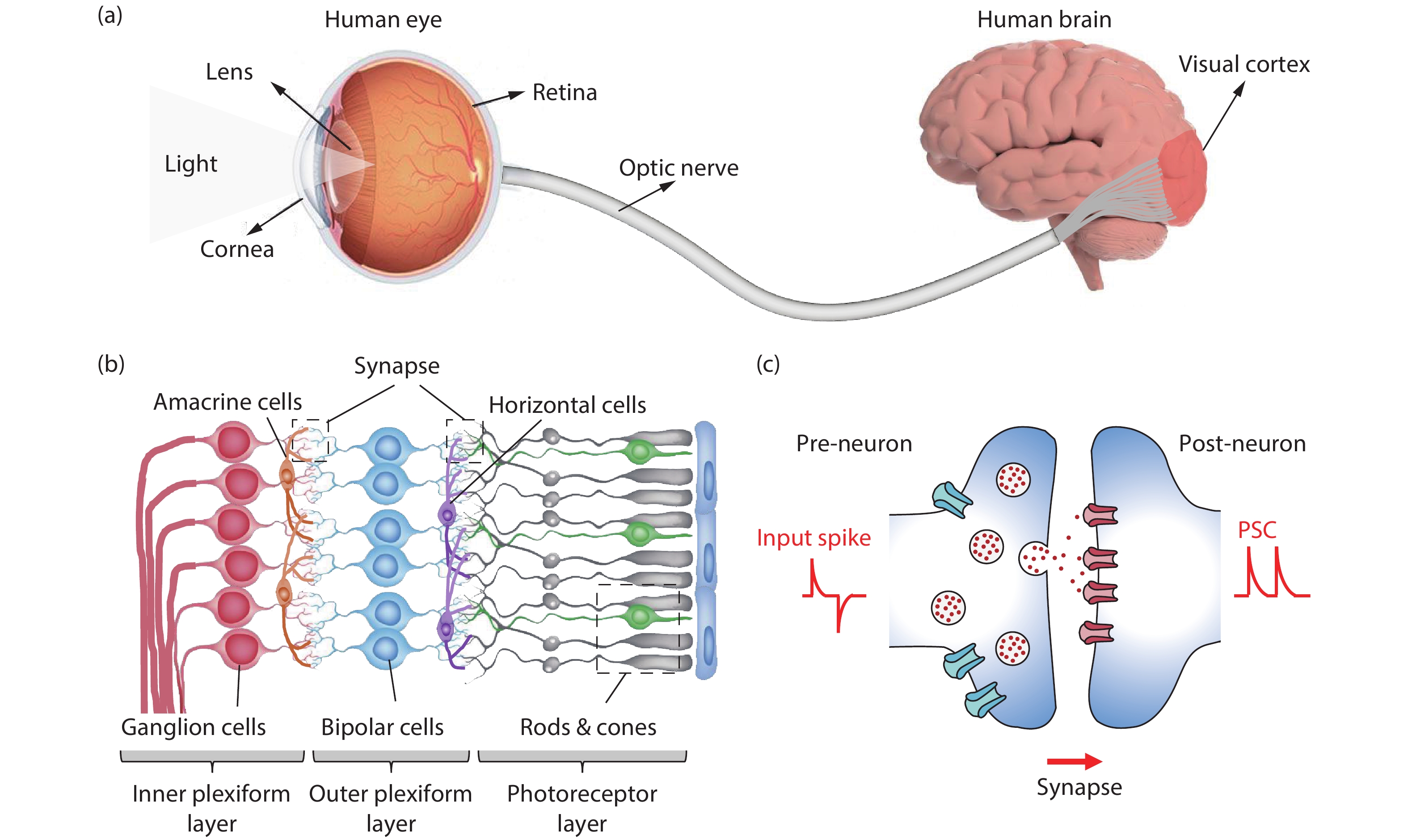
Fig. 1. (Color online) Schematic diagram of (a) the composition of human visual system, (b) multilayer structure of human retina, and (c) a biological synapse.
![(Color online) (a) Abstracted pixel schematic of DVS. (b) Principle of operation[45]. (c) The response of a DVS array to a person moving in the field of view of the sensor. (d) A DVS array is observing a 500 Hz spiral on an analog oscilloscope. (e) The DVS output is a continuous sequence of address events (x, y) in time. Red and blue events represent an increase or decrease change of light, respectively[15].](/richHtml/jos/2021/42/1/013105/img_2.jpg)
Fig. 2. (Color online) (a) Abstracted pixel schematic of DVS. (b) Principle of operation[45 ]. (c) The response of a DVS array to a person moving in the field of view of the sensor. (d) A DVS array is observing a 500 Hz spiral on an analog oscilloscope. (e) The DVS output is a continuous sequence of address events (x , y ) in time. Red and blue events represent an increase or decrease change of light, respectively[15 ].
Fig. 3. (Color online) (a) Abstracted pixel schematic of ATIS pixel. (b) The principle of operation of two types of asynchronous AER events. (c) Change detection events recorded (upper) and gray-level updates at the corresponding pixel positions (below)[15 , 16 ].
Fig. 4. (Color online) The circuit and output of DAVIS vision sensor. (a) The pixel circuit of DAVIS pixel combines an APS with a DVS. (b) A snapshot from DAVIS sensors illustrating a captured APS frame in gray scale with the DVS events in color. The football was flying toward the person. Inset: 5 ms of output right after the frame capture of the football. (c) Space-time 3D view of DVS events during 40 ms of a white rectangle spinning on a black disk at 100 Hz. Green events are older and red events are newer[49 ].
Fig. 5. (Color online) Neuromorphic vision sensors based on ORRAM. (a) I–V characteristics of ORRAM with optical set and electrical reset. Inset, schematic structure of the MoOx ORRAM and its cross-section scanning electron microscopy (SEM) image. Scale bar, 100 nm. (b) Light-tunable synaptic characteristics under light intensity of 0.22, 0.45, 0.65 and 0.88 mW/cm2, respectively, with a pulse width of 200 ms. (c) Illustrations of the image memory function of ORRAM array. The letter F was stimulated with a light intensity of 0.88 mW/cm2. (d) Images before (left columns) and after (right columns) ORRAM image sensor pre-processing. (e) The image recognition rate with and without ORRAM image preprocessing[17 ].
Fig. 6. (Color online) NN vision sensors. (a) Schematic of the 2D Perovskite/Graphene optical synaptic device[21 ]. (b) Schematic of an artificial optic-neural synapse device based on h-BN/WSe2 heterostructure[20 ]. (c) Optical image of WSe2/h-BN/Al2O3 vdW heterostructure based device (left) and its structural diagram (right)[19 ]. (d) Optical microscope image of the photodiode array consisting of 3 × 3 pixels. The upper right: Schematic of a WSe2 photodiode. The bottom right: SEM image of the pixel. (e) Schematics of the classifier. (f) Schematics of the autoencoder[18 ].
Fig. 7. (Color online) A hemispherical retina based on perovskite nanowire array and its properties. (a) Side view of a completed EC-EYE. (b) The structure diagram of the EC-EYE. (c) Photocurrent and responsivity depend on light intensity of a perovskite nanowire photoreceptor. (d) I–V characteristics and the response of individual pixels. (e) The comparison of field of view (FOV) of the planar and hemispherical image sensors. (f) The reconstructed letter ‘A’ image of EC-EYE and its projection on a flat plane[23 ].
|
Table 1. Comparison of three representative silicon retina.
|
Table 2. Comparisons of neuromorphic vision sensors based on emerging devices.


Set citation alerts for the article
Please enter your email address

© Copyright 2018-2021 | Chinese Laser Press. All Rights Reserved 沪ICP备15018463号-20