Abstract
Conventional frame-based image sensors suffer greatly from high energy consumption and latency. Mimicking neurobiological structures and functionalities of the retina provides a promising way to build a neuromorphic vision sensor with highly efficient image processing. In this review article, we will start with a brief introduction to explain the working mechanism and the challenges of conventional frame-based image sensors, and introduce the structure and functions of biological retina. In the main section, we will overview recent developments in neuromorphic vision sensors, including the silicon retina based on conventional Si CMOS digital technologies, and the neuromorphic vision sensors with the implementation of emerging devices. Finally, we will provide a brief outline of the prospects and outlook for the development of this field.1. Introduction
The computational methods of biological nervous system have been applied to artificial information processing units for decades[1, 2]. The “neuromorphic engineering” was first proposed by Carver Mead in the late 1980s, in which electronic systems can mimic neural architecture in biological nervous systems to improve information processing efficiency[3, 4]. Neuromorphic electronic systems are analogue, self-adaptive, error-tolerant and scalable, and they can process information energy-efficiently, asynchronously, event-driven, and quickly. Neuromorphic electronic systems are much more energy efficient, which consume ten thousand times less power than digital systems, and are much more resistant to component degradation and failure than traditional digital systems[5].
Neuromorphic functions can be implemented by conventional digital very large-scale integration (VLSI) based on transistors or emerging devices. The integrated circuits based on complementary metal–oxide–semiconductor (CMOS) field-effect transistor (FET) can realize models of voltage-controlled neurons and synapses[6]. But they face an important challenge in large-scale integrations, because typically more than dozens of transistors are used to realize the function of one synapse or neuron[7]. In recent years, a few types of emerging devices, such as resistive switching memories[8, 9], phase-change memories[10, 11], synaptic transistors[12, 13], and atom switch memories[14], have been proposed to mimic synaptic functions. Artificial synapses with these devices have advantages of small cell size, simple device structure, low operating voltage, and ease of large-scale integration.
In conventional imaging systems, the image sensing and processing units are physically separated, which causes high power consumption because of data movement between sensing and computing units, greatly limiting their applications with increasing demand for low-power and real-time processing. Inspired by the low-power and high-efficient characteristics of human eye, there have been lots of works about emulating the functions of human eye with semiconductor devices and circuits, including silicon retina[15, 16], optoelectronic random-access memory (ORAM) vision sensors[17], neural network (NN) vision sensors[18-21] and hemispherically shaped vision sensors[22, 23].
2. Conventional frame-based image sensors
Current mainstream image sensors are based on semiconductor technology. There are mainly two types, including charge coupled devices (CCD)[24, 25] and CMOS active pixel sensors (APS)[26, 27]. Conventional visual system consists of two-dimensional (2D) image sensors array (CCD or APS) to perceive the external environmental information inputs as digital images, a memory unit to store the captured visual information, and a processing unit to execute computer vision algorithms for image-processing tasks, such as object recognition and object tracking[28-32]. These sensors are driven by artificially created timing and controlled by artificially created digital signals, and acquire the visual information as a series of ‘‘snapshot’’ images (frames). The quantized visual information in time domain at a predetermined frame rate is not related to the dynamics present in the real world. Each recorded frame conveys the information from all pixels, even the information is unchanged since the last frame was acquired[33].
Conventional image sensors face great limitations resulting from the frame-based operation. Low frame rate gives rise to the loss of key information, while a high frame rate inevitably results in too much redundant data. This shortcoming becomes very obvious for data-intensive and delay-sensitive applications, such as high-speed motor control, autonomous robot navigation, etc. These sensors generate a lot of redundant data from the frame-based acquisition of visual information. The large amount of visual information is usually converted to a digital electronic format and pass to a computing unit for image processing. The data movement between sensors and processing unit lead to delays (latency), increased communication bandwidth requirements, and high-power consumption.
3. Biological retina and synapse
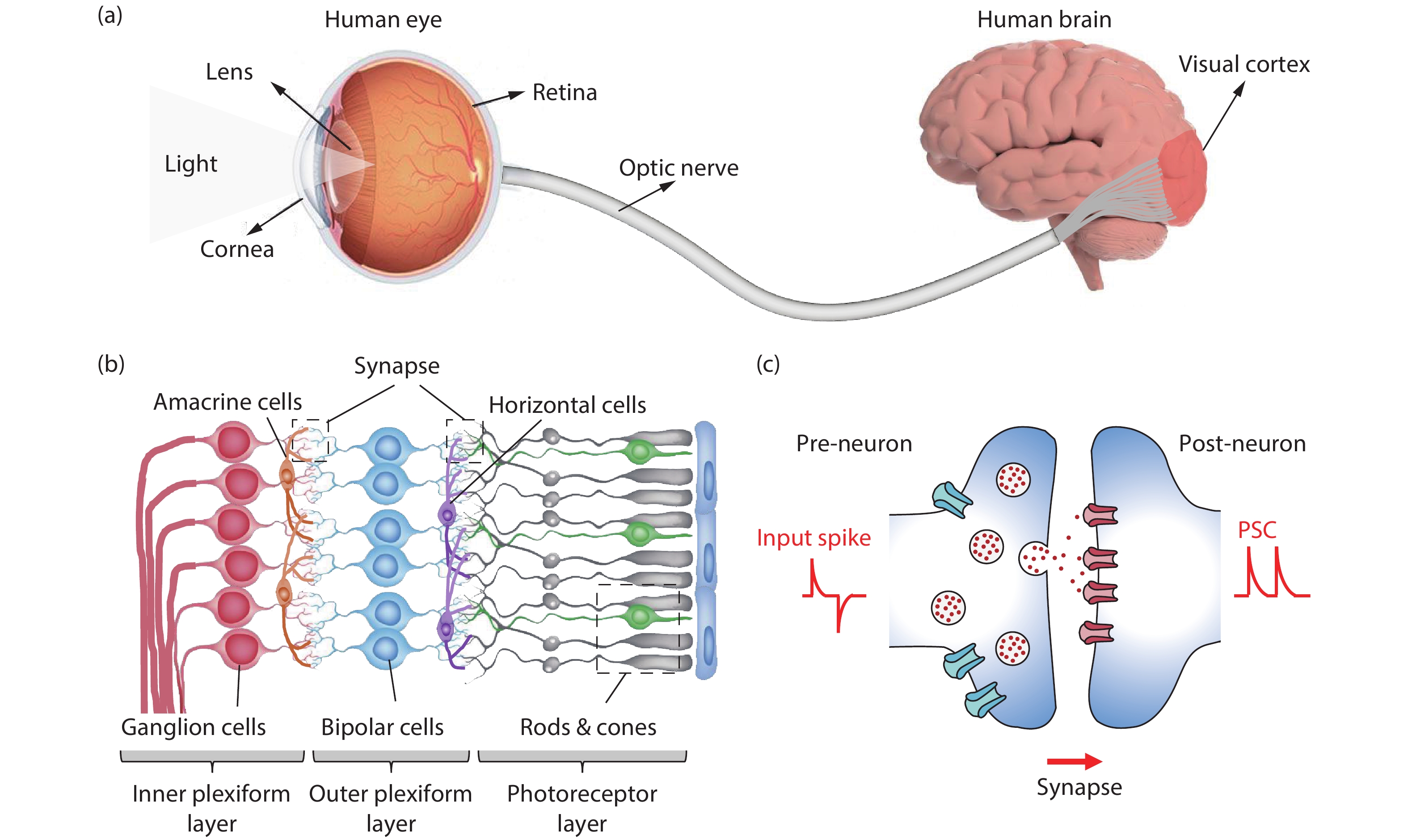
Human visual system mainly consists of eye, optic nerve and brain visual cortex (Fig. 1(a)). The visual information is first passed through the lens, and then perceived and preprocessed by the retina in the human eye, and the extracted information is further passed through optic nerves and finally processed in the visual cortex. A principal function of the human retina is to extract key features of the input visual information by preprocessing operations, which aims to discard the redundant visual data and substantially accelerates further information processing in the human brain, such as pattern recognition and interpretation[34].

Figure 1.(Color online) Schematic diagram of (a) the composition of human visual system, (b) multilayer structure of human retina, and (c) a biological synapse.
As illustrated by Fig. 1(b), the human retina is a complex structure that consist of three primary layers: the photoreceptor layer, the outer plexiform layer, and the inner plexiform layer[15, 35]. More than 50 kinds of different cells are distributed in the human retina, such as the photoreceptors, the bipolar cells, and the ganglion cells. The photoreceptors (e.g., cones for color recognition and sharp vision, rods for vision under dim light conditions[36]) transduce visual signals into electrical potential, while the bipolar cells and ganglion cells serve as the critical harbors for shaping input signals, which can accelerate perception in the brain. The bipolar cells can be divided to the ON cells and the OFF cells. The former code for bright and the latter code for dark spatio–temporal contrast changes. The bipolar and ganglion cells can be further divided into two different groups: the cells with more sustained responses and the cells with more transient responses. There are at least two parallel pathways: the magno-cellular pathway, where cells are sensitive to temporal changes in the scene (biological “where” system), and the parvo-cellular pathway where cells are sensitive to forms in the scene (biological “what” system)[15, 37].
In the (retina) nerve system, the synapse is a specialized structure that allows a neuron to pass chemical or electrical signals to another neuron or to the target effector cell (Fig. 2(c))[38]. The synapse possessed special synaptic plasticity (the change in synaptic weight), which is the fundamental mechanism of memory and learning process in biological nervous system. In general, synaptic plasticity can be divided into two main parts: short-term plasticity (STP) and long-term plasticity (LTP)[39, 40]. STP in the hippocampus is a temporal change in synaptic connection and will rapidly decay to its original state after removing the external spike. In contrast, LTP is a longstanding transform in synaptic connection and it is crucial for memory and learning.
Figure 2.(Color online) (a) Abstracted pixel schematic of DVS. (b) Principle of operation[45]. (c) The response of a DVS array to a person moving in the field of view of the sensor. (d) A DVS array is observing a 500 Hz spiral on an analog oscilloscope. (e) The DVS output is a continuous sequence of address events (x, y) in time. Red and blue events represent an increase or decrease change of light, respectively[15].
The human retina has a hierarchical biostructure for connectivity among neurons with distinct functionalities and enables simultaneous sensing and preprocessing of visual information. Emulating the structures and functionalities of the human retina provide a promising and effective way to achieve vision sensor with low-power and high-efficient image processing.
4. Conventional neuromorphic vision sensor
In conventional neuromorphic vision devices, also name as silicon retina, various vision sensors based on integrated circuits have been developed over the past two decades, including temporal contrast vision sensors, gradient-based sensors, edge-orientation sensitive sensors, and optical flow sensors[41-43]. However, very few have been used in practical applications, because of circuit complexity, low integration level, and high noise level[33]. More recently, there have been many improvements in vision sensors based on biological principles in terms of performance and practicality. These sensors include dynamic vison sensors (DVS)[44-46], asynchronous time-based image sensors (ATIS)[47, 48], and recently developed dynamic and active pixel vision sensors (DAVIS)[49, 50]. There have a few excellent reviews on conventional neuromorphic vision sensors[15, 16, 33, 37]. In this section, we will show a brief introduction of their research progress.
4.1. DVS
To implement a practicable vision sensor based on the functions of the magno-cellular transient pathway in retina, researchers proposed the DVS[44-46, 51]. The DVS emulates a simplified three-layer retina (Fig. 2(a)) to realize an abstraction of information flow through the photoreceptor, bipolar, and ganglion cells. The photo-current is logarithmically encoded by the photoreceptor circuit and output voltage Vp. The differentiation circuit amplifies the changes with high precision and output Vdiff. The comparators compare the Vdiff against global thresholds that are offset from the reset voltage to detect increasing and decreasing changes. If Vdiff is larger than the threshold, an ON or OFF event is generated. Fig. 2(b) shows the mechanism of operation of each pixel. Fig. 2(c) illustrates the response of a DVS pixel array to a natural scene. Events are collected over tens of milliseconds, and displayed as an event map image with ON (going brighter) and OFF (going darker) events, as depicted by white and black dots. Figs. 2(d) and 2(e) illustrate an example of an array of DVS observing a light dot on an analog oscilloscope screen moving in a spiral pattern, which is repeated at a frequency of 500 Hz, exhibiting the fast, high-temporal-resolution operation of event response[15].
The DVS is sensitive to the scene dynamics and directly responds to changes, i.e., temporal contrast with individual pixel. Compared with frame-based image sensors, the gain of DVS is dramatic in terms of temporal resolution. Other parameters, e.g., the intra-scene dynamic range, also greatly benefit from the bio-inspired approach. The DVS is suitable for the machine vision applications, involving high-speed motion detection and analysis, object tracking, and shape recognition.
4.2. ATIS
Posch and co-workers developed the ATIS[47, 48], which incorporates the “where” and “what” system. As shown in Fig. 3(a), this ATIS sensor consists of an event-based change detector (CD) that detects changes in the event stream and an exposure measurement (EM) unit based on pulse width modulation (PWM) that gains event-based intensity values. An EM is executed when it is triggered by a change detection. As a result, two types of asynchronous address-event representation (AER) events, encoding change and exposure information, are generated and transmitted separately (Fig. 3(b)). From a biological retina point of view, the CD unit (similar to DVS pixel) works as a magno-cellular structure (“where” system), while the additional EM unit represents biological parvo-cellular structure (“what” system). Fig. 3(c) display an example of change detection events recorded during a short time window and associated gray-level updates at the corresponding pixel positions.
Figure 3.(Color online) (a) Abstracted pixel schematic of ATIS pixel. (b) The principle of operation of two types of asynchronous AER events. (c) Change detection events recorded (upper) and gray-level updates at the corresponding pixel positions (below)[15, 16].
For the first time, the development of ATIS showed the possibility to obtain static and dynamic image information in parallel. The duality opens up a large number of new processing capabilities, because many conventional machine vision algorithms do not work with asynchronous event streams. The special design and operating principle of the ATIS also offers further advantages and makes it close to practical applications. For example, video compression at sensor level can be achieved by suppressing temporal redundancies. In addition, the extremely high temporal resolution (50–100 kfps equivalent) and the dynamic range of 143 dB are remarkable.
4.3. DAVIS
DAVIS is another approach to combine dynamic and static information into a single pixel[49, 50], which combines both DVS and APS. As presented in Fig. 4(a), the DVS circuit is responsible for the asynchronous detection of logarithmic intensity changes, generating dynamic scene information. The second component of the DAVIS is an APS, similar to the EM of ATIS, which is responsible for absolute exposure measurement and generates gray-scale images in addition to the event stream. Different from ATIS, the additional component of DAVIS is not asynchronous. The APS circuit receives static scene information by frame-based sampling of the intensities. Fig. 4(b) illustrates the combined output of both DVS and APS readouts when a person is catching a football. The output illustrates the sparseness of the DVS output (colored), in which the events are mainly produced by the moving ball while most pixels stay silent. Inset of Fig. 4(b) demonstrates the temporal accuracy and resolution of the DVS events. A 5 ms slice of DVS events (colored) acquired 75 ms after the APS frame highlights the contours of the ball. Fig. 4(c) shows a space-time view of the DVS data generated by a 100 Hz spinning rectangle. Because of the asynchronous nature of the DVS output, the sensor can capture high-speed motion exceeding 40 000 pixels/s.
Figure 4.(Color online) The circuit and output of DAVIS vision sensor. (a) The pixel circuit of DAVIS pixel combines an APS with a DVS. (b) A snapshot from DAVIS sensors illustrating a captured APS frame in gray scale with the DVS events in color. The football was flying toward the person. Inset: 5 ms of output right after the frame capture of the football. (c) Space-time 3D view of DVS events during 40 ms of a white rectangle spinning on a black disk at 100 Hz. Green events are older and red events are newer[49].
The DAVIS has the advantages over the DVS circuit. For example, the APS shares same one photodiode with the DVS component. The simple readout circuit of DAVIS only has a few transistors, increasing the DVS pixel area by approximately 5%. It allows to capture framed images, but collects redundant data.
4.4. Summary of a conventional neuromorphic vision sensor
In this part, we compare three representative neuromorphic vision sensors based on conventional Si CMOS technology. Table 1 documents the specifications of the reported DVS, ATIS, and DAVIS. The DVS is a bioinspired “where” system that responds to relative illumination changes. The ATIS is a combination of bioinspired “where” and “what” systems that contains event-based CD and PWM-based EM units. Both the DVS and the ATIS are based on an asynchronous event-driven method, and the single pixel can handle its own visual information individually and autonomously. The DAVIS is a combination of an asynchronous “where” system and a synchronous “what” system. It outputs image frames by the synchronous APS pathway and simultaneously outputs events by the asynchronous DVS pathway.
Table Infomation Is Not Enable
The common shortcomings of these technologies are very complex circuit, a large pixel area and a low filling factor. Conventional neuromorphic vision sensors have been applied to various computer vision and robotics applications, but still face the challenges in terms of low-integration level, high-power consumption and latency.
5. Emerging neuromorphic vision sensors
The neuromorphic vision sensors implemented by silicon retina based on CMOS technology suffer from the shortcomings of circuit complexity, large pixel area, low fill factors, and high noise level. In contrast to the complex structure of silicon retina, the neuromorphic vision sensors based on emerging devices is simple and compact, which potentially decreases power consumption and increases response speed. For example, ORAM devices offer great opportunities for multifunctional integration of optical sensing, data storage and pre-processing functions into one single device[52]. Recently, researchers reported emerging neuromorphic vision sensors, include ORAM vision sensors[17], NN vision sensors[18-21] and hemispherically shaped vision sensors[22, 23].
5.1. ORAM vision sensors
Compare to traditional random-access memories (RAMs) that are usually manipulated by electrical triggers, ORAM has alternative way modulated by optical excitation, which enables the ORAM to integrate the functions of both optical sensing and preprocessing, and can realize the part of the functions of artificial retina. The ORAM shows great potential for bridging the gap between optical sensing and neuromorphic computing which results in simplifying the neuromorphic vision sensor circuitry and reducing the power consumption. The current ORAMs are mainly divided into two types: three-terminal FET memory[53-60] and two-terminal optoelectronic resistive random-access memories (ORRAMs)[17, 52, 61-63].
Researchers have demonstrated excellent works about ORAM vision sensors[17, 53, 58, 64]. For example, Zhou et al.[17] demonstrated an ORRAM synaptic device with two-terminal of Pd/MoOx/ITO (indium tin oxide) that shows ultraviolet (UV) light sensing, optically triggered non-volatile and volatile resistance switching and light-tunable synaptic behaviors (Figs. 5(a) and 5(b)). The ORRAM arrays allow us to achieve the functions of image sensing and memorization, as well as preprocessing (Fig. 5(c)). The image preprocessing functions are implemented based on the light-dosage tunable plasticity of the ORRAM device. The input and output images after the preprocessing are compared in Fig. 5(d). After the preprocessing through ORRAM arrays, the body features of the letters were highlighted and the background noise signals were smoothed. The image preprocessing can further improve the efficiencies in image recognition process. Fig. 5(e) shows the recognition rate of visual systems with and without ORRAM, and illustrates obvious improvements in the recognition rate and efficiency with the use of ORRAMs for the image preprocessing.
Figure 5.(Color online) Neuromorphic vision sensors based on ORRAM. (a) I–V characteristics of ORRAM with optical set and electrical reset. Inset, schematic structure of the MoOx ORRAM and its cross-section scanning electron microscopy (SEM) image. Scale bar, 100 nm. (b) Light-tunable synaptic characteristics under light intensity of 0.22, 0.45, 0.65 and 0.88 mW/cm2, respectively, with a pulse width of 200 ms. (c) Illustrations of the image memory function of ORRAM array. The letter F was stimulated with a light intensity of 0.88 mW/cm2. (d) Images before (left columns) and after (right columns) ORRAM image sensor pre-processing. (e) The image recognition rate with and without ORRAM image preprocessing[17].
5.2. NN vision sensors
For conventional image processing with neuromorphic computing, the optical signals in the images are first converted to electronic signals through image sensors. The electronic signals are then transferred to the neural network for further complicated processing. The movement of redundant data between sensor and processing unit leads to delays and high-power consumption in conventional vision system[65]. To solve these problems, researchers demonstrated NN vision sensors with in-sensor computing ability for highly efficient processing. Tian et al.[21] reported an artificial optical synapse array based on a graphene/2D perovskite heterostructure for pattern recognition, showing a high accuracy rate of 80% (Fig. 6(a)). Seo et al.[20] further demonstrated an optic-neural network (ONN) based on WSe2/h-BN heterostructure for emulating the function of color-mixed pattern recognition in human vision (Fig. 6(b)). The recognition rate for mixed-color digits in ONN is about 60% higher than that of NN.
Figure 6.(Color online) NN vision sensors. (a) Schematic of the 2D Perovskite/Graphene optical synaptic device[21]. (b) Schematic of an artificial optic-neural synapse device based on h-BN/WSe2 heterostructure[20]. (c) Optical image of WSe2/h-BN/Al2O3 vdW heterostructure based device (left) and its structural diagram (right)[19]. (d) Optical microscope image of the photodiode array consisting of 3 × 3 pixels. The upper right: Schematic of a WSe2 photodiode. The bottom right: SEM image of the pixel. (e) Schematics of the classifier. (f) Schematics of the autoencoder[18].
More recently, Wang et al.[19] designed an image sensor based on the WSe2/h-BN/Al2O3 van der Waals (vdW) heterostructures (Fig. 6(c)). The NN based on such devices can achieve reconfigurable vision sensor for simultaneously image sensing and processing. In addition, a convolutional NN formed by the sensors can be trained to classify the input images. Mennel and co-workers[18] implemented an artificial neural network (ANN) in their image sensor that simultaneously senses and process optical images near real-time. The NN image sensor consists of N pixels and M subpixels (Fig. 6(d)). Each subpixel is based on a WSe2 photodiode with tunable photo-responsivity by split-gate voltage. They demonstrated both supervised (e.g., a classifier (Fig. 6(e))) and unsupervised learning (e.g., an autoencoder (Fig. 6(f)) algorithms using the NN vision sensor. The classification and autoencoding can be implemented at a throughput of 20 million bits per second with optically projected onto the chip. The NN vision sensor device has great potential to large-scale integration and provides various algorithms for ultrafast machine vision applications.
5.3. Hemispherically shaped vision sensors
A hemispherical vision sensor design with broad view angle is important for humanoid robots. However, commercial CCD, APS image sensors and silicon retina are mainly dependent on planner device structures by conventional planar microfabrication processes, which is difficult to fabricate hemispherical devices. Previously, there have been some reported works about hemispherical image sensors by utilize curved, folded, or individually assembled photodetectors[22, 30, 32, 66]. These photodetectors were mainly pre-fabricated on planar substrates, then transferred to a hemispherical supporting material or folded into a hemispherical shape. This design limits the density of the imager pixels, because space had to be reserved between them to allow for the transfer or folding.
More recently, Gu et al.[23] demonstrated an artificial visual system using a spherical biomimetic electrochemical eye (EC-EYE) with a hemispherical retina. They constructed the artificial retina with a high-density perovskite nanowire (Figs. 7(a) and 7(b)). An ionic liquid electrolyte was used as a front-side common contact to the nanowires, and liquid-metal wires (eutectic gallium indium in soft rubber tubes) were used as back contacts to the nanowire photosensors, mimicking human nerve fibers behind the retina. Device characterizations show that the EC-EYE has a high responsivity (303.2 mA/W) (Fig. 6(c)), a reasonable response speed (response time 19.2 ms, recovery time 23.9 ms) (Fig. 6(d)), a low detection limit (0.3 μW/cm2) and a wide field of view (100°) (Fig. 6(e)). In addition to its structural similarity with a human eye, the hemispherical artificial retina has a nanowire density much higher than that of photoreceptors in a human retina and can thus potentially achieve higher image resolution (4.6 × 108 cm–2). The authors also demonstrated the image-sensing functions of the biomimetic device by reconstructing the optical patterns projected onto the device (Fig. 7(f)). This work may lead to biomimetic photosensing devices that can be used in a wide spectrum of technological applications.
Figure 7.(Color online) A hemispherical retina based on perovskite nanowire array and its properties. (a) Side view of a completed EC-EYE. (b) The structure diagram of the EC-EYE. (c) Photocurrent and responsivity depend on light intensity of a perovskite nanowire photoreceptor. (d) I–V characteristics and the response of individual pixels. (e) The comparison of field of view (FOV) of the planar and hemispherical image sensors. (f) The reconstructed letter ‘A’ image of EC-EYE and its projection on a flat plane[23].
5.4. Summary of emerging neuromorphic vision sensor
In this section, we summarize the state-of-the-art progress and performance of neuromorphic vision sensors based on various emerging devices. Table 2 compares various emerging devices based neuromorphic vision sensors. ORAM synaptic devices allow for achieving the functions of image sensing and preprocessing, as well as memory, showing promise in reducing the complex circuitry for an artificial visual system. However, the ORAM requires the operation process of optically SET and electrically RESET, which limits its further application in neuromorphic network. Furthermore, it still requires to further reduce the energy consumption, comparable to per synaptic operation in a biological neural network (10–15 J)[67].
Table Infomation Is Not Enable
NN image sensors based on various semiconductor materials, especially 2D materials can simultaneously perceive and process optical images information near real-time, which show great potential for ultrafast machine vision applications[64]. However, this type of neuromorphic visual system for self-driving automobile and robotics will need to capture stereo dynamic images with a wide field of view. Its planar shape will limit its further application[22].
Hemispherically shaped image sensors have high similarity with human eye structure, which is expected to achieve high imaging resolution and a wide FOV. Such a biomimetic eye has great potential applications in humanoid robots and human eye prosthesis. However, the pixels in the hemispherically shaped image sensors consist of photodetectors without the functions of information memory and preprocessing. The light information converts to electric signals and then transfer to an external information processing unit, like conventional digital visual system. Moreover, the fabrication process involves some costly and low-throughput steps.
6. Perspectives
Leveraged on matured Si CMOS technologies, most of existing works about neuromorphic vision sensors are based on the Si integrated circuits, such as silicon retina. Silicon retinas have been developed for decades, and were demonstrated with several representative prototypes, such as DVS, ATIS, and DVAIS. However, they have faced an obvious shortcoming of high-density integrations due to its circuit complexity, large pixel area, low fill factors and poor uniformity of pixel response characteristics[45]. Silicon retina are mainly fabricated by mainstream planar microfabrication processes, which makes it difficult to construct hemispherical shape, greatly restricts the applications of wide-field camera, and leads to the optical aberration. In addition, their intrinsically digital characteristics results in the inefficiency of implementing neuromorphic algorithms.
By exploiting emerging devices with analogue characteristics and new working principle, it can offer alternative approaches to realize neuromorphic vision sensors with high energy efficiency and high response speed. Although intense progress has been obtained in emerging devices for neuromorphic vision sensor applications, there are still some grand challenges. For example, during the learning and forgetting process, light stimuli is mainly used to achieve potentiation behavior, whereas electric stimuli is utilized for the depression behavior. Hence, it also requires to obtain the habituation characteristics under light stimulus. Thus, it is important to emulate sophisticated neural functionalities through the optical modulation. In addition, the 2D shape of existing vision sensor arrays also hinder the development of wide-field cameras. For hemispherically shaped image sensors, the complexity and cost of the fabrication process are obvious problems. In the future, how to make full use of optoelectronic devices to form a large-scale hemispherical shaped NN image sensor is an important research direction, which is expected to realize a low-power consumption, real-time, and highly bionic machine vision system.
Acknowledgements
This work is supported by Research Grant Council of Hong Kong (15205619), the Shenzhen Science and Technology Innovation Commission (JCYJ20180507183424383), and National Natural Science Foundation of China (61851402).
References
[1] A logical calculus of the ideas immanent in nervous activity. Bull Math Biophys, 5, 115(1943).
[2]
[3]
[4] et alImplementing neural architectures using analog VLSI circuits. IEEE Trans Circuits Syst, 36, 643(1989).
[5] Neuromorphic electronic systems. Proc IEEE, 78, 1629(1990).
[6] A quantitative description of membrane current and its application to conduction and excitation in nerve. J Physiol, 117, 500(1952).
[7] et alA million spiking-neuron integrated circuit with a scalable communication network and interface. Science, 345, 668(2014).
[8] The future of electronics based on memristive systems. Nat Electron, 1, 22(2018).
[9] et al2D layered materials for memristive and neuromorphic applications. Adv Electron Mater, 6, 1901107(2019).
[10] et alStochastic phase-change neurons. Nat Nanotechnol, 11, 693(2016).
[11] et alNanoelectronic programmable synapses based on phase change materials for brain-inspired computing. Nano Lett, 12, 2179(2012).
[12] et alA synaptic transistor based on quasi-2D molybdenum oxide. Adv Mater, 29, 1700906(2017).
[13] et alAnisotropic black phosphorus synaptic device for neuromorphic applications. Adv Mater, 28, 4991(2016).
[14] et alShort-term plasticity and long-term potentiation mimicked in single inorganic synapses. Nat Mater, 10, 591(2011).
[15] et alRetinomorphic event-based vision sensors: bioinspired cameras with spiking output. Proc IEEE, 102, 1470(2014).
[16] et alNeuromorphic stereo vision: A survey of bio-inspired sensors and algorithms. Front Neurorobot, 13, 28(2019).
[17] et alOptoelectronic resistive random access memory for neuromorphic vision sensors. Nat Nanotechnol, 14, 776(2019).
[18] et alUltrafast machine vision with 2D material neural network image sensors. Nature, 579, 62(2020).
[19] et alGate-tunable van der Waals heterostructure for reconfigurable neural network vision sensor. Sci Adv, 6, eaba6173(2020).
[20] et alArtificial optic-neural synapse for colored and color-mixed pattern recognition. Nat Commun, 9, 1(2018).
[21]
[22] et alHuman eye-inspired soft optoelectronic device using high-density MoS2-graphene curved image sensor array. Nat Commun, 8, 1(2017).
[23] et alA biomimetic eye with a hemispherical perovskite nanowire array retina. Nature, 581, 278(2020).
[24] Charge coupled semiconductor devices. Bell Syst Tech J, 49, 587(1970).
[25]
[26]
[27] et alReview of CMOS image sensors. Microelectron J, 37, 433(2006).
[28] et alA bioinspired flexible organic artificial afferent nerve. Science, 360, 998(2018).
[29] et alBioinspired artificial eyes: Optic components, digital cameras, and visual prostheses. Adv Funct Mater, 28, 1705202(2017).
[30] et alDigital cameras with designs inspired by the arthropod eye. Nature, 497, 95(2013).
[31] Biologically inspired artificial compound eyes. Science, 312, 557(2006).
[32] et alA hemispherical electronic eye camera based on compressible silicon optoelectronics. Nature, 454, 748(2008).
[33] Bio-inspired vision. J Instru, 7, C01054(2012).
[34] Eye smarter than scientists believed: Neural computations in circuits of the retina. Neuron, 65, 150(2010).
[35] The fundamental plan of the retina. Nat Neurosci, 4, 877(2001).
[36]
[37] A review of bioinspired vision sensors and their applications. Sens Mater, 27, 447(2015).
[38] Electrical synapses and their functional interactions with chemical synapses. Nat Rev Neurosci, 15, 250(2014).
[39] et alSynaptic metaplasticity realized in oxide memristive devices. Adv Mater, 28, 377(2016).
[40] et alMixed-halide perovskite for ultrasensitive two-terminal artificial synaptic devices. Mater Chem Front, 3, 941(2019).
[41] Neuromorphic vision sensors. Sens Actuators A, 56, 19(1996).
[42] Neuromorphic vision sensors. Science, 288, 1189(2000).
[43]
[44]
[45] A 128 × 128 120 dB 15 μs latency asynchronous temporal contrast vision sensor. IEEE J Solid-State Circuits, 43, 566(2008).
[46] A 3.6 μs latency asynchronous frame-free event-driven dynamic-vision-sensor. IEEE J Solid-State Circuits, 46, 1443(2011).
[47] A QVGA 143 dB dynamic range frame-free pwm image sensor with lossless pixel-level video compression and time-domain CDS. IEEE J Solid-State Circuits, 46, 259(2011).
[48]
[49]
[50] et alA 240 × 180 130 dB 3 μs latency global shutter spatiotemporal vision sensor. IEEE J Solid-State Circuits, 49, 2333(2014).
[51] A 64 × 64 AER logarithmic temporal derivative silicon retina. Research in Microelectronics and Electronics, 2005 PhD, 2, 202(2005).
[52] et alLow-voltage, optoelectronic CH3NH3PbI3–xClx memory with integrated sensing and logic operations. Adv Funct Mater, 28, 1800080(2018).
[53] et alOptoelectronic memory using two-dimensional materials. Nano Lett, 15, 259(2015).
[54] et alMonolayer optical memory cells based on artificial trap-mediated charge storage and release. Nat Commu, 8, 14734(2017).
[55] et alMultibit MoS2 photoelectronic memory with ultrahigh sensitivity. Adv Mater, 28, 9196(2016).
[56] et alOptoelectrical molybdenum disulfide (MoS2)-ferroelectric memories. ACS Nano, 9, 8089(2015).
[57] et alGraphene–MoS2 hybrid structures for multifunctional photoresponsive memory devices. Nat Nanotechnol, 8, 826(2013).
[58] et alTwo-dimensional multibit optoelectronic memory with broadband spectrum distinction. Nat Commun, 9, 2966(2018).
[59] et alA light-stimulated synaptic device based on graphene hybrid phototransistor. 2D Mater, 4, 035022(2017).
[60]
[61] et alMoS2 memristor with photoresistive switching. Sci Rep, 6, 31224(2016).
[62] et alTwo-terminal multibit optical memory via van der Waals heterostructure. Adv Mater, 31, 1807075(2019).
[63] et alPhosphorene/ZnO nano-heterojunctions for broadband photonic nonvolatile memory applications. Adv Mater, 30, 1801232(2018).
[64] et al2D materials based optoelectronic memory: Convergence of electronic memory and optical sensor. Research, 2019, 9490413(2019).
[65] In-sensor computing for machine vision. Nature, 579, 32(2020).
[66] et alOrigami silicon optoelectronics for hemispherical electronic eye systems. Nat Commun, 8, 1782(2017).
[67] The metabolic cost of neural information. Nat Neurosci, 1, 36(1998).