• Journal of Semiconductors
  • Vol. 40, Issue 6, 062004 (2019)
Pengxiang Bai, Shiying Guo, Shengli Zhang, Hengze Qu, Wenhan Zhou, and Haibo Zeng
Author Affiliations
  • MIIT Key Laboratory of Advanced Display Materials and Devices, School of Materials Science and Engineering, Nanjing University of Science and Technology, Nanjing 210094, China
  • show less
    DOI: 10.1088/1674-4926/40/6/062004 Cite this Article
    Pengxiang Bai, Shiying Guo, Shengli Zhang, Hengze Qu, Wenhan Zhou, Haibo Zeng. Electronic band structures and optical properties of atomically thin AuSe: first-principle calculations[J]. Journal of Semiconductors, 2019, 40(6): 062004 Copy Citation Text show less
    (Color online) Structure of (a) bulk AuSe with 2 × 2 × 1 supercell, (b) two dimensional AuSe in top view and (c) side view. (d) Cleavage energy of AuSe monolayer and black phorphous.
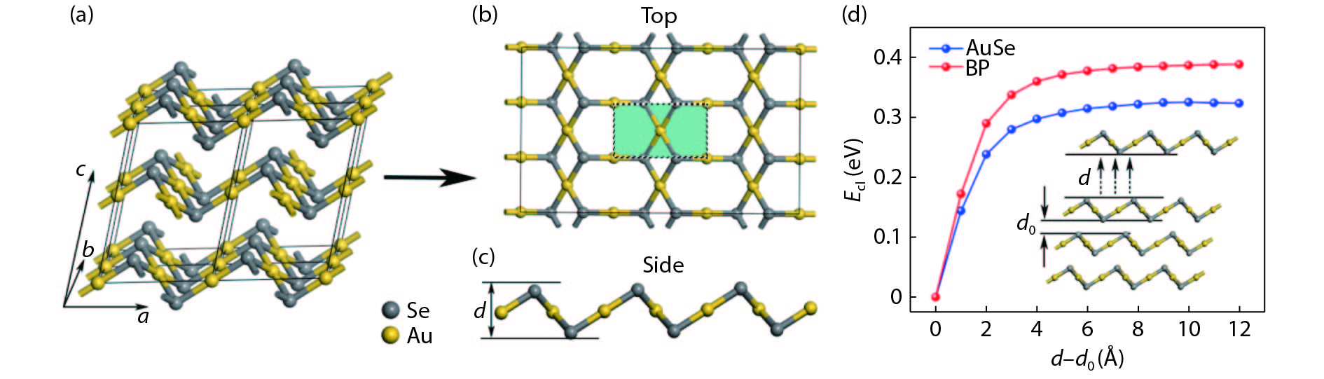
    Fig. 1. (Color online) Structure of (a) bulk AuSe with 2 × 2 × 1 supercell, (b) two dimensional AuSe in top view and (c) side view. (d) Cleavage energy of AuSe monolayer and black phorphous.
    (Color online) (a) Phonon spectrum of AuSe monolayer. (b) Simulation spectrum of Raman shift with exciting wavelength of 514.5 nm at 300 K and corresponding schematic diagram of vibration modes (inset).
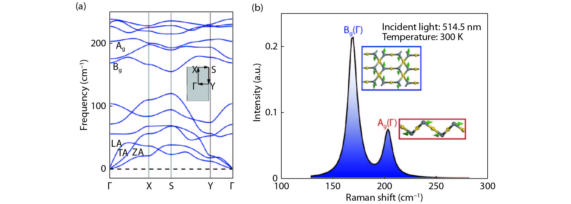
    Fig. 2. (Color online) (a) Phonon spectrum of AuSe monolayer. (b) Simulation spectrum of Raman shift with exciting wavelength of 514.5 nm at 300 K and corresponding schematic diagram of vibration modes (inset).
    (Color online) Electron localization function (ELF) maps of AuSe monolayer, where blue and red regions denote accumulation and depletion of electrons, respectively.
    Fig. 3. (Color online) Electron localization function (ELF) maps of AuSe monolayer, where blue and red regions denote accumulation and depletion of electrons, respectively.
    (Color online) (a) Computed band structure and density of states (DOS) of AuSe monolayer at HSE06, PBE and PBE+SOC levels, charge density of (b) VBM and (c) CBM, isosurface level is 0.0052 e/bohr3.
    Fig. 4. (Color online) (a) Computed band structure and density of states (DOS) of AuSe monolayer at HSE06, PBE and PBE+SOC levels, charge density of (b) VBM and (c) CBM, isosurface level is 0.0052 e/bohr3.
    (Color online) Absorption spectrum of AuSe monolayer with incident light perpendicular to the 2D plane (z direction) and along different directions in the plane (x and y directions).
    Fig. 5. (Color online) Absorption spectrum of AuSe monolayer with incident light perpendicular to the 2D plane (z direction) and along different directions in the plane (x and y directions).
    MaterialBond length (Å)Bond angle (deg)Lattice parameters (deg)
    d1d2θ1θ2θ3αγ
    AuSe2.492.4194.7385.2797.4590.0084.13
    Table 1. Optimized lattice parameters of AuSe monolayer.
    Pengxiang Bai, Shiying Guo, Shengli Zhang, Hengze Qu, Wenhan Zhou, Haibo Zeng. Electronic band structures and optical properties of atomically thin AuSe: first-principle calculations[J]. Journal of Semiconductors, 2019, 40(6): 062004
    Download Citation