
Pengxiang Bai, Shiying Guo, Shengli Zhang, Hengze Qu, Wenhan Zhou, Haibo Zeng. Electronic band structures and optical properties of atomically thin AuSe: first-principle calculations[J]. Journal of Semiconductors, 2019, 40(6): 062004
- Journal of Semiconductors
- Vol. 40, Issue 6, 062004 (2019)
Abstract
1. Introduction
Tracing back to the process of human exploring two-dimension (2D) material, there is no doubt that the discovery of graphene is the originator[
Over past several years, precious metal related TMDs also came into the view of researches and some attractive properties were founded among them. For instance, on the one hand, PtS2 and PtSe2 have strongly bound excitons and rather high mobility[
In this article, all theoretical studies on AuSe monolayer were performed within first-principle calculations. Optimized structure is composed by tri-coordinated Se atoms, tetra- and two-coordinated Au atoms, Se atoms of which grant it zigzag appearance. Double stability (dynamic and thermodynamic stability) was demonstrated by phonon dispersion and cohesive energy calculations. Our calculation results of electronic structure and optical properties revealed that AuSe monolayer is a semiconductor with an indirect band-gap of 2.0 eV, and sensitively responds to deep-UV light. All of computation and discussion done in this reported are significative to better exhibit this precious metal related transition metal selenide.
2. Computational methods
All first-principle calculations were performed on the bias of density functional theory (DFT) as implement in CASTEP code[
3. Result and discussion
3.1. Geometric optimized structure of AuSe monolayer
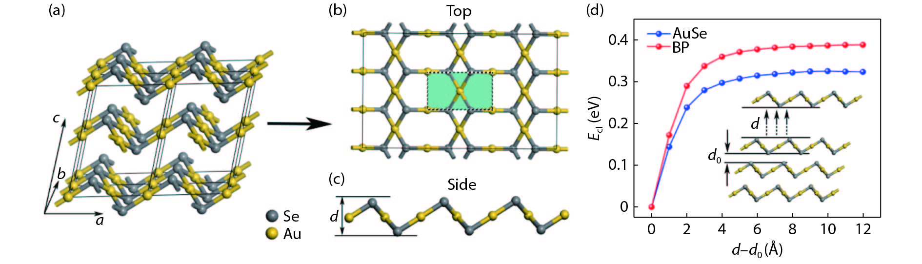
All geometric structural models of bulk and monolayer AuSe are shown in Fig. 1. One could see a clear layered structure in bulk AuSe, indicating 2D AuSe could be easily fabricated by overcoming its weak Van der Waals' coupling between layers. Atomically thin AuSe exhibits unique hexagon-rhombus combined configuration from the top view, and similar buckled structure with group-V 2D materials (phosphorene, arsenene and antimonene) from the side view[
![]()
Figure 1.(Color online) Structure of (a) bulk AuSe with 2 × 2 × 1 supercell, (b) two dimensional AuSe in top view and (c) side view. (d) Cleavage energy of AuSe monolayer and black phorphous.
Table Infomation Is Not Enable3.2. Stability and Raman scattering
Stability is crucial to applying 2D materials to electronic devices. Dynamic stability of crystals can be directly confirmed by calculating the dispersion of phonon band. Hence, the phonon spectrum is simulated and presented in Fig. 2(a) for studying the dynamical stability of AuSe monolayer. All frequencies of lattice vibration are positive, namely, no imaginary modes occur in the entire Brillouin path, indicating AuSe monolayer possesses superior kinetic stability. Cohesive energy is another factor for stability which is often used to judge robust bonding. The specific value is defined as:
![]()
Figure 2.(Color online) (a) Phonon spectrum of AuSe monolayer. (b) Simulation spectrum of Raman shift with exciting wavelength of 514.5 nm at 300 K and corresponding schematic diagram of vibration modes (inset).
where EAu, ESe and EAuSe represent the energy of single gold atom, single selenium atom and AuSe monolayer, respectively, and n denotes the numbers of gold or selenium atoms in AuSe monolayer. The computation result is up to –7.87 eV/atom, which is comparable to that of graphene and h-BN [
In order to reveal information about molecules vibration and rotation in AuSe monolayer, we simulated the Raman scattering spectrum. As shown in Fig. 2(b), there are two remarkable Raman peaks appearing at 168.8 and 203.3 nm, which stem from vibration modes of Bg and Ag, respectively. The intensity of the Bg peak is much stronger than that of Ag, indicating the Bg mode predominates over the Ag mode. In addition, both two modes are corresponding to the frequency of phonons at the centre of Brillouin zone (Gamma point), which could be traced from phonon spectrum. More visualized sketches of vibration modes are inserted in the spectrum beside corresponding peaks, showing that both of them vibrate within the layered plane while no vibration modes is perpendicular to the plane.
3.3. Chemical bonding
Two different coordination forms of gold atoms in AuSe monolayer attract our interest to reveal the types of chemical bonding in this ultrathin crystal. Electron localization function (ELF) is usually computed to obtain the localization of electrons around atoms or along chemical bonds and further to judge the types of chemical bonding[
![]()
Figure 3.(Color online) Electron localization function (ELF) maps of AuSe monolayer, where blue and red regions denote accumulation and depletion of electrons, respectively.
3.4. Electronic structure
The electronic properties are vital for applying new 2D materials to atomically thin nano-electronic components and transistors. The band structure calculated by using HSE06 and GGA-PBE functional are shown in Fig. 4(a), together with density of states (PBE) near fermi level. The bandstructure calculated at all functional levels indicates AuSe monolayer is an indirect band gap semiconductor. The band gap calculated at PBE level is widely known underestimated in recent years, therefore a more precise result of 2.0 eV is obtained by HSE06 functional. Spin orbit coupling (SOC) has been reported to strongly affect bandsturcture of heavier elements related compounds, basing bandstructure inversion mechanism in topological insulators, which is crucial to explain the occurrence of edge states. For more complete characteristic revelation of this emerging material, bandstructure with SOC effect is also calculated at PBE level. However, the result in Fig. 4(a) shows no evident difference after considering SOC effects, only presenting some gap shrink. Hence, AuSe monolayer is a new 2D semiconductor with a medium band-gap. Moreover, the variation trend of valence band maximum is quite different along various k-path, implying different hole effective mass along them, which is calculated by:
![]()
Figure 4.(Color online) (a) Computed band structure and density of states (DOS) of AuSe monolayer at HSE06, PBE and PBE+SOC levels, charge density of (b) VBM and (c) CBM, isosurface level is 0.0052 e/bohr3.
where
According to the density of states around fermi level, both valence band maximum (VBM) and conduction band minimum (CBM) are mainly dominated by p-orbit while d-orbital contribution is minor. To further obtain specific contribution at atomic resolution, charge density for CBM and VBM are shown in Figs. 4(b) and 4(c), respectively. The domination of p-orbit belongs to Se and d-orbit only derives from Au. Something interesting is that there is little electronic states contribution of CBM for the gold atoms in the centre of unit cell. And the reason behind this is that all valence electrons of 4-coordination gold atoms are assigned to bonding state, lacking the states of anti-bonding.
3.5. Optic properties
Optical absorption properties are also carried out by calculating absorption coefficient from ultraviolet-visible (UV–VIS) to near-infrared (NIR) band with HSE06 functional. Since the majority of 2D materials exhibit anisotropic optical properties, the simulative incident light (unpolarized) is set along different directions in and out of plane. The result is shown in Fig. 5. Sharp absorption peaks of all cases occur along deep-UV region, which indicates the optical band-gap of AuSe monolayer is much larger than the electronic band-gap. It results from that the participation of phonon will consume a large quantity of energy during electrons jumping in indirect band-gap semiconductors. The absorption coefficient along y direction is obviously higher than x direction in NIR–VIS band and occurs blue-shift in UV band, confirming its anisotropy as expected before. Meanwhile, the coefficient along z direction is higher than both x and y directions in xy plane. The sensitive response to the deep-UV light is below 200 nm in all directions, underlying the future application in C-type deep-UV (below 240 nm) optoelectronic device like some III-borides including AlN and BN[
![]()
Figure 5.(Color online) Absorption spectrum of AuSe monolayer with incident light perpendicular to the 2D plane (
4. Conclusion
In conclusion, by simulation and calculation with DFT, we predicted a new precious metal related material monolayer gold-selenide, namely 2D AuSe. Optimized structure, cleavage energy, phonon and Raman scattering, electronic distribute and structural properties, absorption coefficient were calculated to study a series of properties it possesses. As a result, we concluded it is an indirect band-gap semiconductor with superb dynamic and thermodynamic stability. Especially for thermodynamics, cohesive energy of AuSe monolayer is up to -7.87 eV/atom. Ionic bonds are predominant between selenium and gold atoms. All feature peaks of Ranman spectrum correspond to in-plane vibration, and the sensitive response band in AuSe monolayer is located in deep-UV region with absorption peaks occur around 200 nm. All works we have discussed in this report would have meaningful value for deeper research and applications of AuSe monolayer.
Acknowledgements
This work was financially supported by the Natural Science Foundation of Jiangsu Province (No. BK20180071), the Fundamental Research Funds for the Central Universities (No. 30919011109) and PAPD of Jiangsu Higher Education Institutions.
References
[1] K S Novoselov, A K Geim, S V Morozov et al. Electric field effect in atomically thin carbon films. Science, 306, 666(2004).
[2] K F Mak, C Lee, J Hone et al. Atomically thin MoS2: a new direct-gap semiconductor. Phys Rev Lett, 105, 136805(2010).
[3] B Radisavljevic, A Radenovic, J Brivio et al. Single-layer MoS2 transistors. Nat Nanotechnol, 6, 147(2011).
[4] Q H Wang, K Kalantar-Zadeh, A Kis et al. Electronics and optoelectronics of two-dimensional transition metal dichalcogenides. Nat Nanotechnol, 7, 699(2012).
[5] Y Zhang, J Ye, Y Matsuhashi et al. Ambipolar MoS2 thin flake transistors. Nano Lett, 12, 1136(2012).
[6] K F Mak, J Shan. Photonics and optoelectronics of 2D semiconductor transition metal dichalcogenides. Nat Photon, 10, 216(2016).
[7] C Tan, H Zhang. Two-dimensional transition metal dichalcogenide nanosheet-based composites. Chem Soc Rev, 44, 2713(2015).
[8] W S Yun, S W Han, S C Hong et al. Thickness and strain effects on electronic structures of transition metal dichalcogenides: 2H-MX2 semiconductors (M = Mo, W; X = S, Se, Te). Phys Rev B, 85, 033305(2012).
[9] M Sajjad, N Singh, U Schwingenschlögl. Strongly bound excitons in monolayer PtS2 and PtSe2. Appl Phys Lett, 112, 043101(2018).
[10] Y Wang, L Li, W Yao et al. Monolayer PtSe2, a new semiconducting transition-metal-dichalcogenide, epitaxially grown by direct selenization of Pt. Nano Lett, 15, 4013(2015).
[11] C Yim, K Lee, N McEvoy et al. High-performance hybrid electronic devices from layered PtSe2 films grown at low temperature. ACS Nano, 10, 9550(2016).
[12] K Zhang, M Yan, H Zhang et al. Experimental evidence for type-II Dirac semimetal in PtSe2. Phys Rev B, 96, 125102(2017).
[13] J F Sun, H L Shi, T Siegrist et al. Electronic, transport, and optical properties of bulk and mono-layer PdSe2. Appl Phys Lett, 107, 153902(2015).
[14] Y Wang, Y Li, Z Chen. Not your familiar two dimensional transition metal disulfide: structural and electronic properties of the PdS2 monolayer. J Mater Chem C, 3, 9603(2015).
[15] Q Wu, W W Xu, B Qu et al. Au6S2 monolayer sheets: metallic and semiconducting polymorphs. Mater Horiz, 4, 1085(2017).
[16] R Peng, Y Ma, Z He et al. Single-layer Ag2S: A two-dimensional bi-directional auxetic semiconductor. Nano Lett, 19, 1227(2019).
[17] L F E Machogo, P Tetyana, R Sithole et al. Unravelling the structural properties of mixed-valence α- and β-AuSe nanostructures using XRD, TEM and XPS. Appl Surf Sci, 456, 973(2018).
[18] S J Clark, M D Segall, C J Pickard et al. First principles methods using CASTEP. Z Kristallogr, 220, 567(2005).
[19] G Kresse, J Furthümller. Efficient iterative schemes for ab initio total-energy calculations using a plane-wave basis set. Phys Rev B, 54, 11169(1996).
[20] J P Perdew, K Burke, M Ernzerhof. Generalized gradient approximation made simple. Phys Rev Lett, 77, 3865(1996).
[21] J Heyd, G E Scuseria, M Ernzerhof. Hybrid functionals based on a screened Coulomb potential. J Chem Phys, 118, 8207(2003).
[22] J Paier, M Marsman, K Hummer et al. Screened hybrid density functionals applied to solids. J Chem Phys, 124, 154709(2006).
[23] H Liu, A T Neal, Z Zhu et al. Phosphorene: An unexplored 2D semiconductor with a high hole mobility. ACS Nano, 8, 4033(2014).
[24] L Li, Y Yu, G J Ye et al. Black phosphorus field-effect transistors. Nat Nanotechnol, 9, 372(2014).
[25] J Qiao, X Kong, Z X Hu et al. High-mobility transport anisotropy and linear dichroism in few-layer black phosphorus. Nat Commun, 5, 4475(2014).
[26] S Zhang, S Guo, Z Chen et al. Recent progress in 2D group-VA semiconductors: from theory to experiment. Chem Soc Rev, 47, 982(2018).
[27] S Zhang, M Xie, F Li et al. Semiconducting group 15 monolayers: a broad range of band gaps and high carrier mobilities. Angew Chem Int Ed Engl, 55, 1666(2016).
[28] S Zhang, Z Yan, Y Li et al. Atomically thin arsenene and antimonene: semimetal–semiconductor and indirect-direct band-gap transitions. Angew Chem Int Ed Engl, 54, 3112(2015).
[29] P Koskinen, S Malola, H Hakkinen. Self-passivating edge reconstructions of graphene. Phys Rev Lett, 101, 115502(2008).
[30] H Şahin, S Cahangirov, M Topsakal et al. Monolayer honeycomb structures of group-IV elements and III–V binary compounds: First-principles calculations. Phys Rev B, 80, 155453(2009).
[31] M Topsakal, E Aktürk, S Ciraci. First-principles study of two- and one-dimensional honeycomb structures of boron nitride. Phys Rev B, 79, 115442(2009).
[32] B Silvi, A Savin. Classification of chemical bonds based on topological analysis of electron localization functions. Nature, 317, 683(1994).
[33] J Li, Z Y Fan, R Dahal et al. 200 nm deep ultraviolet photodetectors based on AlN. Appl Phys Lett, 89, 213510(2006).
[34] M Sajjad, W M Jadwisienczak, P Feng. Nanoscale structure study of boron nitride nanosheets and development of a deep-UV photo-detector. Nanoscale, 6, 4577(2014).

Set citation alerts for the article
Please enter your email address
© Copyright 2018-2021 | Chinese Laser Press. All Rights Reserved 沪ICP备15018463号-20