• Journal of Semiconductors
  • Vol. 42, Issue 2, 023103 (2021)
Daquan Yang1, Xiao Liu1, Xiaogang Li1, Bing Duan1, Aiqiang Wang1, and Yunfeng Xiao2、3、4、5
Author Affiliations
  • 1State Key Laboratory of Information Photonics and Optical Communications, and School of Information and Communication Engineering, Beijing University of Posts and Telecommunications, Beijing 100876, China
  • 2State Key Laboratory for Artificial Microstructure and Mesoscopic Physics, School of Physics, Peking University, Beijing 100871, China
  • 3Frontiers Science Center for Nano-Optoelectronics & Collaborative Innovation Center of Quantum Matter, Beijing 100871, China
  • 4Collaborative Innovation Center of Extreme Optics, Shanxi University, Taiyuan 030006, China
  • 5Beijing Academy of Quantum Information Sciences, Beijing 100193, China
  • show less
    DOI: 10.1088/1674-4926/42/2/023103 Cite this Article
    Daquan Yang, Xiao Liu, Xiaogang Li, Bing Duan, Aiqiang Wang, Yunfeng Xiao. Photoic crystal nanobeam cavity devices for on-chip integrated silicon photonics[J]. Journal of Semiconductors, 2021, 42(2): 023103 Copy Citation Text show less
    (Color online) (a) Number and size of transistors bought per dollar. Source: The end of Moore’s law. The Economist, April, 2015. (b) The ITRS most recent report predicts transistor scaling will end in 2021. Source: International Semiconductor Technology Roadmap (ITRS).
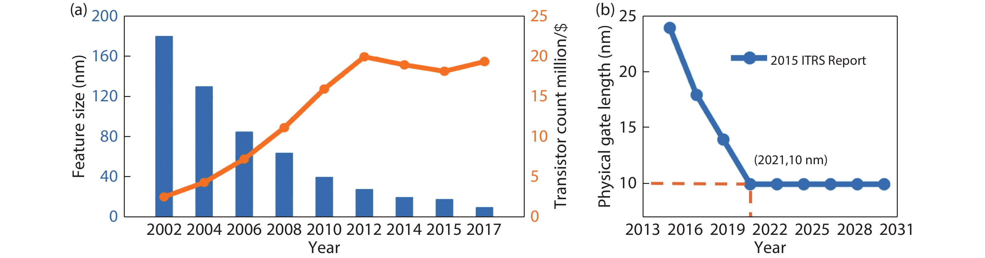
    Fig. 1. (Color online) (a) Number and size of transistors bought per dollar. Source: The end of Moore’s law. The Economist, April, 2015. (b) The ITRS most recent report predicts transistor scaling will end in 2021. Source: International Semiconductor Technology Roadmap (ITRS).
    (Color online) (a) The development trend of the semiconductor industry in the More-than-Moore Era. Source: International Semiconductor Technology Roadmap (ITRS). (b) Silicon photonics 2015–2024 market forecast. Source: Silicon Photonics Report Yole Développement.
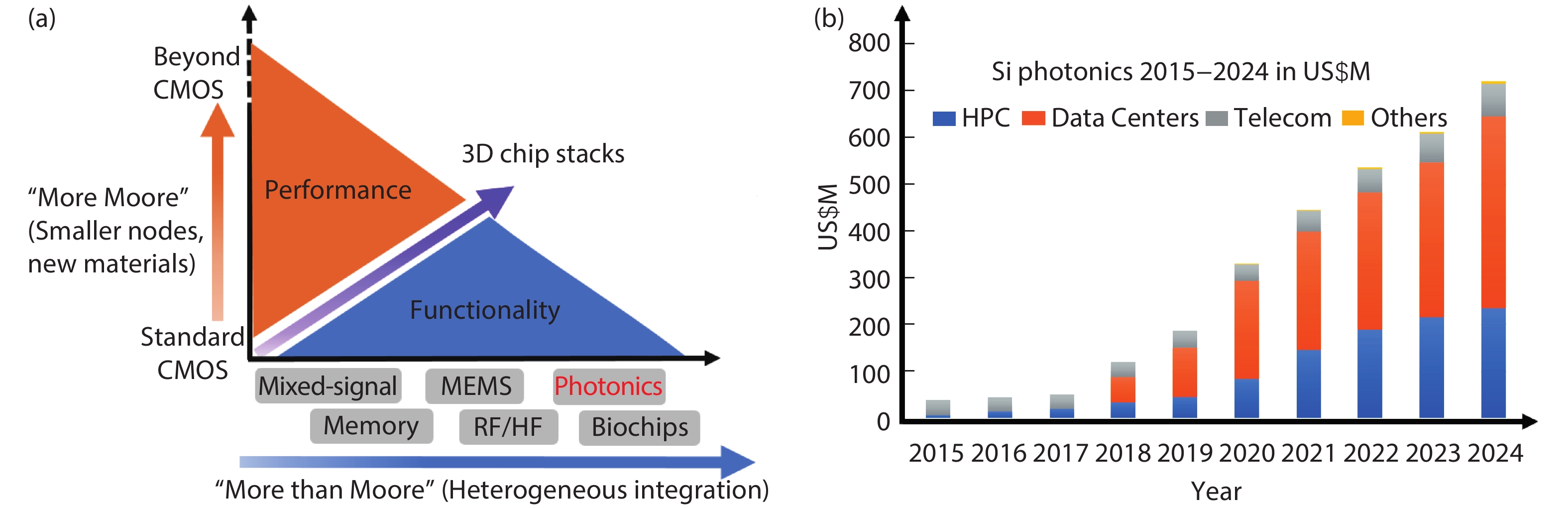
    Fig. 2. (Color online) (a) The development trend of the semiconductor industry in the More-than-Moore Era. Source: International Semiconductor Technology Roadmap (ITRS). (b) Silicon photonics 2015–2024 market forecast. Source: Silicon Photonics Report Yole Développement.
    (Color online) A summary of PCNC lasers (2010–2018). Insets show the device structures, materials, and threshold power, respectively.
    Fig. 3. (Color online) A summary of PCNC lasers (2010–2018). Insets show the device structures, materials, and threshold power, respectively.
    (Color online) (a) Schematic and (b) SEM of the proposed hybrid III−V/Si nanolaser attached to a conventional silicon-on-insulator (SOI) waveguide. (c) Measured output power near the end of the SOI waveguide (black) and near the InGaAsP nanobeam (red) against incident peak pump power. The inset shows a lasing emission spectrum near 1550 nm.
    Fig. 4. (Color online) (a) Schematic and (b) SEM of the proposed hybrid III−V/Si nanolaser attached to a conventional silicon-on-insulator (SOI) waveguide. (c) Measured output power near the end of the SOI waveguide (black) and near the InGaAsP nanobeam (red) against incident peak pump power. The inset shows a lasing emission spectrum near 1550 nm.
    (Color online) (a) Schematic of the proposed room temperature, suspended silicon nanobeam laser with a monolayer MoTe2 on top. The corresponding lasing spectra of the nanobeam laser under different pump power levels (b) using a grating resolution: 150 g/mm (0.41 nm), and (c) using a grating resolution: 600 g/mm (0.09 nm).
    Fig. 5. (Color online) (a) Schematic of the proposed room temperature, suspended silicon nanobeam laser with a monolayer MoTe2 on top. The corresponding lasing spectra of the nanobeam laser under different pump power levels (b) using a grating resolution: 150 g/mm (0.41 nm), and (c) using a grating resolution: 600 g/mm (0.09 nm).
    (Color online) (a) Schematic of the proposed TO tunable nanobeam filter. (b) SEM image of the fabricated PCNC filter. (c) Measured wavelength shifts against heating powers.
    Fig. 6. (Color online) (a) Schematic of the proposed TO tunable nanobeam filter. (b) SEM image of the fabricated PCNC filter. (c) Measured wavelength shifts against heating powers.
    (Color online) (a) SEM image of the proposed parallel quadrabeam PCNCs. (b) Real-time monitoring of streptavidin/biotin binding. Inset: resonance shift as a function of streptavidin concentration in PBS. (c) Resonance shifts as a function of the refractive indices with different concentrations ethanol/water solutions. (d) SEM of nanoscale sensor array. (e) Red shift of the targeted resonator occurs because of the higher refractive index of the CaCl2 solution. (f) Experimental data showing the redshifts for various refractive index solutions.
    Fig. 7. (Color online) (a) SEM image of the proposed parallel quadrabeam PCNCs. (b) Real-time monitoring of streptavidin/biotin binding. Inset: resonance shift as a function of streptavidin concentration in PBS. (c) Resonance shifts as a function of the refractive indices with different concentrations ethanol/water solutions. (d) SEM of nanoscale sensor array. (e) Red shift of the targeted resonator occurs because of the higher refractive index of the CaCl2 solution. (f) Experimental data showing the redshifts for various refractive index solutions.
    StructureMaterialDevice footprint (μm2) Modulation voltage (V)Modulation speed (GHz)Extinction ratio (dB)Energy consumption (J/bit)Year
    Si-polymer7.70.286132011[45]
    Si200.110–5100.52013[59]
    Si40.622061.4 × 10–172014[47]
    Si711.334.2 × 10–142014[48]
    Si-graphene20−6.413312.56 × 10–132015[53]
    Si-polymer3.6122410.97.5 × 10–162018[46]
    Si- ITO1.8920.1119.893.4845.9 × 10–192019[60]
    Table 1. Comparison with PCNC-based modulators.
    PrincipleStructureMaterialDevice footprint (μm2) Switching powerExtinction ratio (dB)Insertion loss (dB)Year
    Thermo-optic effectSi1 mW150.662016[68]
    Si45000.16 mW151.52017[69]
    Si141.52020[70]
    Electro-optic effectSi474 aJ/bit22015[71]
    Ge-on-Si3N48 pJ/bit60.972016[72]
    Si2002.6 fJ/bit14.21.22016[73]
    Kerr nonlinearityInP106 mW3.62014[74]
    Si311.6 pJ2442018[75]
    Si+polymer160.76 pJ2020[76]
    Table 2. Comparison with PCNC-based optical switches.
    StructureMaterialSensitivity (nm/RIU)QDetection limitYear
    Si83350002 pM2013[99]
    Si200200002012[100]
    Si269270002012[101]
    Polymer3863600010 mg/dL2011[102]
    Si410~100002013[103]
    Si451701510 ag/mL2014[104]
    InGaAsP461~100002015[105]
    Porous Si102390001.6 pm/nM2019[106]
    Table 3. Comparison with PCNC-based optical sensors.
    Daquan Yang, Xiao Liu, Xiaogang Li, Bing Duan, Aiqiang Wang, Yunfeng Xiao. Photoic crystal nanobeam cavity devices for on-chip integrated silicon photonics[J]. Journal of Semiconductors, 2021, 42(2): 023103
    Download Citation